A REVIEW OF DEVELOPING LOW NOISE AMPLIFIER INTEGRATED
NOTCH FILTER FOR VARIOUS TYPE OF APPLICATION
Nasrullah Saifullah, Zahriladha Zakaria, Azahari Salleh, Siti Rosmaniza Ab Rashid and Muhamad Fadhli
Muhamad Fadzil
Microwave Research Group, Centre for Telecommunication Research and Innovation (CeTRI), Faculty of Electronics and Computer Engineering, Universiti Teknikal Malaysia Melaka (UTeM), Durian Tunggal, Melaka, Malaysia
E-Mail: [email protected]
ABSTRACT
Nowadays, a number of low noise amplifiers have been developed to cover a multifunction capability such as Ultra wideband system, noise rejection and image rejection WLAN standard, GSM and others. Low noise amplifier is the one of important part in receiver. However, the integration of notch filter will introduce the multifunction which amplify and attenuate at single device. The notch filter commonly used as band rejection to remove unwanted frequency band so it could prevent for interference with other application. This paper presents a compilation of important review about design of low noise amplifier integrated notch filter and a regular low noise amplifier in term of various type of method, circuit, topology, matching technique and materials to cover various types of applications. Parameter reviewed for each paper is based on gain, input return loss and noise figure. In this particular review, hopefully that a greater knowledge of low noise amplifier concept might be developed thereby can have a better future.
Keywords: low noise amplifier, UWB, notch filter.
INTRODUCTION
Wireless technologies is fast growing and lots of standard involve is introduced. Most of the wireless is used as communication started with Global System for Mobile Communications (GSM), Wireless Local Area Network (WLAN), Worldwide Interoperability for Microwave Access (WiMAX) and the latest is Long Term Evolution (LTE).
Currently, the emerging wireless technologies require multifunction capabilities which a device that capable of running two or more function in a single device. In term of receiver, the need of multifunction is to support a function of amplifying and attenuating the received signal in a single device. Amplifying function is referred to amplifier and attenuating is referred to filter. The research of combining the functions leads to development of low noise amplifier with integrated notch filter.
Figure-1. Conventional based receiver.
Figure-2. Receiver system with LNA integrated notch filter.
A conventional based receiver consists of band pass filter and low noise amplifier which connected using external wires as shown in Figure-1. The uses of passive filter generally suffer from higher insertion loss due to the substrate and metal losses. Usually, band filtering is done by passive filter components such as SAW filters placed between the antenna and the receiver [1]. This loss will directly influence the NF of the system. However, the use of low noise amplifier with integrated notch filter (Figure-2) capable on reducing the size of the interface of the receiver and reduce the overall cost on designing the receiver while the noise can be minimize by the use of active notch filters as to improve the Q - factor[2]. Moreover, it can be designed more flexible in terms of tenability TX frequency and demanded selectivity, respectively and depending on the chosen structure the filter can be switched off to save power.
to rise until now with different method and matching technique to cover lots of application. Low noise amplifier with notch filter for Ultra-wideband system is the most popular design [1], [2], [3], [7-10]. Most of the notch filter design is focused on band rejection of 5-6 GHz which used on 802.11b WLAN standard. The notch filter also used to design multiband low noise amplifier which support multifunction capabilities [4], [6]. However, the entire low noise amplifier integrated notch filter is currently designed on CMOS process only but not on microstrip technology. To design low noise amplifier with microstrip technology, a suitable transistor need to be identified for specific application and desired noise figure and gain of the low noise amplifier. Furthermore, the substrate of the low noise amplifier also needs to figure
out in order to achieve optimum performance. However, there are several design of standard low noise amplifier using microstrip technology is presented [35-43].
LITERATURE REVIEW
Development of low noise amplifier integrated notch filter
Development of low noise amplifier with integration of notch filter is presented in Table-1. The design entirely is based on CMOS process. Most of the design used as band rejection for UWB systems whiles other focus on creating multi-standard low noise amplifier.
Table-1. Low Noise Amplifier integrated Notch Filter.
No. Paper Year, Authors Frequency (GHz) Technology Circuit
topology NF (dB) S11 (dB) S21 (dB)
1
A 1.3 V, 65nm CMOS,
Coilless Combined Feedback LNA with Integrated Single Coil
Notch Filter
(2009) D.
Bormann 1.73 UMTS, WCDMA 65nm CMOS
inductor-less two-stage feedback LNA
4 <-10 21.8
2
A Multi-band CMOS Low Noise Amplifier for
Multi-standard Wireless Receivers (2007) C. W.Ang (0.945) (2.4) 0.18µm CMOS 3-stage wideband LNA and 2 notch filters (4.7) (4.43) (-7) (-15) (18) (25) 3
0.18µm CMOS Low-Noise Amplifier with two
2nd-order notch filters for Ultra-Wideband
Wireless Receiver
(2007) C. C. Huang
(3.1 -4.9) (6.2 – 10.2)
0.18µm CMOS
2-stages shunt-peaked with notch filter
(2.5 ~3.3) (2.8~4.6) (<-8.6) (<6.4) (12.2~13.1) (12.2~15.5) 4
Design of Low Power CMOS LNA with
Current-Reused and Notch Filter Topology for DS-UWB
Application
(2012) M. T. Hsu
(3.1 – 5) (6 – 10.6)
0.18µm CMOS 2-stages common source, Current reuse (5)
(6.3) <-10
(15) (11)
5
Design of a Low Noise Amplifier with Integrated
Notch Filter for Interference Rejection in
Ultra- Wideband Systems
(2011) N. Koirala
(3.1 – 5.5) (5.7 – 10.6)
0.18µm CMOS 2-stages cascode and cascade stage, interstage LC component
3.5 >7 >17
6
A 20 GHz 1.9 dB NF LNA with Distributed Notch
Filtering for VSAT Applications
(2014) C. Lu (25 – 35) 0.25µm SiGe:C BiCMOS
two-stage
single-ended 1.9 --- 27.4
7 An Ultra-Wideband LNA with Notch Filter (2007) R. M. Weng 3.3 - 11 0.18µm CMOS
Common gate low noise amplifier with
notch filter
5 <-10 11.5
8
Analysis and Design of an Integrated Notch Filter for
the Rejection of Interference in UWB
Systems
(2009) A.
Vallese 1 - 9
0.13µm CMOS
4th order notch
filter cascode stage with an inductive
source degeneration
9
Design of Dual-Wideband Low Noise Amplifier base
on Common Gate Topology
(2013) M. T.
Hsu 3.1 – 10.6 0.18µm CMOS
common gate input stage and a cascade stage
with current-reused
4.8 <-10 18.7
10 Ultra-Wideband Front-End WithTunable Notch Filter (2006) K. A. Townsend 3.5 – 7.0 0.18µm CMOS 2
nd order with
bridged-T notch filter
4.1 < -10 12.1
11 WideBand Tunable LNA A 6 - 10-GHz Ultra- (2005) Y. C. Chen 6 - 10 0.18µm CMOS
Cascade configuration with inductive
source degeneration
4.2 <-9 11.6
Several researches on low noise amplifier integrated notch filter have been investigated. Most of the design of the low noise amplifier uses 0.18 µm CMOS process. For author C. Cheng (2007) [3], the design of low noise amplifier consist of wideband input impedances matching network, two stage cascade amplifiers with shunt-peaked load and integration of two 2nd - order notch filters. The simulation is based on TSMC 0.18µm standard RF CMOS process. The uses of shunt-peaked amplifier is because it easy to reach wideband bandwidth and eliminates the Miller effect on input transistor to achieve high frequency performance. The frequency band is divided into upper band and lower band which is 3.1- 4.9 GHz to 6.2-10.2 GHz. The advantages of using notch filter are to create a rejection band between 5 - 6 GHz to prevent interference between other devices. However, the authors compared the low noise amplifier with other design and find out that the power consumption of the low noise amplifier is quite higher which is 21.9 mW.
M. T. Hsu (2012), managed to design a low power Low Noise Amplifier with second staged with integration of notch filter for DS-UWB application [4]. Authors implement the method of current reuse structure in order to reduce the power consumption and integration of active second order notch filter to produce band rejection in 5 - 6 GHz frequency band. Authors divided the design into four parts which is input impedance matching, Noise analysis, Gain Analysis and Notch Filter. The use of common gate matching network is to achieve low and stable 50 Ω input matching, flat gain with sufficient linearity and low power consumption. Authors introduced the noise analysis to analyze the noise characteristic of the CGLNA by adding noise source to the small-signal equivalent circuit. In Gain Analysis, authors introduced the use of two-stage cascade architecture which is to achieve enough power gain and bandwidth. The first stage is designed resonate at the lower band, and the second stage is to resonate at the higher band. To achieve a flatness power gain, author implemented the inter-stage matching network.
In N. Koirala (2011), the authors introduced a fully integrated 0.18 µm CMOS Low Noise Amplifier with Notch filter for interference rejection at 5 - 6 GHz in UWB systems [5]. The circuit topology implemented by
authors is by using two -stages cascade and cascade stage with inter-stage LC component while notch filter comprises a series LC resonance circuit which with a resistance cancelation approach yields excellent attenuating characteristics. The matching used is shunt resistive feedback in order to achieve good input matching and low noise figure. Author stated that in order to obtain the high value of Q factor, the value of R need to be cancelled. Author introduced the use of Q-enhanced technique to utilize the negative gm cells which produce the negative resistance. This would compensate the losses of the LC circuit and boost Q of the lossy circuit. Authors divided the LNA design into two major stages which is cascade and cascade stages. For input stage, the cascade amplifier with resistive shunt feedback is used because of high reverse isolation and frequency response. For the second stage, authors implemented a common source amplifier with shunt inductive peaking to achieve high gain at high frequency and resistive shunt feedback to extend the bandwidth. The maximum gain achieved from 3.1 - 10.6 GHz is 18dB with minimum Noise Figure of 3.5 dB. The input return loss S11, is >7 dB with attenuation at rejection section >25 dB. The only disadvantage of the design is the low noise amplifier consumed high power which is 60mW.
connected at the output. Differential common source provides open loop gain which used to achieve sufficient real part of input impedance. Authors stated that he notch filter operates by drawing all current from the cascode output stage at the system’s own transmit frequency while introducing high impedance at all other frequencies which consist of series resonator build up from capacitor and inductor. This notch filter topology is crucial because a simple notch filter consist low selectivity at frequency offset as demanded by UMTS application.
C. Lu, M. K. M. Kammerer, R. Mahmoudi, P. G. M. Baltus (2014), designed a 20 GHz low noise amplifier with notch filtering which filter the frequency band from 27.5 GHz to 31 GHz by using 0.25 µm SiGe: CBiCMOS technology [6]. Authors decided to implement the notch filter at different stages in order to have minor impact on the noise figure while gaining high rejection around 30 GHz. The authors use two-stage single ended filtering which consists of cascode stage. In order to improve the linearity, the cascode stage is implemented with common emitter output stage. The transistor sized is rescaled to have the optimal noise resistance and the use of degeneration inductor will increase the input resistance to 50 Ω. The author uses the series inductance at the input which turns to achieve a simultaneous noise and power matching. In addition, the method also simplifies the input matching. The filter is implemented by using parallel LC lumped filter in series at the input matching. The second filter is combined before the cascode transistor. Further notch filtering is done between the first and second stage by using shunt series LC and series parallel LC filter. The Figure-3a and Figure-3b show the comparison between schematic diagrams of LNA with notch filter and without any filter while Figures 3c and 3d shows the gain and noise figure comparison between each respective. The gain is attenuated at desired band by using notch filter filtering compared with without filtering that does not affect the gain.
Figure-3(a). LNA with notch filter.
Figure-3(b). LNA without and filter.
Figure-3(c). S21 parameter result.
Figure-3(d). Noise figure result.
cascaded with different resonance frequencies. The uses of stagger tuning technique is to exhibit a bandpass like frequency response having maximal flatness around the centre frequency while the uses of common gate because it gas inherent wideband operating performance, good input-output isolation and batter electrostatic discharge compared with common source. The spiral inductor is chosen by the authors because of its relatively high Q factor. In second part, authors use the small-signal equivalent circuit of notch filter. However, the minimum noise figure achieved by the low noise amplifier is considerable higher compared with other low noise amplifier. The S - Parameter simulation is shown in Figure-4(a) and Figure-4(b).
Figure-4(a). S11 and S22 simulation.
Figure-4(b). S21 simulation.
The notch filter can be designed to be tunable. This is shown by K. A. Townsend, L. Belostotski, J. W. Haslett and J. Nielsen which designed low noise amplifier with integrated tunable notch filter for UWB receivers [10]. The design consists of two - stages low noise amplifier. The first stages claims to achieved wideband input match while the second stage is uses to implement the bridged - T filter for interferer cancellation. The
fabrication process chosen by the author is 0.18 µm CMOS. Authors claimed that the notch filter capable to tune from 3.5 GHz to 7.0 GHz with more than 40 dB of rejection. The first stage of the front-end is designed using cascaded by relying on transistor gate-drain parasitic capacitance to produce multiple matching mechanisms. the devices is stacked to produce the same effect while reducing current draw while the inductor use to isolate input device from transistor pair. For the notch filter, the use of bridged-T as a band rejection structure and the cancellation of notch frequencies can by determine by the value of R. Discrete tuning is enabled using a binary-weighted capacitive array with switches realized using multi-fingered NMOS devices.
Development of low noise amplifier with CMOS technology
Development of low noise amplifier by using CMOS technology is reviewed below. Several type of topology is implemented on the design in order to achieve the requirement for each application.
A design of low noise amplifier is improved by using body biased technique which is presented by J. Asmussen (2010) [16]. The advantages of using body biased are to decrease the supply voltage yet maintaining the current requirement and hence lower the power consumption. Authors implemented two cascaded stages which operating at two nearby frequencies to achieve wideband effect. The use of input shunt feedback is to achieve better input matching yet increasing the bandwidth cover by the low noise amplifier. Authors mention that the first stage is designed with both inductive degeneration and input shunt feedback in order to achieve better input matching and low noise figure. The second stage claims to provide gain. However, the linearity achieve is quite lower compared with other design stated in the paper.
A design of UWB LNA based on simple resistive shunt feedback technique is presented by X. Guan (2011) [29]. The design is claimed to perform well over the entire UWB band which is from 3.1 - 10.6 GHz. The design of LNA consist of two stage where the first stage has two transistor connected in cascode with a resistive shunt feedback and contain loading element in formed by the resistor parallel with the inductor. The loading element is important because the input impedance also depends on it. The second stage implements a source follower which contributes to the output matching and provides enough current to drive a 50 Ω load. Authors stated that the simplicity if the design make possible low power consumption, low noise figure, high linearity.
Development of low noise amplifier using microstrip technology
Development of low noise amplifier by using microstrip technology is reviewed below. In order to design the low noise amplifier using microstrip technology, it is required to identify a suitable transistor for desired application. The methodology on designing low noise amplifier is different between CMOS technology and microstrip technology.
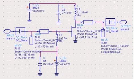
[image:6.595.311.547.105.243.2]C. L. Mayberry managed to design a low noise amplifier at 6 GHz using microstrip matching at the input and output using Duroid RO3006 substrate circuit board with pHEMTGaAs FET from Sirenza Microdevices [33]. The step on designing low noise amplifier by using microstrip technology is different compared with CMOS process technology. The author divided the step on designing the low noise amplifier into three parts which is stability consideration, initial analysis, minimum noise figure design and final design. In stability consideration part, the stability of the transistor is calculated in term of Rollet stability factor, K and delta. The author found that the stability of the transistor is 1.05 and delta is 0.25 and by referring to K > 1 and |Δ| <1, this make it unconditionally stable. Next, the initial analysis is conducted by analyze the performance limit of each parameter in term of calculation and graphically on Smith Chart. Author achieves to get 0.7 dB of minimum noise figure at 6 GHz and optimal reflection coefficient of 0.28∠179° from datasheet. The analysis is continued by calculating various types of gain such as maximum stable gain and maximum transducer gain. The value of VSWR is calculated and plotted into Smith Chart in order to identify a balanced VSWRIN and VSWROUT. Author continued to design the low noise amplifier into microstrip line by using Advanced Design System (ADS) software. Author decided to use single stub matching network which is the easiest matching network and easy to fabricated. The calculation involving the microstrip line is conducted using Smith Chart. Lastly, the optimization process is conducted to achieve optimum design of low noise amplifier by using ADS software. The final schematic of the optimized low noise amplifier is shown on Figure-5.
Figure-5. The final schematic of the optimized low noise amplifier.
The comparison between the ideal passive component and passive component implemented with microstrip is carried out by L. Daniel and M.Terrovitis (1999) in designing Broadband low noise amplifier [34]. Authors decided to implement two - stages low noise amplifier that cover through 3 GHz to 9 GHz by using GaAs MESFET transistor. Authors implemented common source topology by employing simplified small signal transistor model. A resonant circuit was employed by the authors in order to achieve a broadband matching of the generator impedance to the optimal source impedance which generate minimum noise figure. To reduce the minimum noise figure and increasing the VSWR, inductive degeneration technique is used which modify the input impedance. The two stage low noise amplifier is designed with both methods which is ideal passive component and passive component implemented with microstrip and the result is compared to identify which method is more optimum to implemented into the design. In order to convert the passive component into transmission line, the shunt capacitor is transformed in open stubs while the shunt inductor is transformed into shorted stub.
input matching and output matching but for multistage, it required to identify inter – stage matching network. Authors used LineCalc which is a tools that provided by ADS software to identify the physical dimension of the microstrip lines and stub which based on properties of substrate used and operating frequency. The disadvantages of the design are the parameter included in simulation is insufficient.
CONCLUSIONS
The integration of notch filter with low noise amplifier is rarely been research and develop. Various design is been reviewed and most of the design is based on CMOS process technology for various function and none of them is of microstrip technology. The used of CMOS process can be implemented on small device such as cell phone. However, the used of CMOS technology could introduce low power consumption but the process is expensive and hard to design. Thus, this could increase the cost of the product implemented by the chip. The use of microstrip technology could be implemented on large device such as radar, satellite and others. There are several low noise amplifier design is based on microstrip technology but none of them actually integrated with notch filter. An alternative technique on development of low noise amplifier with integrated notch filter with new topology by using microstrip technology can be proposed. The use of microstrip technology would reduce the cost of fabrication and easy to integrate into microwave circuit while applying the multifunction capability of amplifying and attenuating in a single device.
ACKNOWLEDGEMENT
The authors would like to thank UTeM for sponsoring this work under the research grant, UTeM, PJP/2013/FKEKK (41B)/20125.
REFERENCES
[1] D. Bormann, T. D. Werth, C. Schmits, S. Heinen. 2009. A 1.3V, 65nm CMOS, Coilless Combined Feedback LNA with Integrated Single Coil Notch Filter. 2009 IEEE Radio Frequency Integrated Circuits Symposium.
[2] C. W. Ang, Y. Zheng, C. H. Heng. 2007. A Multi-band CMOS Low Noise Amplifier for Multi-standard Wireless Receiver. Circuits and Systems, 2007. ISCAS 2007. IEEE International Symposium. pp. 2802-2805.
[3] C. C. Huang, Z. Y. Huang, Y. C. Wang, Y. T. Hung, M. P. Chen. 2007. 0.18um CMOS Low-Noise Amplifier with two 2nd-order notch filters for Ultra-Wideband Wireless Receiver. RFIT2007-IEEE
International Workshop on Radio-Frequency Integration Technology.
[4] M. T. Hsu, J. H. Du, W. C. Chiu. 2012. Design of Low Power CMOS LNA with Current-Reused and Notch Filter Topology for DS-UWB Application. Wireless Engineering and Technology. 3, 167-174.
[5] N. Koirala, R. K. Pokharel, A.I.A. Galal, H. Kanaya, K. Yoshida. 2011. Design of Low Noise Amplifier with Notch Filter for Interference Rejection in Ultra-Wideband System.
[6] C. Lu, M. Kammerer, R. Mahmoudi, P. G. M. Baltus. 2014. A 20GHz 1.9 dB NF LNA with Distributed Notch Filtering for VSAT Application. Microwave Symposium (IMS), 2014 IEEE MTT-S International. pp. 1-4.
[7] R. M. Weng, R. C. Kuo, P. C. Liun. 2007. An Ultra-Wideband LNA with Notch Filter, Radioelektronika. 2007. 17th International Conference. pp. 1-4.
[8] (A. Vallese, A. Bevilacqua, C. Sandner, M. Tiebout, A. Gerosa, A. Neviani. 2009. nalysis and Design of an Integrated Notch Filter for the Rejection of Interference in UWB System, Solid-State Circuits. IEEE Journal of. 44(2): 331-343.
[9] M. T. Hsu, P. Y. Lee, Y. Z. Huang. 2006. Design of Dual-Wideband Low Noise Amplifier base on Common Gate Topology, ASIC (ASICON). 2013 IEEE 10th International Conference. pp. 1-4.
[10]K. A. Townsend, L. Belostotski, J. W. Haslett, and J. Nielsen. 2006. Ultrawideband front-end with tunable notch filter. Circuits and Systems, 2006 IEEE North-East Workshop on. pp. 177-180.
[11]Y. C. Chen, C. N. Kuo. 2005. A 6 - 10 GHz Ultra-Wideband Tuneable LNA. Circuits and Systems, 2005. ISCAS 2005. IEEE International Symposium. pp. 5099-5102.
[12]A. Ismail, A. A. Abidi. 2004. A 3 - 10GHz Low Noise Amplifier with Wideband LC-Ladder Matching Network, Solid-State Circuits. IEEE Journal of. 39(12): 2269-2277.
[14]C. W. Kim, M. S. Kang, P. T. Anh, H. T. Kim, S. G. Lee. 2005. An Ultra-Wideband CMOS Low Noise Amplifier for 3 -5 GHz UWB System, Solid-State Circuits. IEEE Journal of. 40(2): 544-547.
[15]A. Bevilacqua, A. M. Niknejad. 2004. An Ultra wideband CMOS Low-Noise Amplifier for 3.1 - 10.6 GHz Wireless Receivers, 2004 Solid-State Circuits. IEEE Journal of. 39(12): 2259-2268.
[16]J. Asmussen, S. P. Sah, X. M. Yu, D. Heo. 2010. A Wideband Body Biased Low-Noise Amplifier. International Conference on Green Circuit and System, Shanghai. pp. 687-690, 21-23.
[17]R. Gharpurey. 2005. A Broadband Low-Noise Front-End Amplifier for Ultra Wideband in 0.13µm CMOS. Solid-State Circuits, IEEE Journal of. 40(9): 1983-1986.
[18]I. C. Chen, J. R. Yang. 2010. 3-10 GHz CMOS distributed amplifier low power and high gain low noise amplifier for UWB systems. TENCON.
[19]S. M. Wang, C. C. Chen, L. C. Yang. 2007. A Dual-Band Low Noise Amplifier in Enhancement-mode GaAspHEMT Technology. Asia-Pacific Microwave Conference. pp. 1-4.
[20]L. Yan, V. Krozer, S. Delcourt, V. Zhurbenko, T. K. Johansen, C. Jiang. 2009. GaAs Wideband Low Noise Amplifier Design for Breast Cancer Detection System. Microwave Conference, 2009. APMC 2009. Asia Pacific. pp. 357-360.
[21]G. Moschetti, N. Wadefalk, P.-Å. Nilsson, M. Abbasi, L. Desplanque, X. Wallart and J. Grahn. 2012. Cryogenic InAs/AlSb HEMT Wideband Low-Noise IF Amplifier for Ultra-Low-Power Application. IEEE Microwave and Wireless Component Letters. 22(3): 144-146.
[22]F. Ghadimipoor. H. G. Garakani. 2011. A Noise-Canceling CMOS Low-Noise Amplifier for WiMAX. 2011 International Conference on Electronic Devices, Systems and Applications (lCEDSA). pp. 165-169.
[23]T. K. K. Tsang, M. N. El-Gamal. 2002. Gain and Frequency Controllable Sub-1V 5.8 GHz CMOS LNA. Circuits and Systems, 2002. ISCAS 2002. IEEE International Symposium on. 4: 795-798.
[24]Y. H. Yu, Y. J. E. Chen, D. Heo. 2006. An Ultra-low Voltage UWB CMOS Low Noise Amplifier. Asia-Pacific Microwave Conference. pp. 313-316.
[25]C. S. Wang, C. K. Wang. 2006. A 90nm CMOS Low Noise Amplifier Using Noise Neutralizing for 3.1-10.6GHz UWB System. Solid-State Circuits Conference, 2006. ESSCIRC. pp. 251-254.
[26]Y. C. Chen, W. K. Yeh, R. L. Wang, H. D. Yen. 2007. 2-10 GHz UWB Low Noise Amplifier Using A Cascode Structure with Resistive Shunt Feedback. Asia-Pacific Microwave Conference. pp. 1-3.
[27]S. C. Chen, R. L. Wang, H. C. Kuo, M. L. Kung, C. S. Gao. 2006. The Design of Full-Band (3.1 - -10.6 GHz) CMOS UWB Low Noise Amplifier with Thermal Noise Canceling. Asia-Pacific Microwave Conference. pp. 409-412.
[28]C. Y. Wu, Y. K. Lo, M. C. Chen. 2009. A 3-10 GHz CMOS UWB Low-Noise Amplifier With ESD Protection Circuit”, Microwave and Wireless Components Letters, IEEE. 199(11): 737-739.
[29]X. Guan, C. Huynh, C. Nguyen. 2011. Design of a 0.18-µm CMOS Resistive Shunt Feedback Low-Noise Amplifier for 3.1 - -10.6 GHz UWB Receivers. Infrared, Millimeter and Terahertz Waves (IRMMW-THz), 2011 36th International Conference. pp. 1-2.
[30]N. Gautam, M. Kumar, A. Chaturvedi. 2014. A 3.1 - 10.6 GHz Two Stage Cascade Low-Noise Amplifier for UWB System. Communication Systems and Network Technologies (CSNT), 2014 Fourth International Conference. pp. 1070 - 1073.
[31]A. Djugova, J. Radić, M. Videnović-Mišič, L. Nagy, Lj. Živanov. 2014. Compact UWB Resistive Feedback Low Noise Amplifier Utilizing Current Bleeding Technique. Microelectronics Proceedings - MIEL 2014, 2014 29th International Conference. pp. 387-390.
[32]W. Wang, N. Peng. Y. Wang. Y. Xiong, B. Han, Q. N. Zhou, W. Ruan, F. Tan. 2010. Design of Low Noise Amplifier with Shunt Feedback for 3-5 GHz UWB Receiver. Communication Technology (ICCT), 2010 12th IEEE International Conference. pp. 269-271.
[34]L. Daniel, M. Terrovitis. 1999. A Broadband Low Noise Amplifier. Department of Electrical Engineering and Computer Sciences University of California.
[35]M. Challal, A. Azrar, D. V. Janvier. 2011. K-Band Two Stages Low Noise Amplifier Design in Microstrip Technology. Eighth International Multi-Conference on Systems, Signals and Devices (SSD’11).
[36]M.H CheHalim, M. Z. A. Abd Aziz, A. Rani Othman, S.A. Sahingan, M.F. Selamat, A.A. Abd Aziz. 2008. Low Noise Amplifier for Front End Transceiver at 5.8 GHz. Electronic Design, 2008. ICED 2008. International Conference. pp. 1-4.
[37]M. Challal, A. Azrar, H. Bentarzi, D. V. Janvier. 2008. Microstrip Design of Low Noise Amplifier for Application in NarrowBand and WideBand. Signals, Circuits and Systems, 2008. SCS 2008. 2nd International Conference. pp. 1-4.
[38]M. Challal, A. Azrar, H. Bentarzi, A. Recioui, M. Dehmas. 2008. On Low Noise Amplifier Design for Wireless Communication Systems. Information and Communication Technologies: From Theory to Applications, 2008. ICTTA 2008. 3rd International Conference. pp. 1-5.
[39]M. A. Bashir, M. M. Ahmed, U. Rafique, Q. D. Memon. 2013. Design of a Ku-Band High Gain Low Noise Amplifier. 2013 IEEE International RF and Microwave Conference (RFM2013). pp. 168-171.
[40]M.H CheHalim, A. Rani Othman, S.A Sahingan, M.F Selamat, A.A Abd Aziz. 2008. 5 - 6 GHz Front End Low Noise Amplifier, Telecommunication Technologies 2008 and 2008 2nd Malaysia Conference on Photonics. NCTT-MCP 2008. 6th National Conference. pp. 136-139.
[41]K. Pongot, A. R. Othman, Z. Zakaria, M. K. Suaidin, A. H. Hamidun. 2013. High Gain and Low Noise Single Stage Cascoded Lna Amplifier with Optimized Inductive Drain Feedback for Direct Conversion Wimax Rf Front End Receiver. Australian Journal of Basic and Applied Sciences.
[42]K. Pongot, A. R. Othman, Z. Zakaria, M. K. Suaidin, A. H. Hamidun. 2013. Double - Stage High Gain and Low Noise Cascoded LNA Amplifiers With Optimized Inductive Drain Feedback for Direct
Conversion WiMAX RF Front-end Receiver. Australian Journal of Basic and Applied Sciences.