A Novel Integration of Solar Fed Dynamic Voltage
Restorer for Compensating Sag and Swell Voltage in
Distribution System Using Enhanced Space Vector
Pulse Width Modulation (ESVPWM)
Viswaprakash Babu1,2,*, S. Sathik Basha3, Y. Mohamed Shuaib1, M. Manikandan2, S. Syed Enayathali4
1Department of EEE, B. S. Abdur Rahman Crescent Institute of Science and Technology, India 2Department of EEE, Jyothishmathi Institute of Technology & Science, India
3Department of Physics, B. S. Abdur Rahman Crescent Institute of Science and Technology, India 4Department of Civil, Anna University, India
Received October 24, 2019; Revised November 26, 2019; Accepted December 4, 2019
Copyright©2019 by authors, all rights reserved. Authors agree that this article remains permanently open access under the terms of the Creative Commons Attribution License 4.0 International License
Abstract This proposed work describes a novel
optimal use of the system to be used for Photovoltaic (PV) based on Dynamic Voltage Restorer (DVR) voltage restoration, voltage regulation functions, and an active filter is represented. The power transmitting in the distribution system needs to be high quality of power to drive a load with efficiency. The most of the loads are non-linear loads. It causes the Total Harmonics Distortion (THD) in the system. These THD produces the system oscillation, capacitor overloading, drops in efficiency, voltage fluctuation, which create the poor operating performances of the consumer utilities. Essentially, when the load voltage is greater or lesser (sag and swell) than the actual voltage, the control system will analyses the demanded load voltage and it will be compensate by the solar-based DVR, which will improvise the energy consumption of the system. Technically those sag and swell voltage will be minimized with the help of DVR, but it needs advance control technique which will provide the effectiveness of the system. In this work, the Enhanced Space Vector Pulse Width Modulation (ESVPWM) is performing a proper switching pulse to the DVR inverter, which helps to improve the energy stabilization in the distribution system. The proposed DVR has additional benefits the operating voltage will observe from the solar PV which had perturb and observe (P&O) based Maximum power point Tracking (MPPT) system and will efficiently provide the DC power. The execution of solar Fed DVR is simulated under dynamic conditions with the variousparameters like steady-state error, Efficiency, Total Harmonics Distortion (THD) in the load. All those conditions performed in MATLAB-SIMULINK 2017bsoftware.
Keywords Dynamic Voltage Restorer, Distributed
Energy Resources, Harmonic Compensation, Perturb and Observe (P&O) MPPT Algorithm, Enhanced Space Vector PWM (ESVPWM)1. Introduction
Figure 1. Functional block diagram for DVR system A DVR with a controller has commonly implemented
for analyzing and compensating the transmitted voltage. The sensed load voltage will be passed through the system analyzer and will compare the load voltage with reference voltage. If there is any error occurs on the system, the ESVPWM is employed to obtain reference gate signals for MOSFET conversion, so that the switching pulse is set to the range of a kHz frequency to produce a 50 Hz sine wave three-phase voltage at the load ends [21]. The inverter can be used to maintain a voltage of 1per unit (P.U) on different types of load nodes. The controller has only accelerating signal, it depends upon the input and load voltages. The controller output module is in the form of an angle which is the extra phase-lagging lead of the three-phase voltage has stabilized. There are two modes of operation is implemented in DVR, standby mode and booster injection. During Standby mode (VDVR = 0) the injection transformer voltage is lesser than the converter voltage. The semiconductors do not change in this way, because the semiconductors of the individual converter switches is induced to the short circuit path is establish to the transformer, resulting in lower conduction losses. In some cases, the DVR transformer in this mode exerts a less amount of voltage stabilization for the voltage reduction due to rejection losses. In regulating condition DVR voltage greater than zero, DVR is used to give a compensating injected power with the magnitude and phase required by the transformer to increase as a supply voltage is detected [24]. This promising solution to these problems is Dynamic Voltage restorer (DVR), a series of compensation devices used to protect or drain a critical
load from voltage drop. In this work, modeling of photovoltaic cells and inverter are carried out and combined to form a perfect model using MATLAB-Simulink. Modeling and analysis of DVR are properly designed and the proposals are validated using MATLAB simulation studies. The reaming part of this work is organized as
Chapter 2 discuss the Literature survey based on existing PWM methods
Chapter 3 discuss the proposed DVR function with enhanced PWM Space Vector PWM
Chapter 4 discuss the simulation results and performance analysis of proposed system
Chapter 5 discuss the conclusion of the proposed work
2. Literature Survey
Some of the recent research related to power quality analysis in the grid system with reactive power compensations are discussed in this section.
unbalances the supply voltage along with distortions - drains the employee's voltage. Three-phase MEPLL absorbs essential positive, negative, and zero-order components through distorted - unbalanced waves [3-4].
Improving power quality using a DVR and enhancing the performance of a three-phase low-voltage rider integrated LVRT with a combined distributed generation (DG) system. The combine system PV and wind Power generator (WPG), which is an essential benefit of the load to provide the continues power [5].Implementation the D-Q control system will advance to more utilizing and fast-response characteristic to the Superconducting Magnetic Energy Storage (SME) system is to regulate the transient output voltage waveforms suddenly after voltage disturbances [6].The control Switching Frequency Based Sliding Mode scheme of the Conversion of Wind Energy System (WES) is regulating for wind power using DVR, for improved efficiency [7-12]. The DVR will enhance the DFIG wind turbine generation using stator flux decay compensation. Both the design and hardware results has been best, mainly two methodologies can adequately rotor current and improve the exhibition of the framework during network deficiencies [14].
The design methodology of the suggested FCL-DVR is fully discussed based on power systems computer-aided design (PSCAD)-electromagnetic transients including dc (EMTDC) simulation results validation is also carried out. Modeling and test ratings to ensure new FCL-DVR feedback capability for voltage compensation and fault current operation [15-18]. The new technique of DVR three-phase system has been recommended three-phase converter with a DC connector is to compensate for sag and swelling and voltage fluctuations - unbalanced voltage condition. This DVR architecture contains of two rectifier and inverter components with a combined DC links. The simplified design with control structures will optimize the test result [19]. A control scheme is presented using a two-step technique: first, to compensate for the DVR voltage speaker voltage; Second, the serial voltage phase exerts a reactive force. The implementation of this control method and its detailed testing has showing the reliability of the new technique solution of a DVR laboratory [20].
A significant power problem imposes a sudden reduction in the voltage drop from half a minute to a period of up to one cycle. Voltage compensation of substantial loads due to dynamic voltage restorer has its inevitable share of peak power among optional equipment [21].DVR Voltage related power quality issues are identified as a cost-effective solution to protect complex loads. The reduction and capacity charge can be improved by the elimination of the extension needle transformer [22].The term power is utilized to gauge control quality for modern, household, and business loads. In the electrical business, control quality is principally a basic concern [23].Dynamic voltage restorer (DVR) with fuzzy controller is mounted. Simulated particle swarm optimization based (PSO)
technique and fuzzy system is employed to adjust the parameters like, steady-state error, THD [24].The dynamic voltage restorer circuit is provided the basis for the model voltage recognition in the topology and control scheme [25].The main objective is to increase the power line voltage difference (and to determine the product between the fluctuation of power) and to help the systems maintain the main side (load) voltage level which is based on the compensation methodology [26].
The strategy used to control DVR depends on the reference law standard of changing to a three-phase inverter with the assistance of a voltage controller for hysteresis to keep up the voltage profile sinusoidal in the straight load terminal against the voltage profile [27]. Many have suggested a smooth switching DVR voltage control principle using the AC - AC converter output of a three-phase between a transformer input and output. Furthermore, reducing the essential elements it shouldn’t controls the system but also facilitates design consistency. Altogether things considered, certain exploratory outcomes are displayed to check the plausibility of the future delicate move 3 phase five-arm DVR [28].The voltage drop or failure creates ineffective conflict on the customer side and application side. DVR is a semiconductor with a booster transformer which maintains the power quality in load side, that is, to decrease control quality issues in the power system arrangement [29].The power generation provides a predictive voltage control scheme for the effective control of the Transformerless DVR. Predictive voltage control scheme uses a unique model of voltage source inverter (VSI) circuit and interfaces filter for the generation of the switching process of inverter switches. Furthermore, this system does not require any linear controller or modulation technique [30].
3. Materials and Methods
Figure 2. Proposed System Block Diagram
3.1. DVR Series Connected Topology
DVR is a series-connected electronic device that provides voltage on the transmission line to control the load side power. This system is typically connected between the distribution systems mainly on critical load feeder. The working operation of the DVR is compensated the load side voltage without any power disruption. Also, the voltage compensation for the transmitting system sags and swells, which can reduce the voltage transients and enhance the current limitations in the distribution systems to increase the voltage resonances.
[image:4.595.111.483.464.700.2]Figure 3 illustrates the circuit diagram for the series-connected DVR system, which consists of source voltage, DC link, injection transformer, load, active filter, and inverter.
3.1.1. DVR Voltage Correction Methods
The DVR voltage correction methods are ability to compensate the voltage fluctuation in the distribution system with a limited power rating and various load requirements. Some loads are very sensitive in preventing the use of power angle, and others voltage distortions are clearly analyzed with the control system. Hence, prevention methods depend on load properties. There are three several methods of a DVR voltage regulators listed below.
1. Pre-Sag-DIP Compensation (PSC or PDC) 2. In-Phase Compensation (IPC)
3. In-Phase Advance Compensation(IPAC) 3.1.2. PRE-SAG-DIP Compensation (PSC or PDC)
[image:5.595.323.513.199.363.2]In this method the series injected real power cannot be controlled and it is calculated by external fault condition are previously determined and compensated by using Pre-Sag-Dip Compensation.
[image:5.595.64.286.376.519.2]Figure 4. PDC based vector diagram
Figure 4, shows the reactive power of DVR equations are represented below,
S = 3 IV (1)
=𝐼�(𝑉𝐼2+𝑉𝑠2−2𝑉𝐼𝑉𝑠 cos(𝜃1− 𝜃𝑠) (2)
The real power of DVR is,
P = 3Il (Vl cosθl−Vs cosθs) (3) The phase of DVR voltage is,
𝑉=�(𝑉𝑙2+𝑉𝑠2−2𝑉𝑙𝑉𝑠 cos (𝜃1− 𝜃𝑠) (4)
𝜃= tan−1�𝑉𝑙 cos 𝜃𝑙𝑉𝑙𝑠𝑖𝑛𝜃𝑙−𝑉𝑠−𝑉𝑠sin 𝜃cos 𝜃𝑠𝑠� (5) Where,
P is an active power
𝑉𝑠is source voltage
I is current
S is apparent power
𝑉𝑙 is load voltage
In this mode, the DVR regularly examines at the supply voltage. In the DVR system, energy is lost between the sag and swell voltages. In the case of compensation, both the magnitude and the phase angle of the load voltage is compensated by DVR. Figure 5 shows the pre-sag conditions of the vector representation. In this mode, the boosted voltage couldn’t be controlled when the load voltage is reset. Determine the type of fault conditions and power applied to the load transfer line.
Figure 5. Phasors diagram of the PSC method
The voltage 𝑉𝑖𝑛𝑗 and phase angle 𝜃𝑖𝑛𝑗 to be injected
can be estimated as per equation.
𝑉𝑖𝑛𝑗=�𝑉𝑠𝑎𝑔2 +𝑉𝑝𝑟𝑒𝑠𝑎𝑔2 + 2𝑉𝑠𝑎𝑔+𝑉𝑝𝑟𝑒𝑠𝑎𝑔𝑐𝑜𝑠𝜃𝑠𝑎𝑔 (6)
θinj= tan−1Vpresagcosθpresag−VsagcosθsagVpresagsinθpresag (7)
Where,
𝑉𝑖𝑛𝑗 is injected voltage
𝜃𝑖𝑛𝑗 is phase angle
𝑉𝑠𝑎𝑔 is sag voltage
𝑉𝑝𝑟𝑒𝑠𝑎𝑔 is pre-sag voltage
3.1.3. In-Phase Compensation (IPC)
This is the most reliable and utilized system DVR method to compensate the load side voltage fluctuations the phasor diagram of IPC technique is shown in figure 6. In other words, this system demands the voltage to diminish the high level of real power, i.e., the energy storage device.
The phasors diagram of reactive power in DVR is shown in figure 6 and the mathematical formula of reactive power is represented as,
𝑆= 3 𝐼𝑙𝑉= 3 𝐼𝑙(𝑉𝑙− 𝑉𝑠) (8)
The real power of DVR is,
P = 3IlV cosθ s = 3 Il (𝑉𝑙− 𝑉𝑠) cosθs (9)
Scale and the DVR voltage angle,
𝜃𝑥𝐷𝑉𝑅=𝜃𝑠 (11)
Figure 6. Phasors diagram of the IPC method 3.1.4. In-Phase Advance Compensation (IPAC)
The combined operation of the both pre-sag and in-phase compensation is created to form an IPAC method. The pashor diagram of IPAC will be shown in figure 7, during this mode the active power is injected to the continuous loads. In different control strategies have limited timing and efficiency for regulating the load voltage which also needs an active power injection during compensation.
Phase advance methods prove useful in comparison to other methods because it only involves inject the reactive power compensation instead of active power. The dynamic force load is zero by injecting the compensated voltage right-angled to the current. The phase-in advance is much more detailed than the injected voltage or phase system. During high load condition the voltage phase shift will causes variance problem like, false zero interrupts and load power oscillation. Therefore, the phase advance
[image:6.595.61.296.81.225.2]compensation tolerance must be adjusted for the phase angle or when the position angle moves from the wrong angle to the forward angle.
Figure 7. Phasors diagram of the IPAC method 3.1.5. Injection - Booster Transformer
The injection-booster transformer is specially designed to control the noise and voltage fluctuations in the transmission line. Mainly it booster transformer contains two side winding primary and secondary it will connected to the HV line for injection of reactive power when unbalanced load voltage the primary side receives the voltage from the solar-based inverter system for backup power processing. Additionally injection-booster transformer will isolate the load from the system using inverter switch .The single-phase circuit diagram of booster transformer will be represented in figure 8.
Figure 8. Booster transformer
Vs
Bypass Switch
Injection Transformer
Filter
DC Power
Source
1
5
4
8
Load
[image:6.595.311.531.121.261.2] [image:6.595.110.475.469.682.2]3.2. PV-DVR System
The photovoltaic (PV) array is a combination PV cell that transforms solar energy into electrical energy. In this proposed model DVR based PV is connected DC to DC converter for providing in the stability DC voltage to the voltage source converter, the circuit diagram of the PV-DVR system is as represented in figure 9. It has been introduced between the photovoltaic and battery bank of the DC connection.
The rapid changing in climate conditions to produced
solar energy is unstable it requires DC-DC converter to provide constant voltage to the DVR inverter. It is working with the radiation intensity of the solar radiation, as well as the cell transition and temperature. Basic equations for batteries voltage, including PV array temperature change and voltage radiation intensity property, are being developed. One purpose of the photocurrent is that the voltage of the battery output voltage is often defined by the load current related to the amount of solar radiation. The circuit diagram of the solar cell is shown in figure 10.
Figure 9. Solar-based DVR system
[image:7.595.78.511.234.629.2]Vpv=qln(nKTIDC Ipv+1)
(12) Ipv= Isc−Ipvo (13)
Where,
𝑉𝑝𝑣 is photovoltaic voltage
𝐼𝑝𝑣 is photovoltaic current
K is Boltzmann constant T is cell reference temperature
𝐼𝑠𝑐 is short circuit current
𝐼𝑝𝑣𝑜is diode saturation current
3.2.1. Perturb and Observe (P&O) Based MPPT System MPPT is an important measurement of solar power tracking. The Perturb and observe (P&O) MPPT algorithm
apply a small increase or decrease of perturbing voltage dynamic voltage to the operating voltage of the PV unit. The PWM generator is a control signal (Vref) used to generate solar output voltage (VPV) and solar output current (IPV). The flow chart of P&O MPPT method exhibited in figure 11.
[image:8.595.80.518.285.716.2]The P&O MPPT operation mode is illustrated in the image above. The actual position (L) and V I parameters are measured by the value of the previous position (L-1). The real value is obtained from the specification of its previous condition is estimated from the product of V, and the first increase or reference voltage drop. The P&O MPPT will compare the Vref and generated voltage and produce the rated pulse width modulation (PWM) for the voltage stabilization.
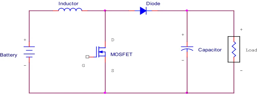
Figure 12. Circuit diagram for DC-DC Converter 3.2.2. DC to DC Converter
The converter circuit configurations, as shown in figure 12, which are used to regulate PV generated voltage and provide constant voltage to the circuit system. The DC to DC converter is used to improve the DC voltage when the input volt is lower than the output volt, and the boost converter is used to improve the voltage.
The general outline conditions of the converter are given below
𝑉𝐿= (14) Where,
𝑉𝑙= O−P voltage
𝑉𝑠= I-P Voltage
σ= clock pulse
Inductance required for the activity in terms of continuous conduction mode (CCM's) is Lmin,
𝐿𝑚𝑖𝑛= (( 1− 𝜎)2)𝜎𝑅𝑙)2𝑓𝑠 (15)
The capacitor voltage Vr is expressed at Cmin,
𝐶𝑚𝑖𝑛𝜎 − 𝑅𝑙𝑓𝑠𝑉𝑟 (16)
The load current 𝐼𝑜 as expressed as,
Io= (1− σ)Is (17)
Where I is the source current with the change in the current ∇I in light of the evaluation of inductance is given as,
∇𝐼=𝑉𝑠(𝑉𝐿−𝑉𝑠)
𝑓𝑠𝐿𝑉𝑙 (18)
Where, 𝑉𝑠= source voltage
𝑉𝑙= Load voltage
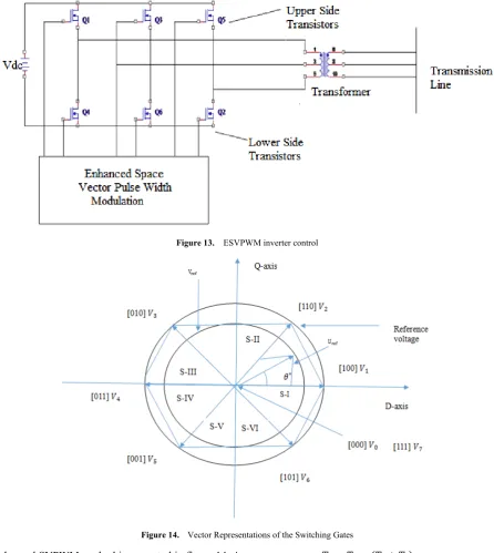
3.3. ESVPWM Control Strategy
The Enhance SVPWM technique is the efficient, computationally intensive Pulse width modulation method techniques and it had a potential regulated frequency to the converter depend upon the application needs. The typical 3 phase voltage source circuit design for PWM inverter is presented in figure 13. R, R′, Y, Y′, B and B' are the six switches that give the output from Q1 to Q6. When an upper side transistor is turned on, that is, R, Y or B 1, according to the lower side transistor is switched off, that is, relative ‘a’, ‘b’ or ‘c’. Therefore, transistors ‘Q1’, ‘Q3’, and ‘Q5’ are outputs of on and off positions can be used to determine the voltage.
Figure 13. ESVPWM inverter control
Figure 14. Vector Representations of the Switching Gates Enhanced SVPWM method is presented in figure 14. A
simple method of the Vref voltage vector is using eight changes to regulate the average inverter circuit output over a short period of time. In the same period, Vref should be T. 3.3.1. Determination of Time Durations 𝑻𝑻𝟏𝟏𝑻𝑻𝟐𝟐𝑻𝑻𝟎𝟎
From figure 11, can calculate the switching period,
𝑇1=𝑉𝑑𝑐√3𝑇𝑍�𝑉𝑟𝑒𝑓� �sin𝑛𝜋3 cos𝜃 −cos𝑛𝜋3 sin𝜃� (19)
𝑇2=𝑉𝑑𝑐√3𝑇𝑍�𝑉𝑟𝑒𝑓� �sin𝜃cos(𝑛−13)𝜋−cos(𝑛−13)𝜋sin𝜃�(20)
𝑇0=𝑇𝑍−(𝑇1+𝑇2) (21)
𝑇𝑍=𝐹1𝑧 (22)
Where n=1 within 6, is the vector region
𝑇𝑍= samping time
𝐹𝑧= Switching frequency
Table.1. ESVPWM Switching Table
Vector Q1 Q3 Q5 Q4 Q6 Q2 VAB VBC VCA
𝑉0={000} OFF OFF OFF ON ON ON 0 0 0
𝑉1={100} ON OFF OFF OFF ON ON +VDC 0 -VDC
𝑉2={110} ON ON OFF OFF OFF ON 0 +VDC -VDC
𝑉3={010} OFF ON OFF ON OFF ON -VDC +VDC 0
𝑉4={011} OFF ON ON ON ON OFF -VDC 0 +VDC
𝑉5={001} OFF OFF ON ON ON OFF 0 -VDC +VDC
𝑉6={101} ON OFF ON OFF ON OFF +VDC -VDC 0
𝑉7={111} ON ON ON OFF OFF OFF 0 0 0
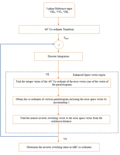
3.3.2. ESVPWM Algorithm Steps
Step 1: During the undesired condition to Change the switching time of the device, switch-mode type, and creates the real output of the control system produce different voltage vector.
Step 2: Method for converting a three-phase bridge arm of the eight switching state combinations can be created.
𝑉0− 𝑉7 Vectors
Step 3: In the sample time cycle, always beginning with the zero vector and ending with the zero vector, the plane is subdivided into six segments, two adjacent voltage vector switch and two zero vectors for a set of rotating space vector equivalent𝑢𝑟𝑒𝑓, followed by a regular polygon
approximation.
Step 4: The component 𝑠𝑒𝑡𝑈𝛼and 𝑈𝛽are 𝑈𝑐 intended
to define the three reference vector to determine the number of fields, define three reference vectors:
𝑢𝑟𝑒𝑓1=𝑢𝛽 (23)
𝑢𝑟𝑒𝑓2=𝑢𝛼𝑠𝑖𝑛𝜋3− 𝑢𝛽𝑠𝑖𝑛𝜋6 (24)
𝑢𝑟𝑒𝑓3=𝑢𝛼𝑠𝑖𝑛𝜋3− 𝑢𝛽𝑠𝑖𝑛𝜋6 (25) Step 5: The space voltage vector evaluation number N can be stated as:
𝑁=𝑆𝑔𝑛�𝑢𝑟𝑒𝑓1�+ 2𝑆𝑔𝑛�𝑢𝑟𝑒𝑓2�+ 4𝑆𝑔𝑛(𝑢𝑟𝑒𝑓1) (26)
Where, 𝑆𝑔𝑛 is space voltage vector.
Step 6: In a switching cycle, define the three-phase relative switching times, 𝑇1,𝑇2, and 𝑇0 for the vector of
switching points, for the point cutoff of the power pipe.
Step 7: The assumption is that A, B, high-level corresponding PWM ranges , where the C line switch is at the top of the switch's operating position when the low-level low-arm switch is in relative motion and does not switch on dead time and minimum pulse width.
Step 8: A phase change of the state status of restoration for each switch is selected to not only change the zero vector using the average allocation scheme
Step 9: To obtain the amplitude of the switching control pulse, A, B, C are the constant frequency and peak of the triangular wave as the carrier signal relative to the three-phase switching time waveform comparison.
Step 10: When the VS=VPK, regulate the pulse. VS=source voltage
VPK=triangular wave voltage
Step 11: It can find the characteristic triangle where space vector 𝑢𝑟𝑒𝑓 locates inconveniently.
Step 12: The positioning of the new original center vector 𝑉𝑜 is another problem to be solved as the level of
PWM increases, even with the difficulty of overlapping area handling for adjacent hexagons.
Step 13: The reference vector 𝑉𝑟𝑒𝑓curve is coordinated
by using at least three different switching positions of Ts during each transition period.
𝑠𝑤𝑖𝑡𝑐ℎ𝑖𝑛𝑔𝑝𝑒𝑟𝑖𝑜𝑑 (𝑇𝑠) =𝑠𝑤𝑖𝑡𝑐ℎ𝑖𝑛𝑔𝑓𝑟𝑒𝑞𝑢𝑒𝑛𝑐𝑦1 (𝑓 𝑠) Step 14: Each circle along the same output line switching states can generate unwanted voltages, indicate switching states.
Figure 15. Flow chart for the proposed ESVPWM method
Figure 15 represents the proposed Enhanced Space Vector PWM (ESVPWM) based DVR inverter, and its switching techniques are clearly explained.
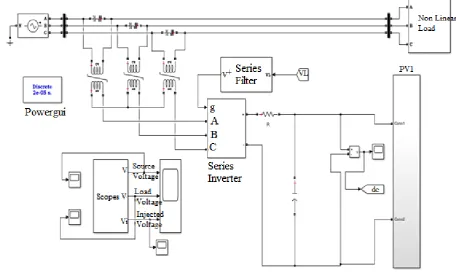
4. Results and Discussion
The Enhanced Space Vector PWM (ESVPWM) based DVR is implemented in MATLAB Simulink software system, and this design shown in figure 16, an Enhanced Space Vector PWM (ESVPWM) technique is provides an power quality in distribution system which performance are evaluated in the running condition.
which is present is low. The variation of proposed model with its output parameters like source voltage, load voltage and injection transformer voltage is view on the scope of the system.
Figure 17. Solar Power generation voltage
Figure 18. Simulated waveforms of Source Voltage for the proposed DVR model
Figure 19. DVR Injected Voltage
Figure 20. Simulated waveforms of Three Phase balanced Source Voltage for the proposed DVR model.
[image:17.808.66.754.83.343.2]Figure 21. THD Analysis of the proposed control system with a DVR
Figure 22. THD Analysis of the proposed control system without a DVR
Table 2. Performance analysis for DVR Features of the proposed and existing system
Parameters PI ESVPWM
Steady-state error (%) 1.8 0.9
Without DVR THD (%) 18 14
With DVR THD (%) 9.1 2.01
Efficiency (%) 88 91
Table 2 shows the comparison table for the (DVR), which are analyzed for the operating features of the existing system and proposed a system.
Steady-State Error:
Stability control is an essential characteristic of the system; Feedback control systems are used to compensate for disruption or unwanted inputs that enter an order.
ec(t) = cr(t)−c(t) (27)
Where
𝑒𝑐(𝑡) is a system error
𝑐𝑟(𝑡) is requested output
𝑐(𝑡) is practical output
Total Harmonics Distortion (THD)
The THD of any system can be calculated by the Equation (28) 2 1 .... 3 , 2 2
V
V
THD
∑
n n∞ =
=
(28)Where V1 and Vnare the amplitude of the essential
segment and harmonic requests of a waveform, separately. Considering every single harmonic application, which is required for an exact count of THD, is relatively unthinkable for those waveforms. Rather than Equation (28), another type of the THD recipe, which deals with the dominant estimation of the waveform, can consider every harmonic request in Equation (29).
1
2
2
, 1−
=
V
V
rms rmsTHD
(29)Where
V1, rms = Effective value of the fundamental component.
Vrms = Effective value of the whole waveform.
[image:20.595.69.523.414.630.2]Figure 23 is the comparative analysis of the DVR control which evaluates with various parameters like steady-state error, efficiency and with and without THD results are evaluated with the existing system the proposed Enhanced Space Vector PWM (ESVPWM) produce effective results.
Figure 24. THD Analysis
Figure 24 shows the Total Harmonics Distortion for the proposed model with DVR system is produces the better result of 2.01%.
5. Conclusions
This work provides a necessary analysis of the DVR that can reduce the voltage sag and swell disturbances in the load side distribution system. The proposed Solar based DVR model will be designed in the MATLAB Simulink software 2017b and its performance are evaluated with various parameters like steady-state, efficiency and Total Harmonics distortion (THD) will be examined with dynamic running condition. Additionally the proposed Enhanced Space Vector PWM (ESVPWM) algorithm used proper switching pulses under required condition to improve power quality in distribution systems in officially accepted procedures as various power lines disturbances such as voltage restoration, voltage deviation and THD of the system also compensated. Under dynamic time and load varying conditions the proposed ESVPWM that’s only produced better THD Result of 2.01%. Finally, the overall performance of the proposed solar-based DVR will improve the power quality of the distribution system in every arrangements of the proposed model and also increase the system efficiency 91% with low design cost.
REFERENCE
Shakir, Sharma, & Manish, (2019), ‘IRPT Based DVR [1]
Application for Voltage Enhancement’ in International Confer on Signal Processing and the Integrated Networks System, Confer Location: India.
Abhilash Krishna, A. & Karthikeyan, D.G, (2019), ‘Dual [2]
Role CDSC based Dual Vector Control for Efficient Operation DVR system with Harmonic Mitigation’ in IEEE Trans on Industrial Electronics, Vol. 66, Issue. 1, Pages no:
4-13.
Peng Yao & Zhikang Shuai, (2015) ‘Design and [3]
Considerations of a Fault Current with Preventive analysis of DVR’ IEEE Trans on Smart Grid system, Vol. 6, .Issue. 1, Pages no. 14-25.
Yao Sun & Min Zhou1, (2018) ‘Transformer-less DVR [4]
based on a 3-leg ac to ac converter’ in IET Power Electronics, Vol. 11, Issue. 13, Page. 2045-2052.
Aurelio Garcıa-Cerrada, Javier Roldan-Perez, (2019), [5]
‘Delayed Signal Cancellation based Sag detection for a DVR in distorted grids’ in IEEE Trans on sustainable energy system, vol .10, no. 4, pp. 2015-2027
Linfang Yan & Xia Chen, (2018), ‘A Novel DVR ESS with [6]
embedded Windpower Conversion System’ in IEEE Trans on Sustainable Energy, Vol. 9, Issue. 3, Pages. 1265-1274. Linfang Yan, & Xia Chen, (2018), ‘Perturbation and [7]
compensation based non-linear adaptive control system for ESS DVR for the LVRT capability improvement of wind system’ in IET Renewable Power Generation, Vol. 12, Issue. 13, Pages. 1500-1507.
Ebrahim Babaei, Farzad & Mohammadzadeh Shahir, (2017), [8]
‘Compensation of Voltage Sags and Swells using Photovoltaic system Based DVR’ in International Conference on Electrical Engineering, Computer, Electronics, Telecommunications and Information Technology, Confer Location: Phuket, Thailand.
Dongqiang JIA, & Zhaoquan WANG, (2017), ‘The [9]
Interaction Analysis of Comprehensive Compensation’ in IEEE Trans Electrification Confer and Expo, Asia-Pacific, Conference Location: Harbin, China.
Fujin Deng, & Rongwu Zhu, (2016), ‘Enhanced control of [10]
DFIG system wind turbine based on stator flux decay compensation’ in IEEE Trans on Energy Conversion, Vol. 31, issue. 4, Pages. 1366-1376.
Zhikang Shuai, &Peng Yao, (2015), ‘Design Considerations [11]
of a Fault Current Limiting DVR’ in IEEE Trans on Smart Grid, Vol. 6, Issue. 1, Pages. 14-25.
Mariesa L, Deepak Somayajula, & Crow, (2015), ‘An [12]
Sustainable Energy, Vol. 6, Issue. 2, Pages. 616-624. Ahmed Moawwad, & Surour Alaraif, (2013), ‘Voltage [13]
Booster Schemes for Fault Ride-Through improvement of Variable Speed Wind Turbines’ in IEEE Trans on Sustainable Energy, Vol. 4, Issue. 4, Pages. 1071-1081. Abir Chatterjee & Ali Keyhani, (2012), ‘An Automatic [14]
Generation of Control Arrangement for Smart Grids’ in IEEE Trans on Smart Grid, Vol. 3, Issue. 3, pages. 1310-1316.
Abdul Basith M & B, Sunitha K, (2017), ‘A Novel approach [15]
of DVR Integration with Ultra Capacitor for Proper Voltage Sag Compensation’ International Confer on Power, Control, Signals and Instrumentation Engg.
Ravi Kumar, & Ansal. K, (2016), ‘Transformer less DVR [16]
for Voltage Sag Mitigation’ in biennial international confer on power and energy systems, Towards Sustainable Energy. Arun Benhail, & Venkatesh Kumar, (2017), ‘Modeling and [17]
Simulation of a Single Phase Transformerless DVR for commercial Application’ International Confer on Innovations in Electrical, Electronics, Instrumentation and Media Technology ,pp. 364-366, Coimbatore, India Faranak Farhadi & Sajjad Solat, (2015) ‘Optimal DVR [18]
Controller for Voltage Sag Compensation’ in Iranian Confer on Electrical Engg, pp. 1705-1078, Tehran, Iran Shaogui Fan, KuoGai, Kaitao Bi, & and Li Sun, (2017), ‘A [19]
Method of Voltage Detection Specific to Single Phase DVR’ IEEE Transportation electrification confer and expo, pp. habrin, Chinna
Priya Gupta & Ankur Kumar Gupta, (2018), ‘A Novel [20]
Control Scheme for Single and Three phase Dynamic Voltage Restorer Using PSCAD and EMTDC’ in International Conference on Smart Electric Drives & Power System.
Ilamkar, Tejaswita L. & Vidyulata Joshi, (2018), ‘Voltage [21]
Sag Compensation Using synchronously reference frame theory-based DVR’IEEE International Confer on Current Trends toward Converging Technologies, Coimbatore. Maoh-Chin Jiang and Min-Lun Tsai, (2017), ‘A [22]
soft-switching Three-Phase Five-Arm Dynamic Voltage Restorer’ in IEEE peds, Honolulu, HI, USA
Mishra, Senior and Chandan Kumar, Mahesh K, (2015), [23]
‘Predictive Voltage Control of Transformer-less DVR, IEEE Trans on industrial electronics ,vol. 62, no. 5, pp. 2693-2697
Dr. M. Manikandan and Vishwaprakash Babu, 2017 Total [24]
Harmonic Distortion Reduction for Power Quality Improvement: A Review, International Journal of Science and Research (IJSR) ISSN (Online): 2319-7064 Index Copernicus Value (2015): 78.96 Impact Factor (2015): 6.391 pp. 1681-1684
Manikandan M, Mahabub Basha A 2016, Optimized Dual [25]
Fuzzy Flow Controller-Based Voltage Sag Compensation for SMES-based DVR in Power Quality Applications , Circuits and Systems, Scientific Research Publication, Acceptance, May 12, 2016. (A-I)
Manikandan, M & Mahabub Basha A 2016, ‘Voltage Sag [26]
Compensation Using DVR Based Superconducting
Magnetic Energy Storage Coil with PI Controller’, Asian Journal of Research in Social Science and Humanities, Accepted for publication. (Updated list-2016).
Manikandan M., Mahabub Basha A 2013, Power Quality [27]
Compensation Using SMES Coil With FLC, International Journal of Advances in Engineering & Technology, Vol. 6, Issue 4, pp. 1855-1868.
Ashwanth, S. Manikandan M, and Mahabub Basha A 2014, [28]
Superconducting Magnetic Energy Storage System based Improvement of Power Quality on Wind-PV Systems, International Journal of Emerging Technology and Advanced Engineering, Volume 4, Issue 4.(A-II)
Manikandan M, Mahabub basha A. and Arul R 2015, A [29]
Novel Reduced Switch Power Quality Improvement for Current Harmonic Compensation and Voltage Sag Mitigation Using Model Predictive Control, International Journal of Advanced Research in Electrical, Electronics and Instrumentation Engineering, Vol. 4, Issue 12.
Ashwanth. S and Manikandan. M 2014, Enhancement of [30]