ISSN :2394-2231 http://www.ijctjournal.org Page 72
ANALYSIS OF CMOS BASED FULL ADDERS FOR
MOBILE COMMUNICATIONS
V. Manojna
1, Mr. P. Koteswara Rao
2, Dr. Ch. Subrahmanyam
31
(Department of Electronics and Communication Engineering, GDMM College of Engineering and Technology, Nandigama.)
2
(Head of the Department, GDMM College of Engineering and Technology, Nandigama.)
3
(Department of Technical Education, Vijayawada.)
---
************************
---Abstract:
As technology scales into the nanometer regime leakage power and noise immunity are becoming important metric of comparable importance to active power, delay and area for the analysis and design of complex arithmetic and logic circuits. In this project, low leakage 1 -bit full adder cells are proposed for mobile applications.For the most recent CMOS feature sizes (e.g., 180nm), leakage power dissipation has become an overriding concern for VLSI circuit designers. The main goal is to reduce leakage power. Therefore a new transistor resizing approach is used for 1-bit Full Adder cells. The simulation results depicts that the proposed design also leads to efficient 1-bit full adder cells in terms of standby leakage power. In order to verify the leakage power, various designs of full adder circuits are simulated using DSCH, Micro wind and Virtuoso (Cadence).
Keywords —CMOS, 1-bit Full Adder, leakage power, noise immunity.
---
************************
---I. INTRODUCTION
In recent years, several variants of different logic styles have been proposed to implement 1-bit adder cells. These adder cells commonly aimed to reduce power consumption and increase speed. These studies have also investigated different approaches realizing adders using CMOS technology. For mobile applications, designers have to work within a very tight leakage power specification in order to meet product battery life and package cost objectives. The designer's concern for the level of leakage current is not related to ensuring correct circuit operation, but is related to minimize power dissipation.
An When an electronic device such as a mobile phone is in standby mode, certain portions of the circuitry within the electronic device, which are active when the phone is in talk mode, are shut down. These circuits, however, still have leakage currents running through them. The leakage current depletes the battery charge over the relatively long standby time, whereas the operating current during
talk time only depletes the battery charge over the relatively short talk time.
As a result, the leakage current has a disproportional effect on total battery life. This is why building low leakage adder cells for mobile applications are of great interest.
International Journal of Computer Techniques
mode while providing reduced leakage power consumption at a cost of slightly increased delay. Furthermore, the sleepy stack approach can be applicable to single- and dual-threshol
technologies.
A. Design considerations in Integrated Circuits
A circuit is specified to operate at a particular dissipation; area of implementation and reliability issues are subjects which designer must take into account. However, reducing
capacitance, which is another way to lower delay, reduces both power and delay. Generally, great power savings can be achieved if delay is not an issue, but optimizing power without delay consideration is insignificant delay, otherwise the entire system may not work.
B. Why low power?
With the continuous increase of the density and performance of integrated circuits due to the scaling down of the CMOS technology, reducing power dissipation becomes a serious problem that every circuit designer has to face.
Power dissipation limitations come in two ways. The first is related to cooling considerations when implementing high performance systems.
The second failure of high-power circuits relates to the increasing popularity of portable electronic devices. In today’s technology, the main contributer to static power consumption of a CMOS circuit is subthreshold leakage. The subthreshold leakage current can be expressed as follows:
Where K1 and n are experimental values, the width of the transistor, Vth is the threshold voltage and Vθ is the thermal voltage.
C. What is ground bounce noise?
As signal rise times continue to increase, a phenomenon called "ground bounce" begins to be an issue. It is a source of circuit noise and signal distortion that occurs inside an IC package. How much current flows depends on, among other things,
International Journal of Computer Techniques -– Volume 4 Issue 6, 2017
mode while providing reduced leakage power consumption at a cost of slightly increased delay. Furthermore, the sleepy stack approach can be threshold voltage
Design considerations in Integrated Circuits
A circuit is specified to operate at a particular dissipation; area of implementation and reliability issues are subjects which designer must take into interconnect capacitance, which is another way to lower delay, reduces both power and delay. Generally, great power savings can be achieved if delay is not an issue, but optimizing power without delay elay, otherwise the
With the continuous increase of the density and performance of integrated circuits due to the scaling down of the CMOS technology, reducing power dissipation becomes a serious problem that Power dissipation limitations come in two ways. The first is related to cooling considerations when implementing high performance systems.
power circuits relates to the increasing popularity of portable In today’s technology, the main contributer to static power consumption of a CMOS The subthreshold leakage current can be expressed as follows:
are experimental values, W is is the threshold
As signal rise times continue to increase, a phenomenon called "ground bounce" begins to be se and signal distortion that occurs inside an IC package. How much current flows depends on, among other things,
how many devices (loads) are connected to the output. The loads tend to be capacitive, so the initial current spike is not negligible. The out
(Vout) is measured between the output pin of the device and Ref B, which is at ground.
Fig1 A CMOS Inverter
II. TECHNIQUES FOR
DESIGN
D. Components of power consumption
Power consumption in a static CMOS circuit basically comprises three components: dynamic switching power, short circuit power static power. Compared to the other two components, short circuit power normally can be ignored in submicron technology.
Dynamic power is due to charging and discharging the loading capacitances. It can be expressed by the following equation
E. Leakage Power
The leakage current of a transistor is mainly the result of reverse-biased PN junction leakage sub- threshold leakage and gate leakage illustrated in Figure 2.
Fig2 Leakage currents in an inverter.
In submicron Technology, the reverse
2017
how many devices (loads) are connected to the output. The loads tend to be capacitive, so the initial current spike is not negligible. The output voltage (Vout) is measured between the output pin of the device and Ref B, which is at ground.
A CMOS Inverter
FOR LOW POWER
Components of power consumption
Power consumption in a static CMOS circuit basically comprises three components: short circuit power and . Compared to the other two components, short circuit power normally can be ignored in submicron technology.
ic power is due to charging and discharging the loading capacitances. It can be expressed by the following equation
The leakage current of a transistor is mainly junction leakage, ate leakage as
currents in an inverter.
reverse-biased PN junction leakage is much smaller than sub-threshold and gate leakage and hence can be ignored. The sub-threshold leakage
inversion current between source and drain of an MOS transistor when the gate voltage is less than the threshold voltage. It is given by:
Isub = µ 0 Co x (W/Leff) VT 2 e1.8 exp ((V
nVT) (1-exp (-Vds / VT))
Due to the exponential relation between Isub and Vth, an increase in Vth sharply reduces the sub-threshold current.
Gate leakage is the oxide tunneling
due to the low oxide thickness and the high electric field which increases the possibility that carriers tunnel through the gate oxide.
Where Vox is the potential drop across the thin oxide, Φox is the barrier height for the tunneling particle (electron or hole), and Tox
thickness. A and B are physical param by,
Where m is the effective mass of the tunnelling particle, q is the electronic charge, and
reduced Plank’s constant. The oxide thickness decreases with the technology scaling to avoid the short channel effects.
F. Techniques for Leakage Reduction
Leakage is becoming comparable to dynamic switching power with the continuous scaling down of CMOS technology. To reduce leakage power, many techniques have been proposed, including dual-Vth, multi-Vth, body bias, transistor
and optimal standby input vector selection
1) Dual-Vth Assignment
Dual-Vth assignment is an efficient technique for leakage reduction. In this method, each cell in the standard cell library has two versions, low Vth and high Vth. Gates with low biased PN junction leakage is much smaller than
threshold and gate leakage and hence can be threshold leakage is the weak inversion current between source and drain of an MOS transistor when the gate voltage is less than
exp ((Vgs-Vth) /
(2.2)
nential relation between sharply reduces the s the oxide tunnelings current due to the low oxide thickness and the high electric field which increases the possibility that carriers
is the potential drop across the thin is the barrier height for the tunneling is the oxide are physical parameters given
is the effective mass of the tunnelling is the electronic charge, and h is the reduced Plank’s constant. The oxide thickness Tox technology scaling to avoid the
Leakage is becoming comparable to dynamic switching power with the continuous scaling down of CMOS technology. To reduce leakage power, een proposed, including transistor stacking optimal standby input vector selection.
assignment is an efficient technique for leakage reduction. In this method, each cell in the standard cell library has two . Gates with low Vth
are fast but have high subthreshold leakage, whereas gates with high Vth are slow
much reduced subthreshold leakage.
affiliation must be in 10 pt Italic. Email address must be in 9 pt Courier Regular font.
Fig3 an example dual-Vth
G. Multi-Threshold-Voltage CMOS
A Multi-Threshold-Voltage
(MTCMOS) circuit is implemented by inserting high Vth transistors between the power supply voltage and the original transisto
Figure 4 shows a schematic of a MTCMOS NAND gate. The original transistors are assigned low to enhance the performance while high transistors are use d as sleep controllers.
Fig4 Schematic of MTCMOS, (a) original MTCMOS, (b) PMOS
Insertion MTCMOS, (c) NMOS insertion MTCMOS.
To reduce the area, power and speed overhead contributed by the sleep
transistors, only one high-Vth transistor is needed.
2) Adaptive Body Bias
The threshold voltage of a short
NMOSFET can be expressed by the following equation
Equation shows that a reverse body bias leads to an increase of the threshold voltage and a forward body bias decreases the threshold voltage.
Leakage power reduction can be achieved by dynamic ally adjusting the threshold voltage are fast but have high subthreshold leakage, are slower but have much reduced subthreshold leakage. Author affiliation must be in 10 pt Italic. Email address must be in 9 pt Courier Regular font.
Vth circuit.
Voltage CMOS
Voltage CMOS
(MTCMOS) circuit is implemented by inserting transistors between the power supply voltage and the original transistors of the circuit. shows a schematic of a MTCMOS NAND gate. The original transistors are assigned low Vth the performance while high-Vth transistors are use d as sleep controllers.
of MTCMOS, (a) original MTCMOS, (b) PMOS
c) NMOS insertion MTCMOS.
To reduce the area, power and speed overhead contributed by the sleep control high-Vth transistor is needed.
Adaptive Body Bias
The threshold voltage of a short-channel NMOSFET can be expressed by the following
shows that a reverse body bias leads to an increase of the threshold voltage and a forward body bias decreases the threshold voltage.
International Journal of Computer Techniques
through adaptive body bias accord different operation modes.
Fig5 Scheme of an adaptive body biased inverter.
3) Transistor Stacking
The two serially-connected devices in the off state have significantly lower leakage current than a single off device. This is called the stacking effect.
With transistor stacking, by replacing one single off transistor with a stack of serially connected off transistors, leakage can be significantly reduced. Such a stack of transistors causes either performance degradation or m dynamic power consumption.
Fig6 Comparison of leakage for (a) one single off transistor in an inverter
(b)Two serially-connected off transistors in a 2-input NAND gate
III.
DESIGN OF CMOS FULLCIRCUIT
H. Conventional CMOS full adder
A binary full adder is a three-input and two output combinational circuit. Considering that A and B are the input bits to be added, C is the carry input, SUM is the sum output and CARRY is the carry output, the truth table of the
full-shown in Table 1. Following Boolean functions that the full-adder circuit is to perform ca
out from Table 1.
International Journal of Computer Techniques -– Volume 4 Issue 6, 2017
through adaptive body bias according to the
Scheme of an adaptive body biased inverter.
connected devices in the off state have significantly lower leakage current than a is called the stacking effect. With transistor stacking, by replacing one single off transistor with a stack of serially-connected off transistors, leakage can be significantly reduced. Such a stack of transistors causes either performance degradation or more
Comparison of leakage for (a) one single off transistor in an inverter
input NAND gate.
FULL ADDER
input and two-output combinational circuit. Considering that A and B are the input bits to be added, C is the carry input, SUM is the sum output and CARRY is the -adder cell is lowing Boolean functions that adder circuit is to perform can be figured
Table1. Truth table for full adder circuit
Recently, power dissipation has become an important concern and considerable emphasis is placed on understanding the sources of power and approaches to dealing with power dissipation. The following figure shows the conventional CMOS 28 transistor adder. This is considered as a Base case throughout this paper. All comparisons are done with Base case. The CMOS st
combines PMOS pull up and NMOS pull down networks to produce considered outputs.
Fig7 Conventional CMOS full adder
Fig8 Full adder (Design1) circuit with sleep transistor.
Fig9 full adder (design2) circuit using sleep transistor
2017
. Truth table for full adder circuit
Recently, power dissipation has become an important concern and considerable emphasis is ding the sources of power and approaches to dealing with power dissipation. The following figure shows the conventional CMOS 28 transistor adder. This is considered as a Base case throughout this paper. All comparisons are done with Base case. The CMOS structure combines PMOS pull up and NMOS pull down networks to produce considered outputs.
Conventional CMOS full adder
Full adder (Design1) circuit with sleep transistor.
ISSN :2394-2231 http://www.ijctjournal.org Page 76 Since addition forms the basis of many
binary operations, adder circuits are of great interest in digital design. As the most frequently used block in the overall design is full-adder, now we turn our attention to build an efficient full-adder circuit using various techniques like Sleep method and Dual stack method. The simulated results of full adder circuit using sleep method and full adder circuit using dual stack method show that these methods are able to reduce the power dissipation more effectively when compared with the basic full adder circuit and design-1 and design-2 full adder circuits. Since, each circuit has got its own advantage and disadvantage in power dissipation and area depending up on the requirement of the designer either of the methods is used.
Fig10 Basic Inverter circuit using Sleep Method
Fig11 Full Adder circuit using sleep method
Fig12 Stack approach
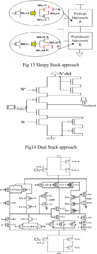
Fig 13 Sleepy Stack approach
Fig14 Dual Stack approach
Fig15 Full adder circuit using Dual stack approach
IV. SCHEMATIC DESIGN AND
SIMULATION RESULTS OF FULL ADDER CIRCUIT
I. Schematic design for Basic full adder circuit
International Journal of Computer Techniques -– Volume 4 Issue 6, 2017
ISSN :2394-2231 http://www.ijctjournal.org Page 77 Fig16 Digital schematic design for basic full adder circuit
Fig17 Layout for basic full adder circuit
Fig18 Simulation results for basic full adder circuit
J. Schematic design for Design-1 circuit
A schematic view of a design-1 full adder is shown in the figure 19. The layout and simulated input and output waveforms are shown in the figure 20 and 21 respectively.
Fig19 Digital schematic design for design-1 full adder circuit
Fig20 Layout for design-1 full adder circuit
Fig21Simulation results for design-1 full adder circuit
K. Schematic design for Design-2 circuit
A schematic view of a design-2 full adder is shown in the figure 22. The layout and simulated input and output waveforms are shown in the figure 23 and 24 respectively.
Fig22 Digital schematic design for design-2 full adder circuit
Fig23 Layout for design-2 full adder circuit
Fig24 Simulation results for design-2 full adder circuit
L. Schematic design for Sleep method circuit
ISSN :2394-2231 http://www.ijctjournal.org Page 78 layout and simulated input and output waveforms
are shown in the figure 26 and 27 respectively.
Fig25 Digital schematic design for full adder circuit using sleep method
Fig26 Layout for full adder circuit using sleep method
Fig27 Simulation results for full adder circuit using sleep method
M. Schematic design for Dual-Stack method circuit
A schematic view of a full adder circuit using dual-stack method is shown in the figure28.
The layout and simulated input and output waveforms are shown in figure 29 and 30 respectively.
. Fig28 Digital schematic design for full adder circuit using dual-stack method
Fig29 Layout for full adder circuit using dual-stack method
Fig30 Simulation results for full adder circuit using dual-stack method
V.CONCLUSION
In this thesis, low leakage 1 bit full adder cells are proposed for mobile applications with low leakage power. By using the proposed technique leakage power is reduced by 33% (Design1), 46% (Design2) in comparison to the conventional adder cell (Base case). By using the novel techniques of sleep method and dual-stack method leakage power is further reduced when compared with the basic circuit, design-1 and design-2 circuits. In this thesis, we have presented different ways to reduce the leakage power of one-bit full adder circuits.
One-bit full adder circuit is considered as two cascaded blocks i.e. carry generation block and sum generation block. Separate sleep transistors are added at the bottom of the blocks.
To summarize, since full adder circuits are designed in five different methods, each with its own advantages and disadvantages of power, area, etc,. can be used depending up on the requirement of the designer.
REFERENCES
1. Radu Zlatanovici, Sean Kao, Borivoje Nikolic, “Energy-Delay of Optimization 64-Bit Carry- Lookahead Adders With a 240ps 90nm CMOS Design Example,” IEEE J. Solid State circuits, vol.44, no. 2, pp. 569-583, Feb. 2009.
International Journal of Computer Techniques -– Volume 4 Issue 6, 2017
ISSN :2394-2231 http://www.ijctjournal.org Page 79 3. Rabaey J. M., A. Chandrakasan, B. Nikolic, Digital Integrated
Circuits, A Design Perspective, 2nd Prentice Hall, Englewood Cliffs, NJ, 2002
4. Pren R. Zimmermann, W. Fichtner, “Low-power logic styles: CMOS versus pass-transistor logic,” IEEE J. Solid- State Circuits, vol. 32, pp. 1079–1090, July 1997.
5. S.G.Narendra and A. Chandrakasan, Leakage in Nanometer CMO Technologies. New York: Springer-verlag, 2006.
6. K.Bernstein et al., “Design and CAD challenges in sub-90nm CMOS technologies,” in Proc. int. conf. comput. Aided Des., 2003, pp.129-136.
7. “International Technology Roadmap for Semiconductors,” Semiconductor Industry Association, 2005. [Online]. Available:http://public.itrs.net
8. H.Felder and J.Ganger,”Full Chip Analysis of Leakage Power Under Process variations, Including Spatial Correlations, “in proc. DAC, pp.523-528, June2005.
9. Jun Cheol Park and Vincent J. Mooney” Sleepy Stack Leakage Reduction” IEEE transactions on very large scale integration (vlsi) systems, vol.14, no.1. november 2006.
10. Harmander Singh, Kanak Agarwal, Dennis Sylvester, Kevin J. Nowka,” Enhanced Leakage Reduction Techniques Using Intermediate Strength Power Gating,” IEEE Transactions on VLSI Systems, Vol.15, No.11, November2007.
11. Y.Chang.S.K.Gupta, and M.A.Breuer,”Analysis of ground bounce in deep sub-micron circuits”, in proc.15th IEEE VLSI Test symp. 1997, pp110-116.
12. N.West. K.Eshragian, Principles of CMOS VLSI Design: A systems Perspective, Addison-wesley, 1993.
13. Suhwan Kim, Chang Jun Choi, Deog-Kyoon Jeong,Stephen V. Kosonocky, Sung Bae Park,” Reducing Ground-Bounce Noise and Stabilizing the Data Retention Voltage of Power-Gating Structures,”IEEE transactions on Electron Devices,Vol.55,No.1,January2008.
14. S.Mutoh et al., “1-v power supply high-speed digital circuit technology with multithreshold-voltage CMOS.”JSSC, vol.SC- 30, pp.847-854, Aug.1995.
15. Charbel J. Akl, Rafic A. Ayoubi, Magdy A. Bayoumi, “Aneffective staggered phase damping technique for suppressing power-gating resonance noise during mode transition,” 10th
International Symposium on Quality of Electronic Design, pp.116-119, 2009.
16. K. Kawasaki et al., “A sub-us wake-up time power gating technique with bypass power line for rush current support,” IEEE J. Solid-State Circuits, vol.44, no. 4, pp.146–147, Apr. 2009.
17. Ku He, Rong Luo, Yu Wang, “A Power Gating Scheme for Ground Bounce Reduction During Mode Transition, ” in ICCD07, pp. 388-394, 2007.