University of Warwick institutional repository:
http://go.warwick.ac.uk/wrap
A Thesis Submitted for the Degree of PhD at the University of Warwick
http://go.warwick.ac.uk/wrap/73862
This thesis is made available online and is protected by original copyright.
Please scroll down to view the document itself.
RESEARCH IN MICROWAVE ELECTRONICS
-by-M. K. McPhun, B.Sc., -by-M.I.E.E., C~Eng.
A thesis submitted for the degree of Doctor of Philosophy
at the 'University of Warwick, England, May 1974.
BEST COpy
AVAILABLE
Abstract
The thesis
is a presentation
of publ~shed
work with
a commentary.
I
The 25 publicatio~cover
the period
from
1961 to 1974,
and with one exception
(on the subject
of
silicon
transistor
circuits)
are in the general
area of
microwave
electronics.
Work
on tunnel
diode
amplifiers
includes
a stability
criterion,
a measurement
technique,
a:nplifier designs
for U .H.F.• and X-band
frequencies,
and application
to
short
hop radio-relay
systems,
(;eneral purpose
computer
programs
for the analysis
of
I
microwave
circuits
are discussed.
T~e method
of using
I
chain matrices,
which
has since found 0ide
application,
is presented.
work
on microwave
integrated
circuits
is presented
':"
.
wh
i
ch is mainly
concerned
w~
th measurement
techni ques ,
and mate~ial
and co~ponent
,properties.
r,1easurement
tec hni ques are pre sented for thin
dielectric
films,
rectangular
dielectric
plates,
thin conductin~
met~l
films,
and overla~capacitors.
In each case microwave
2
.Declaration
The research
discussed
in sections
2.1.,
2.2. and part
of sections
2.3. and 2.4. was done prior
to registration
for the Ph.D.
while
I
was employed
by the U.K.A.E.A.,
the C.E.G.B.,
and Mul1ard
Research
Laboratories.
This work was
solely
mine
except where
acknowledged.
The contributions
of respective
authors
to joint
papers
are made
clear in the text.
The remainder
of sections
2.3. and 2.4. discuss
research
done ,subsequent
to registration.
This was
carried
out at
the University
of Warwick
in the course
of my work
as .a lecturer
whilst
supervising
the research
students
who
appear
as co-authors
of
the papers
submitted.
In this work
I have been
an ~ctive
participant,
suggesting
projects
and obtai~ing
the necessary
facilities,
engaging
in regular
di~cussions
and contributing
solutions
to problems,
and
contributing
to and editing
the published
papers.
Further
details
of the contributions
made by others
is given
in the Acknowledgements
3
Acknowledgements
At U.K.A.E.A.,
Capenhurst
(now at Risley) I had many useful
discussions with my group leader D.F. Davidson who introduced
the
work on silicon transistors, and with my colleagues E. Harrison,
I
H. Jones; G. McGonigal, P. Roach, and A. Stead.
At C.E.R.L. Leatherhead
my
group leader J. Hooper inspired
the work on tunnel diode repeaters.
He and
my
colleagues
S. Hartley, D.L. Hedderly, N. Prewitt, F. Pullen, and B.J. Terry
all conttibuted
to useful discussions.
At Mullard Research Laborato.ries, Salfords
;1
was very
grateful to
my
group leader C.S. Aitcheson
for his perceptive
I
and constructive
criticism and the freedom he gave me, and to
my
colleagues J. Bandler, R. Davies, S.R. Longley,
B.H.
Newton,
,
D.A.E. Roberts, K. Tweedale
and J.F. Wells for mdny valuable
discussions.
At this time
I
also received usefJl advice from
C.A.P. F6xall and his colleagues at A.S.M. Wembley
(now part of
G.E.C.).
I
am especially grateful to F .C. de Ronde of Philips
Research Laboratories,
Eindhoven
for his advice on microwave
measurement
techniques and mechnical design, and for his
personal interest and encouragement.
4
programs and drafts of joint papers.
All
my
ideas have been
;
subjected to their criticism, and much of the work and the
solution$ have arisen out of group discussions.
J. Kelland, a
final year undergraduate
made a vital contribution
at a critical
time by commisioning
our microphotography
facilities.
I am
indebted to P.J. Smith for his painstaking work on the design
and construction of a great variety of precision mechanical
apparatus, and for contributing
ideas on new con~truction
techniques.
H.V. Shurmer, S. Novak, J.M. Duckett, and E.G.
Coates wdrked on setting up the Automatic Network A~alyser
and contributed
to valuable discussions.
The research at Warwick was supported byS.R.C.
grants
B/SR/3536 and B/SR/92l0,
grants from the Clarksort Foundation
and G.E.C., and a contract with R.R.E.
Support for research
students was given by the S.R.C., Microwave Assodiates
and
Redac Software Ltd.
I am grateful to Professor A.L. Cullen
,
who was
a
most helpful referee for the S.R.C.
I have also had
useful discussions with G.J. Hill of E.R.A., Leatherhead;
Professor
I.M. Stephenson and B. Easter of University College
of North Wales, Bangor; J. Curran and J. Twistleton
of G.E.C.
Wembley, and R.F. Mayo of G.E.C. Stanmore
(now at Lancaster
University).
Mullard Research Laboratories
and the Plessey
Company have been unstinting
in their cooperation with helping
me set up the processing
facilities at Warwick.
Professor O.W. Memelink for providing the hospitality
of his
group and arranging for me to use the library and computing
facilities.
In the course of the 14 years covered by this thesis there
are many people not mentioned
above who also have helped me.
To them
i
am grateful and I am sorry that neither space nor
my memor1 permit me to name them all.
I am most grateful to
Professor J.A. Shercliff. chairman
'I ,
of the Department
of Engineering.
and Professor J.L. Douce for
giving m~ such a free hand to develop microwaves :as a major
'activity at Warwick. and making available a generous share of
the available resources •
.
It is with regret that I record the death of Professor
F.J. Hyde, my first supervisor. who encouraged me to take up
this work at Warwick.
I am
grateful to Professor J.L. Douce.
Imy
present supervisor for negotiating
the research grants with
the ClarKson Foundation and G.E.C., and for advice on the
preparation of this thesis.
6
CONTENTS
2.1.
Direct Couping of Circuits using
Silicon Transist~rs.
Paee
2 .
3
6
9
11
11
Declaration.
Acknowledgements.
Contents.
1.
INTRODUCTION
2.
COMMENTARY ON PUBLICATIONS
2.2.
Tunnel Diode ~~p1ifiers.
11
2.2.1.
Future work.
14
2.3.
Computer analysis
.o
r microwave circuits.
14
Future work.
15
2.4.
Microwave Integrated Circuits.
16
2.4.1.
Material measurements.
17
I
2.4.1.1.
Future work.
18
Component measurements.
19
2.4.2.1.
Future work.
20
CONCLUSIONS.
22
---?
5.
APPENDICES
A.l. ~ome advantages of silicon transistors in
circuit design.
A.2.
Operation of the tunnel diode above the resistive
cutcff frequency.
A.3. Proposals for a 2-way tunnel diode repeater using
a 4-port circulator.
A.4. Practical stability criterion for tunnel-diode
circuits.
A.5. Practical stability criterion fortunnel~diode
circuits.
A.5. Measurement of negetive resistance using a
Z-g
Diagraph.
A.7. U.R.F. tunnel-diode amplifier.
A.8. Short-hop radio-relay systems using tunnel-diode
repeaters.
I'A.9. A tunable X-band tunnel diode amplifier.
A.IO. Comparison of TD~ with waveguide-below-cutoff
resonators.
A.ll. Microwave amplifier.
A.12. Variabie~impedancetransmission~line,device.
A.13. Tunnel-diode amplifiers.
A.14. A computer programme for the analysis of
8
A.15.
Automatic
general-purpose
microwave
circuit
analysis
programs.
A.16.
A study of lumped
components
for microwave
inte:;rated circuits.
A.17.
~licrowave measurement
of thin film
dielectric
properties.
A.18.
A microwave
relaxation
phenomenon
in
electron-beam-evaporated
films
of SiO.
A.19.'
Thin film
dielectric
measurements.
A.20.
Measurement
of the properties
of rectangular
plates
using
a rectangular
cavity.
A.2l.
Surface-resistance
measurements
of thin
conducting
films
at 10 GHz.
A.22.
Simple
resonator
method
for measuring
dispersion
of microstrip.
A.23 •.
Calibration
of microwave
~etwork
analyser
for
\
computer-corrected
s parameter
measurements.
,
A.24.
Measurement
of overlay
capacitors
at X-band
with
independent
assessment
of thin-film
conductor
losses.
A~25.
The effect
of parasitics
on the "des1gh of
9
1.
INTRODUCTION
This
thesis
is a presentation
of published
work,
with
a.
commentary.
Each
paper
is presented
as a separate
appendix
labelled
and referenced
A.l.,
A.2.
etc.
They
are presented
in
logical,
not chronologicsl
order.
Diagrams
are referenced
as
Fig. A.2.S.
for instance,
meaning
Fig.
S of appendix
A.2.
Chapter
2 is a commentary
on the papers,
which
is divided
~
.
into four sect~ons.
Sections
2.1., 2.2.,
and parts
of sections
2.3. and 2.4. discuss
research
carried
out at the U.K.A.E.A.,
C.E.R.L.
and Mullard
Research
Laboratories.
The remainder
of
section
2.3. and most
of section
2.4. cover
research
carried
out
at the University
of Warwick.
The following
historical
preview
will
show the connection
between
the papers.
Section
2.1. on silicon
transistors
and
circuits
stands
on its own.
The research
was
done at the U.K.A.E.A.
Central
tnstrumentation
Laboratory
while
I was working
on the
control
of industrial
processes.
All
the other
papers
deal with
aspects
of microwaves.
Section
2.2. deals with
tunnel
diode
amplifiers.'
I set up this work
in the U.H.F.
band
at C.E.R.L.
and later moved
to Mullard
Research
Laboratories
to extend
the
work
to X-band.
The work
on solid
state
amplifiers
at X-band
was
found
to be very dependent
on the parasitics
of the packages
in which
the active
devices
were
mounted.
Evidently
there
I
was
a need
to integrate
the active
device
chips with
the passive
10
I started
this work
at Mullard's
and then moved
to ~he
University
of Warwick
and set up facilities
for more
fundamental
work
on
lumped
component
M.I.Cs.
This became
my major
research
topic
at Warwick.
The research
on the computer
analysis
of
microwava
circuits
arose naturally
out of the work
on amplifiers.
I wrote
the first program
at Mullard's
because
I needed
to
calculate
frequency
responses
frequently.
This program
evidently
filled
a need of other workers,
and at the University
of Warwick
I extended
this work
to form a research
project
in
11
2.
COMMENTARY
ON PUBLICATIONS.
2.1.
Direct
Coupling
of Circuits
Using
Silicon
Transistors.
The research
described
in appendix
A.l. was
done before
silicon
transistors
were
in common
use.
Silicon
integrated
circuits
(S.I.Cs) were
in the process
of being
invented,
but
methods
of isolating
collector
regions
of S.I.Cs.
were
not
available.
The paper
describes
new circuit
techniques
~vailable
for use
with
silicon
transistors,
in particular
the possibilities
of
direct
coupoing.
These
techniques,
e.g. Fig.
A.l.8.
have
since
become
universally
accepted
and are normally
used
in S.I.Cs.
The basic
amplifier
circuit
of Fig. A.l.4.
is now used as a
,
1 2 '
basic
design
example
in undergraduate
texts
'..
I presented
this, pap~r
at three
I.E.E.
centres
where
I advocated
the use of
the amplifier
circuit
of Fig. A.l.4.
in S.I.Cs.
when
the collector
isolation
problem
had been
overcome.
This
circuit
was
in' fact
later adopted
for the Mullard
S.I.C.
type TAA 263.
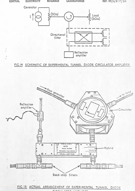
2.2.
Tunnel
Diode
Amplifiers.
Part
of the work
of the C.E.R.L.
Telecommunications
Group
led by
J.
Hooper
was directed
towards
establishing
short hop
microwave
repeater
links
(A.8.).
A suitable
frequency
band
for
operation
of these
links was
20 GHz to 30GHz.
but
solid
state
12
.
Tunnel
diodes
were
just becoming
available
and could be used
for
amplifiers
at the lower microwave
frequencies.
A number
of
workers
were
exploring
ways
of using
the tunnel
diode
at much
higher
frequencies,
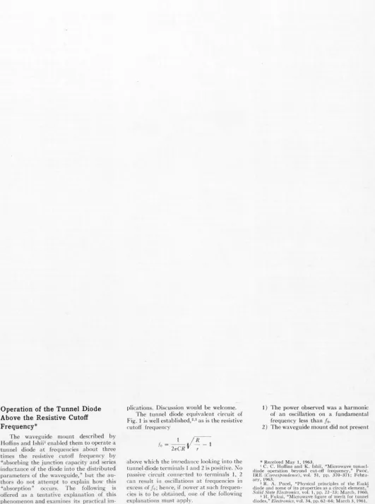
and A.2.
is part of that exploratory
work.
Hoffins
and Ishii's
reply
is most unsatisfactory
but
I did not
persue
the discussion
in public.
We had on hand
a requirement
for a repeater
link at a
frequency
of
470
MHz.
This was
for the North-West· of Scotland
where
a battery
powered
solid-state
repeater
was
called
for.
Preliminary
work
at
470
MHz demonstrated
the feasibility
of
using
a tunnel
diode
repeater
for this purpose,
and I put forward
the proposals
of A.3.
These
proposals
were
accepted
and funds
provided
for the development
of a 2-way
repeater
at
470
MHz,
and
field
trials.
The
tunnel
diode was
the first wide-band
negetive
resistance
device;
it presents
at its terminals
an impedance
with
a real
part which
is negative
over
the frequency
range
from zero to the
resistive
cutoff
frequency
f
, and f
is typically
a high
ro
ro
microwave
frequency.
All workers
in the field were hampered
by
undesired
oscillations
and lack of suitable
measurement
techniques.
Suitable
stability
criteria
did not exist
for these
essentially
nonlinear
negative
resistance
devices
used
in conjuction
with
distributed
circuits.
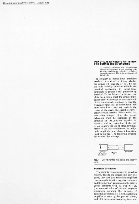
The
stability
criterion
I
evolved
and
subsequently
used
in
this work
is describea
in A.4.
and
A.5.
The new measurement
technique
described
in A.6.
is equally
suitable
for use with
the Hewlett
Packard
Network
Analyser
system
13
The heart
of the
470
MHz
repeater
consists
of
~wo
identical
reflection
amplifiers
which
are described
in A.7.
These
tunnel
diode
amplifiers
were
the first
to incorporate
independent
control
of diode bias
point,
gain,
and centre
frequency
respectively.
The whole
repeater
project
is described
in A.8.
J.
Hooper
and
I carried
out the theoretical
systems
work,
I designed
the repeaters
and planned
the field
trials
initially,
and D.L.
Redderly
developed
the repeaters
and carried
out
the field
trials,
later
taking
over
the whole
project
when
I left C.E.R.L.
i~ 1964.
Subsequent
work
at C.E.R.L.
on short-hop
repeater
systems
has been
successful,
and such microwave
links
are now being
assessed
in
I
full-scale
field
trials
by the C.E.G.B.
The main
recommendations
of A.8. have withstood
the test of time
and been
adopted
by the
3
Post
Office
for their
current
work
on short
hop repeater
systems
•
My work
at Mullard
Research
Laboratories
was
directed
towards
extending
the upper
frequency
limit
of tunnel
diode
amplifiers
so
\
as to produce
useful
amplifiers
in X-band.
The resulting
amplifier
uses
similar
design
techniques
to those
of A.7.
and is
described
in A.9.
and A.ll.
It was
exhibited
at the Physics
Exhibition,
Alexander
Palace,
in 1966.
This
amplifier
was
uniquely
simple
to use;
it was normal
practise
at that
time for
X-band
tunnel
diode
amplifiers
to have
a multitude
of tuning
screws with
an elaborate
setting-up
proceedure.
The
amplifier
gain
is controlled
by a transmission
line of variable
characteristic
impedance.
This
technique
is further
described
in A.lO.
and A.12.
Design
criteria
for' tunnel
diode
~mplifiers,
and the state~
of-the-art
in 1968 are summarized
in A.13.
Section
7.2. of
14
2.2.1.
Future
work.
The stability
criterion
of A.4. has
still not been
derived
theoretically,
and this would
be worth
doing.
This
criterion
could probably
be applied
also
to other negative
resistance
devices
such as Gunn and avalanch
diodes,
which
have
superseded
the tunnel
diode
as the main
solid-state
amplifying
elements
for
microwave
frequencies.
2.3.
Computer
Analysis
of Microwave
Circuits.
In the courseof
the work
on tunnel
diode
reflection
amplifiers
it was
frequently
necessary
to compute
frequency
responses.
Initially
programs
to do this for particular
circuits
(A.7.) were
written
to
my
specifications
by the C.E.G.B.
computing
department.
Later
at Mullard
Research
Laboratories
I wrote
the general
purpose
program
described
in A.l4.
in whi"ch the circuit
topology
is defin~d
by
the input data.
The method
is based
on 2-port
chain matrices
of networks
which
are cascaded
or connected
at tee
junctions.
This was
the first work
of this
type.
The program
was
further
developed
and used
in the U.K. by Mullards,
the Post
Office,
and the Plessey
Company.
In the U.S.A.
the method
was
4
5
adopted
by R.C.A.
and Sanders
Associates
Further
philosophy
of computing
applied
to microwave
circuits
is given
in A.1S.
These
desirable
features
of interactive
programs
using
a graphical
display
were
implemented
at th~
University
of Warwick
by
Marc ent
h6
un er my euperva ei.on,
d •• ~!. ! He
15
shows
that for microwave
circuits
the chain matrik
technique
,
.
is fastest
even for highly
interconnected
circuits6•
The
disadvantage'of
this technique
is that it cannot
be used
for
circuits
containing
interactive
loops,
e.g. bridge
types of
interconnections
cannot
be solved.
Marchent
invented
a new
mixed
matrix
method
of analysis
capable
of handling
any network,
with
a reasonably
short
computation
time 6,7.
He also rewrote
the chain matrix
analysis
program
in a form
suitable
for
inter-active
computing.
Animportant
aspect
of this work
is that the
computer
sorts out the network
topology,
and decides
the sequence
6
of computation
required
Most
of this work
awaits
publication.
2.3.1.
Future
work.
Any work
on the computer
optimisation
of microwave
circuits
(A.1S.) requires
~ suitable
general
purpose
analysis
program
at
its heart.
High
speed
in ,this case
is a prime
requirement
so
the chain matrix
method
is very
suitable.
There
remains
the need
to solve
the problem
of its use for circuits
containing
interactive
loops.
It is proposed
that the chain mat~ix
analysis
be used
to reduce
the circuit
to its simplest
possible
form.
This would
consist
of single
2-port
networks
interconnected
at junctions
to
form interactive
loops.
A typical
microwave
circuit
would
be
most
unlikely
to have more
than 10 junctions
left.
The
solution
would
then be automatically
continued
to completion
using Marchent's
mixed
matrix
method.
This would
be fast as the number
of
junctions
would be
small.
The concept
is very
simple,
but
implementing
it presents
difficult
problems
of topology.
Further
work
on incorporating
a range
of waveguide
and
16
would
considerably
increase
their usefulness.
2.4.
Microwave
Integrated
Circuits.
The performance
of solid-state
diodes
in X-band
is critically
dependent
on the parasitics
of the diode packages.
At Mullard
Research
Laboratoties
we
learnt
to live with
these parasitics
d
h
..
1
8
an
use
t em as Circuit
e ements
•
However
the parasitics
remained
the limiting
factor
in determining
the hig~
frequency
performance
of many
circuits.
There was
an evident
need
to
integrate
the semiconductor
chips with
the passive
microwave
components,
i.e. to make hybrid
microwave
integrated
circuits
(M.l.Cs.) •
The package
parasitics
are effectively
minute
lumped
components
even at microwave
frequencies.
Typical
values
are
inductance
in the range 0.1
to 1.0 nH and capacitance
in the
range 0.1 to 1.0 pF.
These
values
are suitable
for use as
lumped
components
at microwave
frequencies.
I investigated
the
likely
dimensions
of such lumped
components
made by means
of thin
films
deposited
on insulating
substrates,
and·concluded
that they
could be made
easily
using
the photolithographic
techniques
developed
within
the semiconductor
industry.
I put forward
proposals
to Mullard's
to start work
on lumped
component
M.I.Cs.
Before
the proposals
were
accepted
I was
committed
to move
to the
Univer.sity of Warwick.
However
before
leaving
Mullard's,
J.F. Wells
joined
me to make
the first
lumped
component
M.I.Cs.
(A.16).
The work
at Mullard's
continued
after
I left,
concentrat-9
ing mainly
on applications
I set up facilities
at the
University
of Warwick
with
the aid of a grant
from
the S.R.C.
and concentrated
the ~ork
on material
and component
properties
17
for lumped
component
M.I.Cs.
The properties
of thin films
at microwave
frequencies
were
quite
unknown
at that time,
and no suitable
measurement
techniques
existed.
Neither
were
there measurement
techniques
available
for
the minute
lumped
components,
and even micros trip measurements
were
confounded
by transition
discontinuities.
Hence
much, of
the work was
involved
with
measurement
techniques.
Thorough
surveys
of the available
materials,
substrates,
processes,
and
construction
techniques
for M.I.Cs.
have been
made by my
research
students
10,11,16,2?
2.4.1.
Material
measurements.
Considerable
effort
was
devoted
to developing
a cavity
technique
for the measurement
of thin dielectric
films.
The method
is
10
described
in A.17
and A.19
and full details
are given by Mehmet
Noteworthy
is the equivalent
circuit
method
of calculating
the
i
loss of the films
from
the cavity
return
loss at 'rescnance ,
This
is simpler
and more
accurate
than calculating
the film
loss from cavity
Q
measurements.
rhis method
wa~
also used by
Butlin
11 to optimise ,the r.f.
sputtering
process
for depositing
5i02 films.
Some new results
for thin films
of SiO are given
in A.1S.
A comprehensive
review
of the subject
of thin film
dielectric
measurements
is given
in A.19.
In order
to verify
the cavity
technique
of A.17.
for thin
films we developed
an independent
method
of measuring
self-supported
thin sheets
of dielectric
in a rectangular
waveguide
cavity
10.
We later
applied
this
to the examination
of the
18
from the substrates.
This work was done under
contract
to
12
R.R.E.
and later used by them
•
The method
is described
in
A.20.
Subsequently. I assisted
E.R.A.
to set up the same
measurement
technique,
and it is now their
standard
method
of
assessing
M.I.C.
substrate
materials
13 •.
,
A method
for measuring
conducting
thin films 'was needed
for
assessing
conductor
losses
in microstrip
transmission
lines and
thin film capacitors.
We evolved
the cavity
technique
described
,
21
d f
h
d
'1
'b
B
Li
11,
ln A ••
, an
urt er
etals
are glven
y
ut ln
•
Again
the te~hnique
uses an equivalent
circuit
approach
yielding
a
better
accuracy
and simpler
measurement
proceedure
than if
Q
measurements
were
used.
We used
the method
to assess
plated
11
.
metal
films
,and
some results
obtained
are given in A.24.
2.4.1.1.
Future
work.
We are now in a position
to use our measurement
methods
to
assess new
techniques
for depositing
lower
loss dielectric
films.
The present
films are still
too lossey.
The r.fl sputtering
h'
P'
14 h
d f
1
1
.
l'
'd
1d
tec nlque
ltt
as use
or
ow
oss optlca
wavegul
es cou
well
give the required
results
and should be investigated.
I hope
to collaborate
further with E.R.A.
on dielectric
measurements
using
the technique
of A.20.
Animproved
cavity
has
already
shown promise.
It is desirable
to apply
the
equivalent
circuit
technique
of A.17.
to this work
also.
Further
,
exploration
of the applicability
to these measurements
of Lynch's
,
15 b
d'
l'
d!
~
relatlon
etween
le ectrlc
constant
an
tano at r.f. and
19
microwave
frequencies
should
be made.
Discussions, are also
in
progress
with E.R.A.
on the possibility
of applying
a microprocessor
to the control
of microwave
dielectric
measurements,
and the
\computation
of the results.
It should be possible
to adapt
the well-known
perturbation
formula
of A.19.
equation
2, into a form which
enables
the
equivalent
circuit
technique
of A.17.
to be used ~ith
any cavity.
2.4.2.
Component
measurements.
X-band
lumped
components
are typically
less than 0.5 mm
across,
and we have
spent much
effort
on developing
special
measurement
techniques
to overcome
the errors
caused
by the
transitions
to normal
measuring
equipment.
The most
satisfactory
so far is to .mount the lumped
component
in a microstrip
line
for measurement
purposes.
We therefor
needed
to know
accurate
parameters
for microstrip
lines,
and the new technique
we used
as a basis
for obtaining
these is described
in A.22.
Much
further
work
on characterizing
discontinuities
in micros trip
is described
by Mehmet
10 and Michie
16
The Hewlett
Packard
microwave
network
analyser
system
has
featured
prominently
in our work
on component
measurement.
The need
to correct
systematic
errors
both
in the instrument
and in the transitions
to the unknown
led me to propose
an on-line
system
of computer
correction.
Simultaneously
Hewlett
Packard
introduced
their
automatic
network
analyser
(A.N.A.),
but
it was
economical
for us to develop
our own using
the existing
computer
20
concentrate
on the special
facilities
we required ••
G.E.C.
seconded
H.V.
Shurmer
to the university
to work
on the A.N.A.
and support
was
also given by
the Clarkson
Foundation.
Later
I obtained
further
support
for
H.V.
Shurmer
from
the S.R.C.
who
also
supported
a programmer.
C
t17.18.19
a G.E ••
compu
er
•
Initially
the work
was
done using
The work
has now been
transfered
to a Sigma
5 computer
and is presently
supported
by another
S.R.C.
grant
awarded
to
H.V.
Shurmer.
A major
difficulty
has been
the
construction
of suitable
calibration
pieces.
require~
in order
to do measurements
at a reference
plane
within
microstrip.
This
has been
overcome
by obviating
the need
for a micros trip matched
load.
as described
in A.23.
In order
to measure
overlay
capacitors
they were
deposited
.
..
16
directly
1nto m1crostr1p
resonators
•
Again
the measurement
I
method
used
an equivalent
circuit
approach
and this is described
in A.24.
Critical
to the use of any measurement
technique
for
characterization
of capacitors
is a thorough
assessment
of the
effect
of the parasitics.
This
is described
in A.25.
which
also
presents
design
criteria
for lumped
overlay
capacitors
in X-band.
Further
details
are given by Michie
16
2.4.2.1.
Further
work.
We intend
to combine
the A.N.A.
with
the computer
circuit
analysis
work
of section
2.3. and static
optimisation
to produce
a very
powerful
system
for the C.A.D.
of microwave
circuits.
21'
capacitors
for use in X-band.
This
requires
considerable
technological
support,
and can only be undertaken
if sufficient
support
is forthcoming.
Work
is in progress
on the construction
and measurement
f·
1
d'
d
20
Th .
k'"
•
•
o
m1crowave
umpe
ln uctors
19wor
18USlng
a mlcrostrlp
test jig and the measurement
technique
of A.23.
This proceedure
will
also be suitable
for the rapid
characterization
of a wide
22
3.
CONCLUSIONS.
The published
work
is a record
of research
undertaken
during
the last 14 years,
with
one exception
the papers
being
in the
general
area of microwave
electronics.
During
the later half
of this period
5 research
students
have been
supervised
by the
23
4 )
REFERESCES
1.
D.L.
SHILLIHG
and C. BELOVE
"Electronic
circuits:
discrete
and integrated"
McGraw-Hill,
1968,
Ch 8.
2.
P.E.
GRAY
andC.L.SEARLE
"Electronic
principles
-physics,
models,
and circuits"
John Wiley,
19;9, Ch 15.
3.
T.R.
RONBOTHA:J
"Short hop radio
relay
ays
t'era
work
at 20 GHz"
Froc.
Microwave
73
Conference,
Brighton,
1973,
pp 112-116.
4.
°N.N.
PARKER
ttDIPl'JET,
,a general
distributed
parameter
network
analysis
progra'1l" I.E.E.E.
Trans.
MTT-l2,
8, pp 495-505.
5,
P.E. GP.EE~
"General
purpose
proe,:ramsfor the frequency
doraa
Ln
analysis
of microwave
circuits"
ibid..
P9
506-513.
s.
B.G. ~;~ARC::r..E~~T
"Interactive
computer
programs
for the
comnuter
aided
design
of linear ,microwave
circuits"
! I • •
PhD Thesis,
University
of Warwick,
1973·
7.
B .G. MARCT-tE~T "Computer
aided
design
of microwave
circuits"
.Froc. summer
School
on Circuit
Theory,
Kobylisy,
Czechoslovakia
(Sept, 1971).
8.
o.s.
AITCHESON,
R.DAVIES,
and C.D.
PAYNE
"A balanced
micropi1l-diode
para.'Tletric
amplifier
(which
supports
the Q-band
idling
current
in the series
resonance
of
t.he
varactor)"
Proceedings
of the 6t ~ international
conference
on Microwave
and Optical
Generation
and
A:nplification,
Cambridge,
September
19(=)6,I.E.E.
24
9.
C.S.
AITCHESON
et.al.
"Lumped-circuit
elements
at
microwave
frequencies"
I.E.E.E.
Trans.
MTT-19,
12,
pp 92S-937
(Dec. 1971).
10.
K.
1lliFr'.!ET
"lJicrowave integrated
circuits
- preparation
and measurement
techniques
for materials
and components"
FhD Thesis,
University
of Warwick,
1970.
11.
R.S.
BUTLIN
"Microwave
integrated
circuits-
preparation
and measurement
techniques
for metal
and dielectric
films"
PhD
Thesis,
University
of 7larwick, 1973.
12.
J
.R.
BOSliliLL
I'The effect
of the physical
properties
of alumina
substrates
on their
use in microwave
hybrid
circuits"
Microelectronics,
2,
lQ,
pp
33-39,
(1':171).
13.
G.J.
HILL
"Alumina
for microwave
applications"
in High Frequency
Dielectric
Measurement,
I.P.C.
Science
a~d Technology
Press
Ltd, pp 127~134,
(1973).
14.
C.~N.
PITT
"sputtered-glass
optical
waveguides"
Electronics
Letters,
2,
17, pp 410-403
(23rd Aug.
1973).
15.
A.C. LY~:CH
"Relationship
between
permittivity
and
loss
tan~~nt"
Froc.
I.E.E.,
118,
1, pp244-246,
(Jan.
1971).
! •
16.
D.
MICnIE
"~.!icrowaveintegrated
c ircui ts
-preparation
and. measurement
techniques
for overlay
capacitors"
PhD Thesis,
University
of W',lrwick,1974.
17.
H.V. SF.UR..,':ER
"Correction
of a S;nith chart
display
throug.h bilinear
transformations"
E1ect:ronics Letters,
25
18.
H.V. SHU&\!ER "New method of calibrating a network
analyser"
Electronics Letters,
6,
23,
pp
733-734,
(12th
Nov.
1970).
19.
H. V.
SHUR~rER
"Low-level programming for the
on-line correction of microwave measurerrlents" Radio
and Electronic Engineer
~,
8,
pp
357-364,
(Aug. 1971).
20.
E.F.
da SILVA
"Inductors as lumped elements in
L1icrowave integrated circuits"
MSc Thesis, University
A.l.
APPENDIX
1.
Some
advantages
of silicon
transistors
in
circuit
design.
THE INSTITUTION
OF
ELECTRICAL
ENGINEERS
FOUNDED 1871: INCORPORATED BY ROYAL CHARTER 1921
SAVOY
PLACE,
LONDON,
W.C.2
SOME ADVANTAGES OF SILICON TRANSISTORS
IN CIRCUIT DESIGN
By
M. K. McPHUN, B.Sc.(Eng.), Graduate
Reprint from
THE PROCEEDINGS
OF THE INSTITUTION.
VOL.108, PART B,
No.
41, SEPTEMBER
1961
621.382.3 the Institution of Electrical Engineers Paper No. 3671 M Sept. 1961
©
SOME ADVANTAGES OF SILICON
TRANSISTORS
IN CIRCUIT DESIGN
By M. K. McPHUN,
B.Sc.(Eng.), Graduate.
(The paper was first received 10th March, and in revised form 17th May, 1961.)
SUMMARY
After transistors had been used for industrial instrumentation within the Development and Engineering Group of the United Kingdom Atomic Energy Authority for some years, silicon transistors were adopted for general-purpose use, as they were expected to be more reliable than germanium transistors. Ithas since become apparent that they possess more advantages over germanium transistors than is generally recognized, or was thought at the time of their adoption. Ror example, direct coupling of transistor circuits is facilitated and the number of components required may be much reduced; the use of electrolytic capacitors may be avoided.
.The paper compares the performance of silicon and germanium transistors from the viewpoint of the circuit designer; physical origins of their characteristics are not discussed. A range of circuits which take advantage of the characteristics peculiar to silicon transistors is described. The circuits are for direct-coupled amplifiers, current amplifiers for small signals, switching applications and multivibrators with long periods.
(I) INTRODUCflON
Since the advent of silicon transistors, descriptions have been given of their use for special purposes, e.g. choppers' and low-drift input stages for d.c. amplifiers.P
Reliability is of prime importance in industrial control
equip-ment, particularly in the atomic energy industry. As soon as
an assured supply of silicon transistors became available, it was
decided to use them instead of germanium transistors for
general purposes in the Central Instrument Laboratory of the
U.K.A.E.A. (Development and Engineering Group) for the
following reasons:
(a) They were expected to be more reliable than germanium
transistors. .
(b) They could be operated at higher temperatures. than ger-manium transistors, a particularly useful feature in chemical plants.
(c) The manufacturers predicted that their costs would fall below those of germanium transistors within a few years, making germa-ruum transistors obsolescent for general purposes.
The paper deals with experience gained in using silicon
transistors for a wide variety of applications. The design of the individual circuits for these applications is not described in full
where the techniques used are conventional; only those points
of special relevance to the use of silicon transistors are described.
(2) COMPARATIVE PERFORMANCE OR GERMANIUM AND AVAILABLE SruCON TRANSISTORS
This discussion is concerned with transistor performance as it affects the circuit designer; the physical origins of the charac-teristics are not considered.
(2.1) Input Characteristics
The current/voltage curves for the emitter-base diode of
typical germanium and silicon alloy-junction transistors (Fig. 1)
show a sharper turnover for the silicon than for the germanium
Written contributions on papers published without being read at meetlngs are invited for consideration with a view to publication.
Mr. McPhun was formerly with the United Kingdom Atomic Eoeray Authority (Development and Engineering Oroup) a.ndisnow at the Central Electricity Research Laboratories.
'pROCEEDINGS I.E.E., VOL. 108,PART B,No. 41,SEPTEMBER 1961
0·5 GERMANIUM 0'4· SILICON 0·3 0·2 0'1 %f---~---n0~'2---~0'~4----~~~~---~O'8 Veb·VOLTS
Fig. I.-Typical characteristics of emitter-base diodes for alloy-junction germanium and silicon transistors.
transistor. As with the forward-biased silicon diode, the
forward voltage across the emitter-base diode may be
con-sidered as constant at 0·6 V. For applied voltages of less than 0·4 V the junction may be considered to be reverse-biased. This
forward bias necessary for conduction may not be ignored in
circuit design as often as it is with germanium transistors; it
may, however, be put to good use, as is shown throughout the
paper.
(2.2) Leakage Current and Temperature
The collector current flowing with open-circuit emitter is
much smaller for the silicon than for the germanium transistor.
This is the common-base leakage current, leo; the published
applications I, 2 of silicon transistors make use of the fact that leois very small so that its dependence on temperature has much
less effect on circuit performance than with the germanium
transistor. The effect of temperature on the leakage currents
is the same for both germanium and silicon transistors, Le. an
increase in temperature of about 9° C causes the leakage current
to double; Table 1shows typical figures for silicon and
ger-manium alloy-junction transistors.
In many general-purpose circuits the leakage current of the
silicon transistor may be completely neglected, thus obviating the need for stabilizing the d.c. working point against changes
in leakage current with temperature; this leads to simpler
circuits and greater reliability.
McPHUN: SOME ADVANTAGES OF SILICON TRANSISTORS IN CIRCUIT DESIGN
Table 1
COMPARISONOF LEAKAGECURRENTSAT 25° C FORGERMANIUM
AND SrLlCONTRANSISTORS
Description Type I,. I~o
IJ.A IJ.A
A.F. germanium OC71 5 150
R.F. germanium OC44 0·5 25
Silicon OC201 10-3 60x 10-3
The other main temperature effect is the variation of Vc ~
with temperature at constant collector current. This effect is
the same for both silicon and germanium transistors, being about
2·5mV per deg C.
The permissible range of operating temperatures is much
greater for silicon than for germanium transistors. Typical
maximum operating temperatures are germanium, 75° C and
silicon, 150°C.
(2.3) Collector Resistance
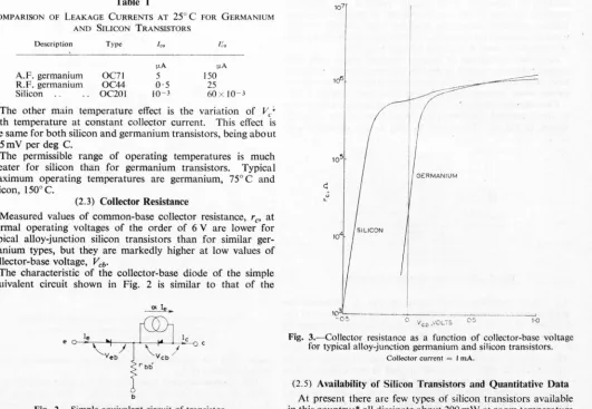
Measured values of common-base collector resistance, rc, at
normal operating voltages of the order of 6 V are lower for
typical alloy-junction silicon transistors than for similar ger-manium types, but they are markedly higher at low values of collector-base voltage, Vcb'
The characteristic of the collector-base diode of the simple
equivalent circuit shown in Fig. 2 is similar to that of the
b
Fig. 2.-Simple equivalent circuit of transistor.
emitter-base diode, Fig. 1. For normal operation as an
ampli-fier, the emitter-base diode is forward-biased and the
collector-base diode is reverse-biased. However, the silicon diode is
effectively reverse-biased for voltages through zero to forward values of a few tenths of a volt, and it would thus be expected that transistor action would be maintained with high collector
resistances for collector-base voltages in this range. This is
indeed so, as shown in Fig. 3 which gives measured curves ofrc
plotted against Vcbfor both germanium and silicon transistors.
Over the range 0·2 V reverse to 0'1 V forward for Vcb, the
collector resistance of the silicon transistor decreases by one-third while that of the germanium transistor decreases by three decades.
(2.4) Noise
Measurements! showed that the best type OC200 silicon
transistors were slightly less noisy than the best available
ger-manium transistors. The manufacturers claim the silicon OC20t
to have a lower noise figure than the OC200, and measurements
show a noise figure of 6 dB with a source resistance of 500
n
to be easily obtainable at t kc/s with the OC20I.
The OC20t was adopted for general-purpose usc, and
experience has shown that its noise figure is comparable with
that of the best available germanium transistors.
A lower noise figure is obtained by operating a transistor at very low values of collector current.? This is faciJitated with silicon transistors, as collector currents of 50 fJ.A or less may be
used in low-noise circuits without I'co proving troublesome;
und~r these conditions linearity may be a limiting factor.
571
--- ----...J
o Vcb ,vOLTS o s 1'0
Fig. 3.-Collector resistance as a function of collector-base voltage for typical alloy-junction germanium and silicon transistors.
Collectorcurrent=IrnA.
(2.5) Availability of Silicon Transistors and Quantitative Data At present there are few types of silicon transistors avai.lable in this country;" all dissipate about 200mW at room temperature
and have common-base cut-off frequencies between I and
4 Mc/s. The germanium transistors of similar size and
per-formance dissipate only 100mW at room temperature because
of their lower maximum junction temperature.
Silicon power and high-frequency transistors are now becoming available, but their price restricts their use to special applica-tions. The cut-off frequency of the alloy-junction silicon tran-sistors, however, has been found adequate for most instrument work, the exception being due to the difficulty in making stable
wide-band amplifiers with large amounts of overall negative
feedback.
So far a very large spread in the characteristics of silicon
transistors must be tolerated; values of the common-emitter
current gain IX' from 20 to 130 may be expected in a batch of
20 transistors. New types with a narrow spread of IX' have
recently become available, but even with these, values of IX'
may still be found in the range 30-75.
Quantitative information about silicon transistors is scarce, and this puts circuit designers at a disadvantage. Most charac-teristics must be measured by the user, and because of the large
spread this can be a very laborious process. For this reason,
most of the circuits described here will tolerate a very wide spread of transistor characteristics.
(3) DIRECT-COUPLED AMPLIFlERS
The frequent requirement for 50c/s servo amplifiers showed
the need for a.c. amplifiers using direct coupling between stages;
• A rapid increase in the variety of silicon transistors available has taken place
[image:33.565.23.554.40.407.2]572 McPHUN: SOME ADVANTAGES OF SILICON TRANSISTORS IN CIRCUIT DESIGN
electrolytic capacitors were usually required for interstage
coupling because of the low impedance of transistor circuits.
Greater reliability should be expected from amplifier circuits using no electrolytic capacitors, and any reduction in the number of components used should also increase reliability.
Amplifiers consisting of common-emitter stages with each
collector directly coupled to the base of the succeeding transistor have been suggested.i-> and practical examples of this type of circuit using germanium transistors have been described.1,4,5
Considerable advantages are gained by using silicon transistors
in direct-coupled amplifiers; the basic form of the circuit is
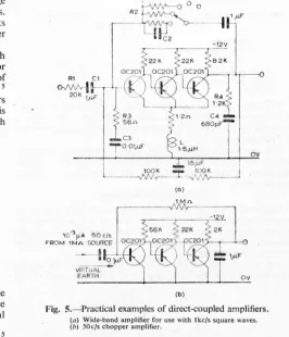
shown in Fig. 4. Transistors TI and T2 are operating with
[image:34.587.300.566.41.351.2]- Hr
---z--~
,-{)
i I VoI
ov WORKING POI~ STABILIZING LINEFig. 4.-Basic direct-coupled a.c. amplifier.
Veb =0, a condition shown clearly in Fig. 3. Whereas the
stage gain with germanium transistors is very low because of the low value of
'e
at V<b =0, that with silicon transistors is normal for the case where 't(l - a)>
RI•.Let us consider germanium transistors used in this circuit.'
The collector resistance is reduced to one-hundredth of the
value obtained with a few volts applied to the collector, then
'e(1 - 0:)
-<
RL, and this severely limits the gain per stage;moreover, under these conditions
'e
is very sensitive totem-perature, and so also is the stage gain. The voltage swing at a collector must be limited to the millivolt region because of the change in re with Veb' A voltage-divider coupling must be used to the last stage" in order to allow sufficient voltage swing at the base of T 3; this, in turn, means that a positive supply rail must be used.
With silicon transistors, a high value of re is maintained, and so RL
<
re(1 - a); the stage gain is not then limited by rcand the small variations in rc with Vcb have negligible effect. The maximum voltage swing at a collector may be of the order of 200 mV; this is sufficient to provide a signal at the T3collector
with a peak voltage of a few volts, hapositive rail being required for an interstage coupling. Further, as the stage gain is governed
by RL and not rc' any temperature-dependence of re does not
affect the gain.
Table 2.
EFFECT OF GAIN OFT ION Vo(FIG. 4)
v.
30 40 60 rnA 1/30 1/40 1/60 v 10 7·5 SThe simple operating-point stabilization shown in Fig. 4 Is
adequate for most purposes. The required base direct current,
Ib" of the first stage is determined; R is then chosen so that
Vo - V~b
=
Ibl R. Variations of 1;0 with temperature may be neglected as this current is so small; variations of VPbwithtem-perature are much less than VQ• Difficulty is encountered,
however, if it is desired to have a close control on Vo' and
at
theRl Cl
0VVVv1~
20K').lF
OV
l
.
15).lFI
---)5ZJ~--~-_v~~
(a)
(b)
Fig. 5.-Practical examples of direct-coupled amplifiers.
(0) Wide-band amplifier for lise with I kc/s square waves.
(b) 50c/s chopper amplifier.
same time to accommodate transistors demanding widely
differing values of 'bl• .
The solution adopted here is to have a close control on the
value of
a;
for the first transistor T,. For example, with'cl
=
I rnA, R =300 kil, the values shown in Table 2 will beobtained. The variations of
IX;
tolerated will be governed bythe permissible variation of Vo.
Practical examples of these circuits are shown in Fig. 5.
Fig. 5(a) shows a wide-band amplifier for use with I kc/s square
waves. Fixed current feedback is applied, and gains of 1,2,5,
10, 20 and 25 are obtained by switching the shunt feedback
resistors. Stabilizing networks R)C), R4C4, C2 and L are
necessary because of the large. degree of feedback and wide bandwidth of 100 kc/s.
For the low-noise chopper amplifier shown in Fig. 5(b) it was convenient to lise the same resistor for feedback at the 50c/s signal frequency as for stabilizing the d.c. working point. An electrolytic capacitor would have been required for decoupling a separate working-point stabilization loop at SOc/s.
(4) CURRENT AMPLIFIERS FOR SMALL SIGNALS
It is sometimes inconvenient to use an electrometer valve in
conjunction with equipment otherwise using transistors, usually because the power supplies required are hot available. Current amplifiers using silicon transistors have been successfully used in such applications and two examples are described.
Fig. 6 shows the circuit of a head amplifier for a photomulti-plier detecting very low levels of light chopped at 1 kc/s. Two
cascaded emitter followers .are used, giving a current gain of
about 300. The collector current of TIis set at 120!-LA. This
is a compromise between the low value required fOTlow noise and the need for linearity over a range of input currents of three
decades, from 10-8 to 10-1 IA peak. The noise generated in
[image:34.587.46.300.157.295.2]