A CONTROLLED CURRGNT INVERTER FOR ACTIVE DISTORTION
COMPENSATION
AND
POWER .FACTOR CORRECTION
Simon
D. ROUND
and
Richard M.
DUKE
Department of Electrical & Electronic En,$neering
University of Canterbury, Christchurch, New Zealand
Absrma.-
A technique of achieving both active w e n tdistortion compensation
and
power factor correction is describedA signal corresponding to the phase corrected distortion
component of load current is amplified by a high f r e p e n q asynchronous sivitching inverter for addition back to the mpply
current to cancel the load current distortion
and
to providepower_ factor correction Current distortion compensation and power factor correction can be provided either separate& or
combined to provide total compensation. Experimental results, illustrating the ystem's abiliry to reduce the current harmonic
distortion components
and
provide power factor correction, arepresented The design of an intelligent controller, using a TMS32OC30 digital Signal processor, for the compensm'on
system ir a150 discussed
Introduction
The detrimental effects of load current distortion and
poor power factor can be solved by removing the load current
distortion components and leaving a "clean" power factor
corrected sinusoid. Commonly this is achieved by the
addition of passive filters at the point of supply and shunt
capacitors connected across the load.
Passive filters are however, non-selective, so they not
only filter out the unwanted harmonic components from the
supply they are installed on, but they also serve as a "sink" for
the distortion components produced by other consumers in
the vicinity. They are also generally tuned to remove specific
frequency components and are therefore not a completely
satisfactory solution when the harmonic composition of the
distorted waveform changes. An active filter however is not
tuned to remove specific frequency components and can
provide varying amounts of distortion compensation to cater
for load changes.
Banks of power factor correction capacitors cannot
correct power factor for varying loads, they can provide total
correction only for a selection of loads. Active power factor
correction techniques can, on the other hand, provide total
correction for a continuously variable range of loads.
An
active compensation system has been developedwhich can directly cancel any unwanted current distortion and
at the same time provide power factor correction. The system
is based on current reinjection into the power supply using a
high frequency controlled current inverter configuration
as
developed for use in AC variable speed drives"2.
The Active ComDensation Svstem
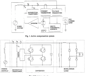
The active compensation system, which employs a high
frequency time based hysteresis controlled current inverter, is
shown in Fig. 1.
A sinusoid corresponding to the power factor corrected
fundamental component of load current (1,). which may be
comprised of fundamental and distortion components, is
extracted by the Signal Processing Unit (SPU)-. Digital
circuitry is used for synthetically generating the fundamental
component of I, from a look-up EPROM. Subtraction of this
power factor corrected fundamental component from I, leaves
the distortion component of load current, which is then
amplified by the controlled current inverter to form the
compensating current (I,). I, is then added to the supply via
a reinjection transformer. This results in distortion current
cancellation and a nearly sinusoidal power factor corrected
supply current
(Is).
Emenmental Verification
The active compensation technique has been evaluated
using a single phase prototype circuit that provides up to
I
Fig. 1 Active compensation system
. ,
. .
~ POWER ' '
;
SUPPLYj
~- ... - ... , . ,
NONLINEAR
[image:2.613.141.494.63.379.2]INVERTER LOAD
Fig. 2 Prototype circuit
load consists primarily of a resistive-inductive base load
combined with a typical single phase rectifier load. The
resistive and inductive components of the base load are rated
500 W and 900 VAr respectively and draw a combined
current of 6 A rms. The rectifier load is rated 300 W and
delivers 1 A DC. The power supply for both the active
distortion compensation system and the non-linear load is
provided at 240 V from a 50
Hz
system. The switchinginverter, which uses IGBTs, is interfaced to the power supply
via a reinjection transformer of ratio 2:l. The inverter output
current is sensed using a resistive shunt and the comparison
of inverter output current and compensating current signal
takes place referenced to the inverter output. The inverter
control logic activates either of the two diagonal pairs of
transistors, to apply a positive or negative voltage across the
iiansformer connected load. Compensating current then
ramps up or down at a rate determined by the time constant
of the reinjection transformer.
Switching strategy
With reference to the transistor switching diagram
(Fig.3), the transistor switching instants are determined in the
following way: Assuming the actual inverter output current is
greater than the compensating current signal (point A), a
negative voltage is applied across the transformer connected
load and the actual inverter current ramps down. This ramp
down of inverter current continues for t ps after crossing the
compensating current signal at point B. At point C the
INVERTER
COMPENSATING
: :
[image:2.613.325.527.505.646.2]INVERTER OUTPUT CURRENT
Fig. 3 Transistor switching diagram
\
',
1,
"4,
25 AJDN-,I
<I
,
'
alternate pair of diagonal transistors are activated and a
positive voltage is applied across the transformer connected
load. The actual inverter current now ramps up, continuing
past point D for t ps.
This
hysteresis time delay of t ps setsthe average switching frequency
(fv
=
1/4t) of the inverter. \40 m y c
(a) Load current
Clearly the actual switching frequency may vary over a wide
the required compensating Current varies. Hence the range !
0 sec
range when the hysteresis time delay is fixed and the slope of
' I
i
of transistor switching frequencies, which are asynchronous,
are determined by the required compensating current
waveform. I i
e f 2 0 -
6
Comuuter Simulation
Since the switching operations of the asynchronously
controlled current inverter cannot be prespecified a dynamic
state-space modelling technique is necessary. Such a state-
space formulation has been developed and verifiec? for
analysis of the active compensation system. Simulations
described i n this paper have been carried out using the
'MATLAB simulation and analysis software package.
Average Switching Frequency
-
2R79 kHzn
Performance
The performance of the active compensation system has
been assessed initially from the point of view of providing
supply current distortion compensation oply. Active power
factor correction
has
then been combined with distortionempensation to provide total compensation, producing a
unity power factor sinusoidal line current at the point of
supply.
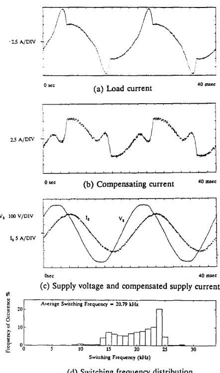
Distortion ComDensation
0 Y C (b) Compensating current 40mrec I
Svilching Frcquency ( W )
[image:3.620.306.527.64.438.2](d) Switching frequency distribution
Fig. 4 Distortion compensation
The distortion of the load current I, is evident from correction has been included along with distortion
Fig. 4(a) and the measured Total Harmonic Distortion compensation, the compensating current I, shown in
(THD), taking into account frequencies up to 1050 Hz, is Fig. 5(b), is quite different. The compensated sinusoidal
24.8%. The compensating current I, is shown in Fig. 4(b) Supply current I, and supply voltage V, are shown in Fig. 5(c).
and the compensated sinusoidal supply current I, In addition to the reduction in THD, from 24.8% in Fig. 5(a)
(THD 1.53%)
and
supply voltage Vs are shown in Fig. 4(c). to 4.3% in Fig. 5(c),I,
has been phase shifted by 55" and isSwitching frequency variability is apparent from the trace of now in phase with
V,.
The actual phase displacementI, in Fig. 4(b) and the distribution of these switching between
v,
and I, being less than 1".frequencies is shown in the computer simulation results of
Fig. 4(d). The range of switching frequencies extends from
7 kHz to 28 kHz with an average switching frequency of
21 kHz.
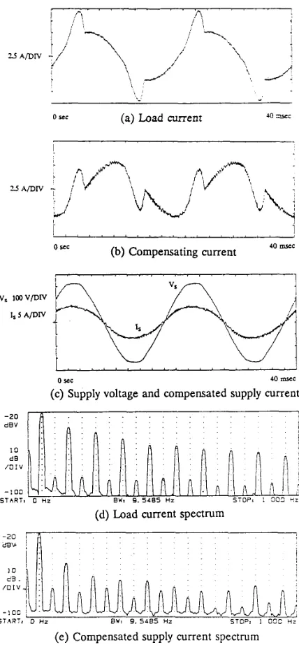
Total Comuensation
Figs. 5(d) and (e) show the spectra of I, and I,
respectively. With total compensation the 3rd harmonic
(150 Hz) has been reduced by 15 dBV and is now 28 dBV
below the fundamental (3.98% of the fundamental), while the
5th harmonic (250 Hz) has been reduced by 22 dBV and is
The load current I, shown in Fig. 5(a) is identical with now 40 dBV below the fundamental (1.0% of the
I '
0 sec (a) Load current U) -z!c
!
2 5 A D N
I , , . , , , , , , , , , . , , , j
(b) Compensating current 40 m x C
0 Y C
v, l W V / D I V
I, 5 A P N
0 Y C 40 m%C
(c) Supply voltage and compensated supply current
-20 I n 1
I
dBV
1 /:I
: ~ : , . . . .. . . .
10 dB / O I V
-100
STOP, 1 309 rz
S T A R T S 0 Hz Bur 9 . 5 4 8 5 H Z
(d) Load current spectrum
i
10
c3.
/ D I V
-!OS
S T t ? T z D HZ 0 W 9 . 5 4 8 5 Hz S T O P : 1 0 3 C Hz
(e) Compensated supply current spectrum
Fig. 5 Total compensation
Operating efficiency of the active compensation system
is based on the real power flow in the system and is
determined from the fundamental current that is in phase
with the supply voltage. Assuming that the compensation
system is supplied from a strong ac system, the real power
flow is the product of the voltage and in phase fundamental
current component. The efficiency
(0
of the compensationsystem can then be defined by
738
p l o d d current
' s u p p l y w e n t vi co.9Qnsa tion
C
,=Fig 6(a) shows the measured efficiency of the active
compensation sysrem with different average switching
frequencies and DC bus voltages when providing total
compensation. The efficiency improves with low bus voltages
because the rate of rise of current has decreased. The
switching frequency profile now contains a greater proportion
of lower frequency components. Hence the switching losses
decrease because the inverter is switching at a lower average
frequency and a lower bus voltage is applied across the
semiconductors. As the bus voltage is increased, for the same
average switching frequency, the semiconductor switching
losses increase significantly and efficiency decreases. At low
frequencies (less than 5 kHz) the hysteresis band is much
larger, thus the current excursions are increased and the
conduction losses of the system are dominant. At high
switching frequencies (greater than 20 kHz) the switching
losses of the system become more dominant and thus the
efficiency tends to fall. The most efficient average switching
frequency for this particular non-linear load is in the range
4
-
14IrHz.
To establish an appropriate bus voltage operatinglevel the THD performance of the compensation system must also be considered.
The level of supply current THD at various bus voltages
and average switching frequencies is shown in Fig. 6(b). At
low bus voltages the THD performance is poor because the
DC bus has insufficient stored energy to reinject enough
compensating current for complete harmonic cancellation and
power factor correction. By increasing the bus voltage the
system can better compensate for the harmonic distortion and
laging power factor, however, the incremental increase in
THD at higher bus voltages is small. The other factor that can
alter the THD performance is the average switching
frequency. At low switching frequencies (less than 9 IrHz) the
THD can be up to three times larger than that achieved at
higher frequencies. The reason for this trend is that at low
frequencies the hysteresis band is much larger and thus the
harmonic compensation is less then ideal. As the frequency
increases the inverter output current can follow the required
compensating current signal far more closely and thus the
harmonic content can be further reduced.
[image:4.622.94.308.62.533.2]n
70
>4
1
5 10 15 20 25
200v
__
280V-
360V-
Average Switching Frequency (kHz)
THD of Complete Distortion Compensation System
10 I \ 1
I
5 10 15 20 25
Average Switching Frequency (kHz)
Fig. 6 Performance characteristics
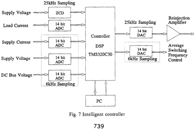
Intelligent Control
By changing the average switching frequency and the
DC bus voltage of the inverter an optimum operating point,
which achieves low supply current distortion at maximum
efficiency, can be reached. However with different types of
loads, this optimum operating point changes. Therefore an
intelligent controller, which monitors the efficiency and
distortion compensation performance, and alters the operating
point to achieve optimal performance, is proposed.
distortion signal to the inverter within 55 ps. Therefore a
sampling frequency of 25
kHz
is necessary and a high speedcontroller is required. To achieve real time operation, a
TMS320C30 Digital Signal Processor (DSP) has been chosen
as the controller. The hardware configuration of the DSP
distortion compensation system is shown in Figure 7.
The load current is sampled by a 14 bit ADC at
approximately 25.6 kHz. This sampling frequency is vaned so
that there are exactly 512 samples in each fundamental
The system has been designed to be accurate within one
degree of the fundamental (50 Hz). Thus the controller has
to measure I, subtract a sinusoid and send the resulting
period. The .variation in sample rate is necessary since the
fundamental frequency is not constant (variations of f 1%
may occur). The fundamental zero crossing is used to
25MJz Sampling
Supply Voltage
Load Current 14 bit
14 bit DAC
Average Switching Frequency
Supply Voltage Sampling Control
Supply Current
DC Bus Voltage 14 bit
ADC
6kHz sampling
[image:5.626.121.466.76.295.2] [image:5.626.136.462.489.710.2]synchronise the sampling frequency. Each load current sample
is sent to the DSP, where the instantaneous phase cerrected
sinusoidal value is subtracted, leaving the distortion signal.
The magnitude of the sinusoid is controlled by the voltage
level on the DC bus capadtors and the instantaneous load
current level, the resulting distomon signal is fed via a 14 bit
DAC to the inverter where it is amplified and reinjected into the supply.
Using a second 14 bit DAC the average switching
frequency is controlled in the range from 1 to 40 k H z Three
14 bit ADCs, sampling at a quarter of the sampling frequency
of the load current, are used to monitor the supply current
and voltage and the DC bus voltage. Using the supply voltage
information the system can perform power factor correction
and together with the load and supply current information
calculate the efficiency of the system.
Conclusion
It has been demonstrated that an active compensation
system using a high frequency asynchronously controlled
current inverter is effective in phase shifting and reducing the
harmonic content of distorted current waveforms. The novel
use of a digitally generated sinewave in the SPU has provided
an effective means for deriving the required compensating
signal for any arbitrary load current waveform. There is an
optimum ~. operating range for the active compensation system
which is determined by the choice of average switching
frequency (hysteresis time) and DC bus voltage of the
inverter. The design of an intelligent controller, which
monitors the efficiency and distortion compensation
performance and alters the operating point to achieve optimal
performance of the active compensation system, has also been
outlined.
References
[ l] Brod D.M. and Novotny D.W.: "Current control of
VSI-PWM inverters",
IEEE
Trans. 1985, IA-21,pp562
-
570.[2] Penny
J.R.:
"Modem controlled-current AC drives",Roc. of a seminar "Power Electronics", Annual Conf. of
IPENZ, 1987, Vol. 13, pp. 19
-
26.[3] Henderson K.C.: "The development of an active
harmonic filter for power systems", Proc. IPENZ Annual
Cod., 1990, Vol.II, pp.129
-
138.[4] Duke R.M., Round S.D. and Henderson KC.: "An
active filter for current distortion compensation in
power systems", Proc. 4th Conf. on Harmonics in Power
Systems, Budapest, Hungary. Oct.4-6 1990, pp.367
-
73.