Noise
Specs
Confusing?
AN-104
National Semiconductor Application Note 104 May 1974Noise Specs Confusing?
It’s really all very simpleÐonce you understand it. Then, here’s the inside story on noise for those of us who haven’t been designing low noise amplifiers for ten years. You hear all sorts of terms like signal-to-noise ratio, noise figure, noise factor, noise voltage, noise current, noise pow-er, noise spectral density, noise per root Hertz, broadband noise, spot noise, shot noise, flicker noise, excess noise, I/F noise, fluctuation noise, thermal noise, white noise, pink noise, popcorn noise, bipolar spike noise, low noise, no noise, and loud noise. No wonder not everyone understands noise specifications.
In a case like noise, it is probably best to sort it all out from the beginning. So, in the beginning, there was noise; and then there was signal. The whole idea is to have the noise very small compared to the signal; or, conversely, we desire a high signal-to-noise ratio S/N. Now it happens that S/N is related to noise figure NF, noise factor F, noise power, noise voltage en, and noise current in. To simplify matters, it
also happens that any noisy channel or amplifier can be completely specified for noise in terms of two noise
genera-tors enand inas shown inFigure 1 .
TL/H/7414 – 1
FIGURE 1. Noise Characterization of Amplifier
All we really need to understand are NF, en, and in. So here
is a rundown on these three.
NOISE VOLTAGE, en, or more properly, EQUIVALENT
SHORT-CIRCUIT INPUT RMS NOISE VOLTAGE is simply that noise voltage which would appear to originate at the input of the noiseless amplifier if the input terminals were
shorted. It is expressed in nanovolts per root Hertz nV/0Hz
at a specified frequency, or in microvolts in a given frequen-cy band. It is determined or measured by shorting the input terminals, measuring the output rms noise, dividing by am-plifier gain, and referencing to the input. Hence the term, equivalent noise voltage. An output bandpass filter of known characteristic is used in measurements, and the measured value is divided by the square root of the
band-width0B if data is to be expressed per unit bandwidth or per
root Hertz. The level of enis not constant over the
frequen-cy band; typically it increases at lower frequencies as shown
inFigure 2 . This increase is 1/f NOISE.
NOISE CURRENT, in, or more properly, EQUIVALENT
OPEN-CIRCUIT RMS NOISE CURRENT is that noise which
TL/H/7414 – 2
FIGURE 2. Noise Voltage and Current for an Op Amp
occurs apparently at the input of the noiseless amplifier due only to noise currents. It is expressed in picoamps per root
Hertz pA/0Hz at a specified frequency or in nanoamps in a
given frequency band. It is measured by shunting a capaci-tor or resiscapaci-tor across the input terminals such that the noise current will give rise to an additional noise voltage which is inx Rin(or Xcin). The output is measured, divided by
amplifi-er gain, refamplifi-erenced to input, and that contribution known to
be due to enand resistor noise is appropriately subtracted
from the total measured noise. If a capacitor is used at the input, there is only enand inXcin. The inis measured with a
bandpass filter and converted to pA0Hz if appropriate;
typi-cally it increases at lower frequencies for op amps and bipo-lar transistors, but increases at higher frequencies for field-effect transistors.
NOISE FIGURE, NF is the logarithm of the ratio of input signal-to-noise and output signal-to-noise.
NFe10 Log (S/N)in
(S/N)out
(1)
where: S and N are power or (voltage)2levels
This is measured by determining the S/N at the input with no amplifier present, and then dividing by the measured S/N at the output with signal source present.
The values of Rgenand any Xgenas well as frequency must
be known to properly express NF in meaningful terms. This
is because the amplifier inx Zgenas well as Rgenitself
pro-duces input noise. The signal source inFigure 1 contains
some noise. However esig is generally considered to be
noise free and input noise is present as the THERMAL NOISE of the resistive component of the signal generator
impedance Rgen. This thermal noise is WHITE in nature as it
contains constant NOISE POWER DENSITY per unit
band-width. It is easily seen from Equation 2 that the en2has the
units V2/Hz and that (en) has the units V/0Hz
eR2e4kTRB (2)
where: T is the temperature in§K
R is resistor value inX
RELATION BETWEEN en, in, NF
Now we can examine the relationship between enand inat
the amplifier input. When the signal source is connected,
the enappears in series with the esigand eR. The inflows
through Rgenthus producing another noise voltage of value
inx Rgen. This noise voltage is clearly dependent upon the
value of Rgen. All of these noise voltages add at the input in
rms fashion; that is, as the square root of the sum of the
squares. Thus, neglecting possible correlation between en
and in, the total input noise is
eN2een2aeR2ain2Rgen2 (3)
Further examination of the NF equation shows the relation-ship of eN, in, and NF. NFe10 logSinx Nout Soutx Nin e10 logSinGpeN 2 SinGpeR2
where: Gpepower gain
e10 logeN 2 eR2 e10 logen 2a eR2ain2Rgen2 eR2 NFe10 log
#
1aen 2ai n2Rgen2 eR2J
(4)Thus, for small Rgen, noise voltage dominates; and for large
Rgen, noise current becomes important. A clear advantage
accrues to FET input amplifiers, especially at high values of
Rgen, as the FET has essentially zero in. Note, that for an
NF value to have meaning, it must be accompanied by a
value for Rgenas well as frequency.
CALCULATING TOTAL NOISE, eN
We can generate a plot of eNfor various values of Rgenif
noise voltage and current are known vs frequency. Such a
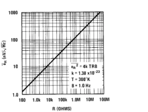
graph is shown inFigure 3 drawn from Figure 2 . To make
this plot, the thermal noise eRof the input resistance must
be calculated from Equation 2 or taken from the graph of Figure 4 . Remember that each term in Equation 3 must be
squared prior to addition, so the data fromFigure 4 and from
Figure 2 is squared. A sample of this calculation follows:
TL/H/7414 – 3
FIGURE 3. Total Noise for the Op Amp ofFigure 2
TL/H/7414 – 4
FIGURE 4. Thermal Noise of Resistor
Example 1: Determine total equivalent input noise per unit bandwidth for an amplifier operating at 1 kHz from a source
resistance of 10 kX. Use the data fromFigures 2 and 4 .
1. Read eRfromFigure 4 at 10 kX; the value is 12.7 nV/0Hz.
2. Read enfromFigure 2 at 1 kHz; the value is 9.5 nV/0Hz.
3. Read infromFigure 2 at 1 kHz; the value is 0.68 pA/0Hz.
Multiply by 10 kXto obtain 6.8 nV/0Hz.
4. Square each term individually, and enter into Equation 3.
eNe
0
en2aeR2ain2Rgen2 e0
9.52a122a6.82 e0
279 eNe17.4 nV/0HzThis is total rms noise at the input in one Hertz bandwidth at 1 kHz. If total noise in a given bandwidth is desired, one must integrate the noise over a bandwidth as specified. This is most easily done in a noise measurement set-up, but may be approximated as follows:
1. If the frequency range of interest is in the flat band; i.e.,
between 1 kHz and 10 kHz inFigure 2 , it is simply a
matter of multiplying eNby the square root of the
band-width. Then, in the 1 kHz – 10 kHz band, total noise is
eNe17.409000
e1.65mV
2. If the frequency band of interest is not in the flat band of Figure 2 , one must break the band into sections, calculat-ing average noise in each section, squarcalculat-ing, multiplycalculat-ing by section bandwidth, summing all sections, and finally taking square root of the sum as follows:
eNe
0
eR2Ba& i 1 (en2ai n2Rgen2)iBi (5)where: i is the total number of sub-blocks.
For most purposes a sub-block may be one or two octaves. Example 2 details such a calculation.
Example 2: Determine the rms noise level in the frequency
band 50 Hz to 10 kHz for the amplifier ofFigure 2 operating
from Rgene2k.
1. Read eRfromFigure 4 at 2k, square the value, and
multi-ply by the entire bandwidth. Easiest way is to construct a table as shown on the next page.
2. Read the median value of enin a relatively small
frequen-cy band, say 50 Hz – 100 Hz, fromFigure 2 , square it and
3. Read the median value of inin the 50 Hz – 100 Hz band
fromFigure 2 , multiply by Rgene2k, square the result
and enter in the table.
4. Sum the squared results from steps 2 and 3, multiply the
sum byDfe100 – 50e50 Hz, and enter in the table.
5. Repeat steps 2 – 4 for band sections of 100 Hz – 300 Hz, 300 Hz – 1000 Hz and 1 kHz – 10 kHz. Enter results in the table.
6. Sum all entires in the last column, and finally take the square root of this sum for the total rms noise in the 50 Hz – 10,000 Hz band.
7. Total enis 1.62mV in the 50 Hz – 10,000 Hz band.
CALCULATING S/N and NF
Signal-to-noise ratio can be easily calculated from known signal levels once total rms noise in the band is determined. Example 3 shows this rather simple calculation from Equa-tion 6 for the data of Example 2.
S/Ne20 log
esig
eN (6)
Example 3: Determine S/N for an rms esige4 mV at the
input to the amplifier operated in Example 2.
1. RMS signal is esige4 mV
2. RMS noise from Example 2 is 1.62mV
3. Calculate S/N from Equation 6
S/Ne20 log 4 mV 1.62mV e20 log (2.47 x 10³) e20 (log 103alog 2.47) e20 (3a0.393) S/Ne68 dB
It is also possible to plot NF vs frequency at various Rgenfor
any given plot of enand in. However there is no specific
all-purpose conversion plot relating NF, en, in, Rgenand f. If
either enor inis neglected, a reference chart can be
con-structed.Figure 5 is such a plot when only enis considered.
It is useful for most op amps when Rgenis less than about
200Xand for FETs at any Rgen(because there is no
signifi-cant in for FETs), however actual NF for op amps with
Rgen l200Xis higher than indicated on the chart. The
graph ofFigure 5 can be used to find spot NF if enand Rgen
are known, or to find enif NF and Rgenare known. It can
also be used to find max Rgenallowed for a given max NF
when enis known. In any case, values are only valid if in
is negligible and at the specific frequency of interest for NF
and en, and for 1 Hz bandwidth. If bandwidth increases, the
plot is valid so long as enis multiplied by0B.
TL/H/7414 – 5
FIGURE 5. Spot NF vs Rgenwhen ConsideringOnly en
and eR(not valid when inRgenis significant)
THE NOISE FIGURE MYTH
Noise figure is easy to calculate because the signal level
need not be specified (note that esigdrops out of Equation
4). Because NF is so easy to handle in calculations, many designers tend to lose sight of the fact that signal-to-noise
ratio (S/N)outis what is important in the final analysis, be it
an audio, video, or digital data system. One can, in fact,
choose a high Rgento reduce NF to near zero if inis very
small. In this case eRis the major source of noise,
over-shadowing encompletely. The result is very low NF, but
very low S/N as well because of very high noise. Don’t be
fooled into believing that low NF means low noiseper se !
Another term is worth considering, that is optimum source
resistance ROPT. This is a value of Rgenwhich produces the
lowest NF in a given system. It is calculated as
ROPTeen
in
(7) This has been arrived at by differentiating Equation 4 with
respect to Rgenand equating it to zero (see Appendix).Note
that this does not mean lowest noise .
For example, usingFigure 2 to calculate ROPTat say 600
Hz,
ROPTe10 nV
0.7 pA
e14 kX
TABLE I. Noise Calculations for Example 2 B (Hz) Df (Hz) en2(nV/Hz) ai n2Rgen2 SUM xDf e (nV2) 50 – 100 50 (20)2e400 (8.7 x 2.0k)2 e 302 702*x 50 35,000 100 – 300 200 (13)2e169 (8 x 2.0k)2 e 256 425 x 200 85,000 300 – 1000 700 (10)2e100 (7 x 2.0k)2 e 196 296 x 700 207,000 1.0k – 10k 9000 (9)2e81 (6 x 2.0k)2 e 144 225 x 9000 2,020,000 50 – 10,000 9950 eR2e(5.3)2e28 28 x 9950 279,000 Total eNe02,626,000e1620 nVe1.62mV
*The units are as follows: (20 nV/0Hz)2e400 (nV)2/Hz (8.7 pA/0Hz x 2.0 kX)2e(17.4 nA/0Hz)2e302 (nV)2/Hz Sume702 (nV)2/Hz x 50 Hze35,000 (nV)2
Then note inFigure 3 , that eNis in the neighborhood of
20 nV/0Hz for Rgen of 14k, while eN e 10 nV/0Hz for
Rgene0 – 100X. STOP! Do not pass GO. Do not be fooled.
Using RgeneR
OPTdoes not guarantee lowest noise
UN-LESS esig2ekR
genas in the case of transformer coupling.
When esig2lkR
gen, as is the case where signal level is
proportional to Rgen(esigekR
gen), it makes sense to use
the highest practical value of Rgen. When esig2kkR
gen, it
makes sense to use a value of RgenkR
OPT. These
conclu-sions are verified in the Appendix.
This all means that it does not make sense to tamper with
the Rgenof existing signal sources in an attempt to make
RgeneR
OPT. Especially, do not add series resistance to a
source for this purpose. It does make sense to adjust Rgen
in transformer coupled circuits by manipulating turns ratio or
to design Rgenof a magnetic pick-up to operate with
pre-amps where ROPTis known. It does make sense to increase
the design resistance of signal sources to match or exceed
ROPTso long as the signal voltage increases with Rgenin at
least the ratio esig2*Rgen. It does not necessarily make
sense to select an amplifier with ROPTto match Rgen
be-cause one amplifier operating at RgeneR
OPTmay produce
lower S/N than another (quieter) amplifier operating with
RgeniR
OPT.
With some amplifiers it is possible to adjust ROPTover a
limited range by adjusting the first stage operating current (the National LM121 and LM381 for example). With these,
one might increase operating current, varying ROPT, to find
a condition of minimum S/N. Increasing input stage current
decreases ROPTas enis decreased and inis simultaneously
increased.
Let us consider one additional case of a fairly complex na-ture just as a practical example which will point up some factors often overlooked.
Example 4: Determine the S/Napparent to the ear of the
amplifier ofFigure 2 operating over 50-12,800 Hz when
driv-en by a phonograph cartridge exhibiting Rgen e1350X,
Lgene0.5H, and average esige4.0 mVrms. The cartridge
is to be loaded by 47k as inFigure 6 . This is equivalent to
using a Shure V15, Type 3 for average level recorded mu-sic.
1. Choose sectional bandwidths of 1 octave each, these are listed in the following table.
2. Read enfromFigure 2 as average for each octave and
enter in the table.
3. Read infromFigure 2 as average for each octave and
enter in the table.
4. Read eRfor the Rgene1350XfromFigure 4 and enter
in the table.
5. Determine the values of Zgenat the midpoint of each
octave and enter in the table.
6. Determine the amount of eRwhich reaches the amplifier
input; this is
eR
R1
R1aZgen
7. Read the noise contribution e47kof R1e47k from
Fig-ure 4 .
8. Determine the amount of e47Kwhich reaches the
amplifi-er input; this is e47k
Zgen
R1aZgen
TL/H/7414 – 7
FIGURE 7. Relative Gain for RIAA, ASA Weighting A, and H-F Boost Curves
TL/H/7414 – 6
9. Determine the effective noise contributed by inflowing
through the parallel combination of R1 and Zgen. This is
in
ZgenR1
ZgenaR1
10. Square all noise voltage values resulting from steps 2, 6, 8 and 9; and sum the squares.
11. Determine the relative gain at the midpoint of each
oc-tave from the RIAA playback response curve ofFigure
7 .
12. Determine the relative gain at these same midpoints
from the A weighted response curve ofFigure 7 for
sound level meters (this roughly accounts for variations in human hearing).
13. Assume a tone control high frequency boost of 10 dB at
10 kHz fromFigure 7 . Again determine relative response
of octave midpoints.
14. Multiply all relative gain values of steps 11-13 and square the result.
15. Multiply the sum of the squared values from step 10 by the resultant relative gain of step 14 and by the band-width in each octave.
16. Sum all the values resultant from step 15, and find the square root of the sum. This is the total audible rms noise apparent in the band.
17. Divide esig e4 mV by the total noise to find S/Ne
69.4 dB.
STEPS FOR EXAMPLE
1 Frequency Band (Hz) 50 – 100 100 – 200 200 – 400 400 – 800 800 – 1600 1.6 – 3.2k 3.2 – 6.4k 6.4 – 12.8k Bandwidth, B (Hz) 50 100 200 400 800 1600 3200 6400 Bandcenter, f (Hz) 75 150 300 600 1200 2400 4800 9600 5 Zgenat f (X) 1355 1425 1665 2400 4220 8100 16k 32k ZgenR1 (X) 1300 1360 1600 2270 3900 6900 11.9k 19k Zgen/R1aZ gen) 0.028 0.030 0.034 0.485 0.082 0.145 0.255 0.400 R1/(R1aZgen) 0.97 0.97 0.97 0.95 0.92 0.86 0.74 0.60
11 RIAA Gain, ARIAA 5.6 3.1 2.0 1.4 1 0.7 0.45 0.316
12 Corr for Hearing, AA 0.08 0.18 0.45 0.80 1 1.26 1 0.5
13 H-F Boost, Aboost 1 1 1 1 1.12 1.46 2.3 3.1 14 Product of Gains, A 0.45 0.55 0.9 1.12 1.12 1.28 1.03 0.49 A2 0.204 0.304 0.81 1.26 1.26 1.65 1.06 0.241 4 eR(nV/0Hz) 4.74 4.74 4.74 4.74 4.74 4.74 4.74 4.74 7 e47k(nV/0Hz) 29 29 29 29 29 29 29 29 3 in(pA/0Hz) 0.85 0.80 0.77 0.72 0.65 0.62 0.60 0.60 2 en(nV/0Hz) 19 14 11 10 9.5 9 9 9 9 e1ei n(ZgenR1) 1.1 1.09 1.23 1.63 2.55 4.3 7.1 11.4 6 e2ee RR1/(R1aZ gen) 4.35 4.35 4.35 4.25 4.15 3.86 3.33 2.7 8 e3ee 47kZgen/(R1aZ gen) 0.81 0.87 0.98 1.4 2.4 4.2 7.4 11.6 10 en2 360 195 121 100 90 81 81 81 e12(from in) 1.21 1.2 1.5 2.65 6.5 18.5 50 150 e22(from eR) 19 19 19 18 17 15 11 7.2 e32(from e47k) 0.65 0.76 0.96 2 5.8 18 55 135 Ren2(nV2/Hz) 381 216 142 122 120 133 147 373 15 BA2(Hz) 10.2 30.4 162 504 1010 2640 3400 1550 BA2Re2(nV2) 3880 6550 23000 61500 121000 350000 670000 580000 16 R(eni2ae 1i2ae 2i2ae 3i2) BiAi2e1,815,930 nV2 eNe0Re1.337mV 17 S/Ne20 log (4.0 mV/1.337mV)e69.4 dB
Note the significant contributions of inand the 47k resistor,
especially at high frequencies. Note also that there will be a difference between calculated noise and that noise mea-sured on broadband meters because of the A curve em-ployed in the example. If it were not for the A curve
attenua-tion at low frequencies, the enwould add a very important
contribution below 200 Hz. This would be due to the RIAA
boost at low frequency. As it stands, 97% of the 1.35mV
would occur in the 800 – 12.8 kHz band alone, principally because of the high frequency boost and the A measure-ment curve. If the measuremeasure-ment were made without either
the high frequency boost or the A curve, the enwould be
1.25mV. In this case, 76% of the total noise would arise in
the 50 Hz – 400 Hz band alone. If the A curve were used, but
the high-frequency boost were deleted, en would be
0.91mV; and 94% would arise in the 800 – 12,800 Hz band
alone.
The three different methods of measuring would only
pro-duce a difference ofa3.5 dB in overall S/N, however the
prime sources of the largest part of the noise and the fre-quency character of the noise can vary greatly with the test or measurement conditions. It is, then, quite important to know the method of measurement in order to know which
individual noise sources inFigure 6 must be reduced in
or-der to significantly improve S/N.
CONCLUSIONS
The main points in selecting low noise preamplifiers are:
1. Don’t pad the signal source; live with the existing Rgen.
2. Select on the basis of low values of enand especially inif
Rgenis over about a thousandX.
3. Don’t select on the basis of NF or ROPTin most cases.
NF specs are all right so long as you know precisely how to use them and so long as they are valid over the
fre-quency band for the Rgenor Zgenwith which you must
work.
4. Be sure to (root) sum all the noise sources en, inand eR
in your system over appropriate bandwidth.
5. The higher frequencies are often the most important un-less there is low frequency boost or high frequency atten-uation in the system.
6. Don’t forget the filtering effect of the human ear in audio systems. Know the eventual frequency emphasis or filter-ing to be employed. APPENDIX I Derivation of ROPT: NFe10 log eR2ae n2ai n2Rgen2 eR2 10 log
#
1aen2 ai n2Rgen2 eR2J
eNF eR e 0.435 (4 kTRB)2 4 kTRB (2R in2)b(e n2ai n2R2)4 kTB 1a(e n2ai n2R2)/4 kTRB where: ReR genSet thise0, and
4 kTRB(2R in2)e4 kTB (e n2ai n2R2) 2 in2R2ee n2ai n2R2 in2R2ee n2 R2ee n2/in2 ROPTeen in APPENDIX II
Selecting Rgenfor highest S/N.
S/Ne
esig2
B(eR2ae
n2ai n2R2)
For S/N to increase with R,
eS/N eR l0 eS/N eR e 2esig(eesig/eR) (eR2ae n2ai n2R2)be sig2(4 kTa2 i n2R) B(eR2ae n2ai n2R2)2
APPENDIX II(Continued) If we setl0, then 2 (eesig/eR) (eR2ae n2ai n2R2)le sig(4 kTa2 i n2R) For esigek 10R,eesig/eRe k1 20R (2 k1/20R) (eR2ae n2ai n2R2)lk 10R (4 kTa2 i n2R) eR2ae n2ai n2R2l4 kTRa2 i n2R2 en2li n2R2 Rke n/in
Therefore S/N increases with Rgenso long as RgensR
OPT For esigek 1R,eesig/eRek 1 2 k1(eR2ae n2ai n2R2)lk 1R (4 kTa2 i n2R) 2 eR2a2 e n2a2 i n2R2l4 kTRa2 i n2R2 eR2a2 e n2l0
Then S/N increases with Rgenfor any amplifier.
For any esigkk
10R, an optimum Rgenmay be determined. Take, for example, esigek
1R0.4,eesig/eRe0.4k 1Rb0.6 (0.8 k1/R0.6) (eR2ae n2ai n2R2)lk 1R0.4(4 kTa2 i n2R) 0.8 eR2a0.8 e n2a0.8 i n2R2l4 kTRa2 i n2R2 0.8 en2l0.2 e R2a1.2 i n2R2
Then S/N increases with Rgenuntil
0.25 eR2a1.5 i
n2R2ee n2
Noise
Specs
Confusing?
LIFE SUPPORT POLICY
NATIONAL’S PRODUCTS ARE NOT AUTHORIZED FOR USE AS CRITICAL COMPONENTS IN LIFE SUPPORT DEVICES OR SYSTEMS WITHOUT THE EXPRESS WRITTEN APPROVAL OF THE PRESIDENT OF NATIONAL SEMICONDUCTOR CORPORATION. As used herein:
1. Life support devices or systems are devices or 2. A critical component is any component of a life
systems which, (a) are intended for surgical implant support device or system whose failure to perform can
into the body, or (b) support or sustain life, and whose be reasonably expected to cause the failure of the life
failure to perform, when properly used in accordance support device or system, or to affect its safety or
with instructions for use provided in the labeling, can effectiveness.
be reasonably expected to result in a significant injury to the user.
National Semiconductor National Semiconductor National Semiconductor National Semiconductor
Corporation Europe Hong Kong Ltd. Japan Ltd.
1111 West Bardin Road Fax: (a49) 0-180-530 85 86 13th Floor, Straight Block, Tel: 81-043-299-2309 Arlington, TX 76017 Email: [email protected] Ocean Centre, 5 Canton Rd. Fax: 81-043-299-2408 Tel: 1(800) 272-9959 Deutsch Tel: (a49) 0-180-530 85 85 Tsimshatsui, Kowloon