Design of Silicon Nano-Bars Anti-Reflection Coating to
Enhance Thin Film Solar Cells Efficiency
Mandana Jalalia,b,c, Hamid Nadgarana,*, and Daniel Ernib,c a
Shiraz University, Department of Physics, Faculty of Science, Eram Square, Shiraz 71454, Iran
b
University of Duisburg-Essen, General and Theoretical Electrical Engineering (ATE), Faculty of Engineering, Duisburg 47048, Germany
c
CENIDE — Center for Nanointegration Duisburg-Essen, Duisburg 47048, Germany *
Corresponding Author Email: [email protected]
Received: May. 7, 2016, Revised: Sep. 26, 2016, Accepted: Nov. 3, 2016, Available Online: Aug. 8, 2017 DOI: 10.18869/acadpub.ijop.11.2.79
ABSTRACT— In this paper a novel anti-reflection (AR) coating based on silicon nano-bars is designed and its impact on the performance of crystalline silicon (c-Si) thin-film solar cells is extensively studied. Silicon nano-bars with optimized size and period are embedded on top of the active layer, under a 100nm Si3N4 layer. As a result of the proposed
layer stack, an inhomogeneous intermediate layer with effective refractive index amid the two layers is formed and a graded refractive index AR coating is achieved, which has a substantial effect on broad, omnidirectional reduction of the reflection spectra. To validate our claim, the proposed structure as well as four conventional AR coatings are simulated and through the numerical analysis of both the spectral response of the reflection factor and the silicon active layer absorption spectra, it is shown that the proposed design outperforms conventional already existing AR coatings, and in addition provides a strong coupling of the incident light to the active layer, while improving the overall efficiency of the thin-film solar cell.
KEYWORDS: Anti-reflection coating, graded refractive index, light coupling, optical absorption, solar cell.
I.
I
NTRODUCTIONThin-film solar cells, due to their substantially reduced active layer thickness, have great potential in solving the energy crisis the world
faces today and hence attracted a great deal of attentions among researchers [1], [2].
However, such thin active layer would have low optical absorption and accordingly poor efficiency due to the limited absorber thickness. To solve this issue, various photon management techniques have been proposed to effectively trap light inside thin-film solar cell active layers [3], [4]. One fruitful technique, which is used in most of solar cells topologies, is based on the inclusion of anti-reflection (AR) coatings that through raising the amount of light input into the active layer, enhances the photon absorption probability [5]-[7]. As AR coatings have various applications, many research have already been conducted leading to several designs as proposed e.g. in [8]-[11]. However, as the solar cell design becomes complicated due to the consideration of the broad solar spectrum, which is represented by the wavelength range from 350nm to 1100nm along the various solar illumination angles during a day, a practical design of efficient AR coatings is certainly subject to further detailed analysis. In this paper we therefore propose a novel design of an omnidirectional broadband AR coating based on c-Si nano-bars covered with a layer of Si3N4. The structure showed a promising
reduction of the reflection spectra even at a 45°
illumination angle. Moreover, strong light coupling to the active layer has been observed as a consequence of the embedded c-Si nanostructure yielding significantly improved solar cell efficiency. To validate performance of the proposed layer design, reflection spectra under various illumination angles are numerically analyzed and further compared with other anti-reflection designs, in conjunction with the corresponding spectral response of the absorption in the thin-film active layer.
Table 1. Anti-reflection coating structures
Structure 1
st
layer (nm)
2nd layer (nm)
3rd layer (nm)
4th layer (nm) A SiO2 (75) MgF2 (60)
B SiO2 (10) Si3N4 (55)
C Al2O3 (205) Si3N4 (22) ZnS (29)
D Al2O3 (21) Si3N4 (14) TaaO5 (18) ZnS (26)
The proposed structure
c-Si Bars, width, w=160 (nm), height, h=45 (nm), period of the grating, ,p=400 (nm)
The first structure (termed as A structure) consists of two layers made of silica and magnesium fluoride, the second (B structure) has two layers of silica and silicon nitride, the third (C structure) contains three layers introducing aluminum oxide, silicon nitride and zinc sulfide, whilst the forth (D structure) encompasses four layers with aluminum oxide, silicon nitride, tantalum pentoxide and zinc sulfide, respectively. In contrast our proposed design introduces a grating made of c-Si nano-bars on top of the c-Si active layer covered with a 100nm thin Si3N4 passivation layer. The
parameters of the nano-bars are optimized using a breeding genetic algorithm [12], [13]. The full details of the analyzed structures are presented in Table 1.
II.
D
IFFERENT ANTI-
REFLECTION STRUCTURESConventional AR coatings consist of different thin, typically quarter-wavelength thick transparent layers with corresponding refractive indexes that are stacked up to reduce the surface reflection. Based on the material choice and the design method, each of the AR
coatings performs in a specific frequency range and their effectiveness is usually further reduced by the angle of incidence. Accordingly, frequency range and angle of incidence are main objectives in anti-reflection designs [14]. Adding more layers to the AR coating is proven to enable further reduction in the reflection however; it also complicates the structure and it may become hard to find a material with appropriate refractive index, as the layers should have graded refractive index to effectively enhance the transmission. On the other hand, broadband designs based on binary gratings involve a large number of layers. Here we propose the introduction of a thin grating structure made of c-Si nano-bars that is covered with a silicon nitride (Si3N4) layer to
create an overall layer with an adjustable effective refractive index. As the nano-bars with their detailed structures are hardly forming a distinct homogeneous layer, their performance is barely affected by the angle of incidence – given a periodicity that is incommensurable to the incident light’s «projected» wavelength onto the surface. To validate our claim, four of AR coating designs that are most common in solar cell applications, are introduced and numerically analyzed in order to compare their effectiveness against the proposed design according to broadband illumination and different angles of incidence.
Fig. 1 Numerical model of the thin film solar cell with the proposed nano-bar-based anti-reflection coating.
III.
R
ESULTS ANDD
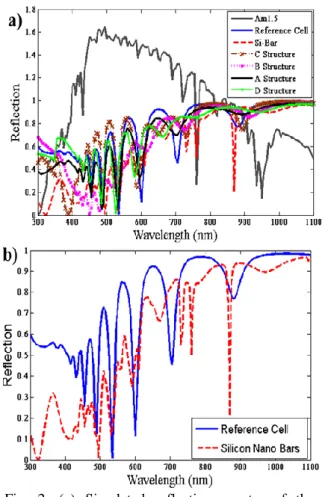
ISCUSSION To study the performance of each structure, a 400nm thick c-Si active layer is considered under which a 40nm Ag layer is embedded as the back-electrode. The AR coatings are deposited on top of the mentioned structure.Fig. 2. (a) Simulated reflection spectra of the structure with (red dashed line) and without (solid blue line) nano-bars versus wavelength. (b) Reflection spectra of all five structures as introduced in Table 1 together with the reference cell and the AM1.5G solar spectrum.
Simulations are carried out for TE plane wave illumination and for angels of incidence encompassing 0°, 15°, 30°, 45°, 60° and 75° relative to the surface normal, yielding a detailed investigation of the surface reflection spectra and the associated spectral response of the active layer’s optical absorption. All numerical investigations rely on the simulation platform COMSOL MultiphysicsTM that is based on the finite element method (FEM). The numerical model of the thin-film soar cell
with the proposed AR coating is illustrated in Fig. 1. The involved c-Si nano-bars have a height of 45nm, and a width of 160nm with a period of 400nm. The grating parameters were optimized using a breeder genetic algorithm where the spectrally integrated optical absorption was maximized as the optimization criteria. The c-Si nano-bars are covered with a 100nm Si3N4 layer, so the bars are fully
embedded in the Si3N4 material leaving a
55nm thick layer of sole Si3N4 on top of the
nano-bars. The result is the formation of two effective layers providing a stepwise grading in the refractive index, which will have a positive impact on the broadband behavior of the reflection reduction.
Table 2. Optical absorption, reflection and carrier generation rate for all the structures introduced in Table 1, as well as a reference cell without any anti-reflection coating.
Structure Optical
absorption Reflection
Carrier generation
rate
A 28.0% 71.7% 16.5%
B 30.0% 69.0% 33.3%
C 22.7% 73.2% -1.5%
D 22.5% 74.1% 4.3%
Si-Bars 37.1% 61.7 48.9% Ref. cell 23.5% 75.6% -
Spectrally integrated reflection and optical absorption as well as the carrier generation rate for all the mentioned structures are provided in the Table 2, which confirms the effectiveness of the proposed structure compared to other AR coatings. Carrier generation rate has been calculated based on the equation 1:
2
1.5 ( )
2
AM E
GR d
(1)Carrier generation rate is weighted according to solar illumination spectrum AM1.5G and hence provides a reliable figure determining the effectiveness of each structure in solar cell designs. The GR figures are illustrated as the relative enhancement compared to the reference cell with no AR coating.
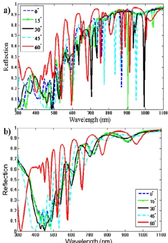
Fig. 3 Simulated reflection spectra in a) c-Si nano-bar structure b) B-structure at various angles of incidence.
A. Reflection spectra
To investigate the effect of c-Si nano-bars on the reflection spectra, the resulting thin-film solar cell is compared in Fig. 2(a) to a bare reference cell without any anti-reflection measures. It has been observed that the reflection is reduced over the whole spectral range, while the reduction is more effective at shorter wavelengths where the solar power spectrum is stronger. At longer wavelengths the reflection reduction is less pronounced leaving room for some transmission resonances.
In Fig. 2(b) the reflection spectra of all five structures are depicted together with the bare reference cell and the AM1.5 solar spectrum. It is clearly shown that the proposed AR coating based on c-Si nano-bars outperforms all other structures. The comparison to the bare reference cell shows that the proposed structure resulted in an 18.4% reduction of the
spectrally integrated reflection. The best performing structure among the four conventional AR coatings is the B-structure, with an overall reflection reduction of 17.1%. The characteristic feature in the other structures is that the reflection reduction is only effective in narrow wavelength ranges while they are barely effective in other regions. This is specially the case for C and D- structures and hence, as presented in Table 2, these structures have very small or no effect on the optical absorption spectra.
One important aspect of the nano-bars is their effectiveness regarding all angles of incidence as they provide an adequate reduction even at 45° illumination angle, while the reflection properties of the four conventional structures visibly degrade at incident angles far from normal. The superiority of the proposed AR coating seems to be tied to the effective layer inhomogeneity caused by the embedded nano-bars. To scrutinize the effectiveness of the proposed design, the resulting reflection spectra are numerically analyzed for various illumination angles (cf. Fig. 3(a)). It is shown that the proposed AR coating works well up to angles around 45° and remains effective even for angles reaching 60°. Reflection spectra for B-structure at same angles is plotted in Fig. 3(b) and from the graph it is conferred that this AR coating is not effective at large illumination angles and beside it is does not impact on the reflection spectra on long wavelength ranges.
B. Absorption spectra
Another interesting feature of the c-Si nano-bars on top of the active layer is an enhanced light in-coupling into the active layer due to the presence of the nano-bars. It is less a distinct grating effect than the creation of hot spots within the active layer, that results in a better optical absorption. As a result of such light in-coupling, each of the grating teeth act as small light source and injects the incident light to the active layer.
Moreover, the grating’s teeth diffusely scatter the incident light inside the active layer and hence the photon path length within the active layer is extended and consequently, photon trapping probability enhances.
Fig. 4 a) Simulated optical absorption spectra of a c-Si thin film solar cell with (red dashed line) and without (solid blue line) c-Si nano-bars anti-reflection coating. b) Simulated optical absorption spectra of a c-Si thin-film solar cell with different AR coatings.
In Fig. 3(a), the optical absorption spectrum of the structure with and without the nano-bars is plotted within the wavelength range from 350nm to 1100nm where the AM1.5G solar spectrum is strong. The absorption spectrum of the bare reference cell is included for comparison showing distinct Fabry-Perot resonances. It is shown that the absorption is improved due to three reasons. First, the active layer volume is slightly increased as the c-Si nano-bars are added to the active layer. Second, the nano-bars spread the incident light diffusely to the active layer and hence an enhanced light in-coupling into the active layer
happens. Third, the inhomogeneity in the effective AR coating layer tends to fill the «gaps» between the Fabry-Perot resonances in the absorption spectrum.
Fig. 5 Simulated electric field distribution at an operating wavelength of a) 530nm, b) 760nm.
The spectrally integrated absorption is enhanced by 57.7% relative to the absorption of the bare reference cell. This enhancement is more pronounced in the wavelength range between350nm-600nm. A possible explanation for such absorption improvement is the emergence of guided modes as well as the strong field localization due to potential resonances in the active layer. Such mechanisms occur virtually at all incident
angles and the numerical analysis show that at an illumination angle of 45° the spectrally integrated optical absorption is further increased to 66.2%. In other AR coating structures such effect is absent and the resulting absorption enhancement is merely due to increased input light. In the Fig. 4(b), simulated optical absorption spectra at normal incident in all the structures are depicted. As concluded from Fig. 4 and Table 2, c-Si-Bars dominantly improved the optical absorption spectra while other structures effect on the optical absorption is merely due to the increased input light within the active layer. To validate our reasoning the electric field distribution within the active layer is analyzed. As shown in the Fig. 5(a), at 530nm each grating tooth acts as a light source and diffusely injects the incident light inside the active layer, while at particular wavelengths such as 760nm (c.f. Fig. 5(b)) light scattering from the teeth creates resonant field localizations that can easily be translated to enhanced optical absorption. The superiority of such peaks in the optical absorption spectra is that they are mostly located in ranges in which solar illumination is strong and correspondingly the carrier generation rate showed a 48.9% enhancement compared to the bare reference cell without any AR coating.
IV.
C
ONCLUSIONIn this paper c-Si nano-bars covered with a layer of Si3N4 forming an inhomogeneous
effective anti-reflection coating is proposed. Due to its simplicity and compactness this approach is especially suitable for thin-film solar cells. The overall structure is thoroughly evaluated through extensive numerical analysis of the top back reflection spectra and the active layer absorption spectra for a solar illumination at various angles of incidence. It is shown that the silicon nano-bars outperform the conventional AR coating designs and are superior with respect to the reflection’s achieved omnidirectionality and its large bandwidth. This is mainly a result of the
effective grading provided by the c-Si nano-bars together with a light spreading effect due to residual scattering yielding an absorption enhancement that is effective up to an angle of incidence of 60°. The spectrally integrated optical absorption for normal incidence is therefore enhanced up to 57.7% relative to the bare reference cell, rendering the proposed AR coating a very compact and versatile solution to the broadband in-coupling problem.
R
EFERENCES[1] H.A. Atwater and A. Polman, “Plasmonic for improved photovoltaic devices,” Nat. Mater., Vol. 9, pp. 205-213, 2010.
[2] F. Hallermann, C. Rockstuhl, S. Fahr, G. Seifert, S. Wackerow, H. Graener, G.V. Plessen, and F. Lederer, “On the use of localized polaritons in solar cells,” phys. stat. sol. (a), Vol. 205, pp. 2844-2861, 2008. [3] K. Nakayama, K. Tanabe, and H.A. Atwater,
“Plasmonic nanoparticle enhanced light absorption in GaAs solar cell,” Appl. Phys. Lett., Vol. 93, pp. 121904, 2010.
[4] M. Jalali and H. Nadgaran, “Photon management of silicon photovoltaics through scattering and near field effect of nanoparticles,” in Proc. 5th international conference on nanostructures(ICNS5), Kish Island, Iran, 2014.
[5] S.J. Oh, S. Chhajed, D.J. Poxson, J. Cho, E.F. Schubert, S.J. Tark, D. Kim, and J.K. Kim, “Enhanced broadband and omni-directional performance of polycrystalline Si solar cells by using discrete multilayer antireflection coatings,” Opt. Exp. Vol. 93, pp. A157-A166, 2013.
[6] R.R. Bilyalov, L. Stalmans, L. Schirone, and C. Lévy-Clément, “Use of porous silicon antireflection coating in multicrystalline silicon solar cell processing,” IEEE Trans. Electron. Devices, Vol. 46, pp. 2035-2040, 1999.
[7] Y.J. Lee, D.S. Ruby, D.W. Peters, B.B. McKenzie, and J.W. Hsu, “ZnO nanostructures as efficient antireflection layers in solar cells,” Nano Lett. Vol. 8, pp. 1501-1505, 2008.
[8] D. Bouhafs, A. Moussi, A. Chikouche, and J. M. Ruiz, “Design and simulation of antireflection coating systems for optoelectronic devices: Application to silicon solar cells,” Solar Energy Mater. Solar Cells., Vol. 59, pp. 79-93, 1998.
[9] K. Bikash, T.B. Pandian, E. Sreekiran, and S. Narayanan, “Benefit of dual layer silicon nitride anti-reflection coating,” Thirty-first IEEE Photovoltaic Specialists Conference., pp. 1205-1207, 2005.
[10]M.F. Schubert, F.W. Mont, S. Chhajed, D.J. Poxson, J.K. Kim, and E.F. Schubert, “Design of multilayer antireflection coatings made from co-sputtered and low-refractive-index materials by genetic algorithm,” Opt. Exp. Vol. 16, pp.5290-5298, 2008.
[11]H. Poor, An Introduction to Signal Detection and Estimation, New York: Springer-Verlag, Ch. 4, 1985.
[12]M. Jalali, H. Nadgaran, and D. Erni, "Semiperiodicity versus periodicity for ultrabroad-band optical absorption in thin-film solar cells," J. Nanophoton. Vol. 10, pp. 036018-036018, 2016.
[13]M. Jalali. H. Nadgaran, and D. Erni, “Implementing Double Grating as a Photon Management Technique in Thin Film Solar Cells,” unpublished.
[14]P. Spinelli, M. A. Verschuuren, and A. Polman. "Broadband omnidirectional antireflection coating based on subwavelength surface Mie resonators." Nat. commun. Vol. 3, pp. 629, 2012.
Mandana Jalali was born at 1985 in Shiraz. She received her BS in solid state physics from Shahid Chamran University in 2007 and MS degree in particle physics from Shiraz University in 2010. Her master thesis was focused on light matter interaction with the
subject of “Compution of the Quantum Efficiency and the Decay Rate for an Emitter in the Vicinity of Nanostructures”. She started her PhD from 2011 in optics and laser at Shiraz University in collaboration with University of Duisburg-Essen. She is the author of more 14 conference papers and has four paper manuscripts ready to be submitted and one paper. Her current research interests include light-matter interaction, plasmonics, photovoltaics, photon management computational physics. She is a member of Iran nanotechnology and physics society of Iran.
Hamid Nadgaran was born at 1958 in Iran. He received his PhD from Manchester University with the title “Measurement and analysis of rotational and torsional energy levels of molecules” at 1992. He is now full professor at Shiraz University and has worked there since 1993. He has published more than 60 papers and one book mainly in optics and laser. His current research interests include nanophotonics, plasmonics, optical metamaterials, laser. He is a member of Iran nanotechnology, physics society of Iran and optics and photonics society of Iran.
Daniel Erni is a full professor at the University of Duisburg-Essen, Germany (http://www.ate.uni-due.de/). He received his two diploma degrees in electrical engineering
from HSR Rapperswil and ETH Zurich in 1986 and 1990, respectively, and his PhD degree in laser physics from ETH Zurich in 1996. He has (co-)authored over 300 publications. Current research include optical interconnects, nanophotonics, plasmonics, optical and electromagnetic metamaterials, RF and biomedical engineering, computational electromagnetics, multi-scale multiphysics modeling and numerical structural optimization. He has won many awards among which he is the winner of the International concept competition «ETH World» and has many memberships. He is Member of the Editorial Board of the Journal of
Computational and Theoretical Nanoscience, Swiss Physical Society (SPS), German Physical Society (DPG), Optical Society of America (OSA), Institute of Electrical and Electronics Engineers (IEEE), Schweizerischer Verband für Elektro-, Energie- und Informationstechnik (SEV), Fellow of the Electromagnetics Academy (EM Academy), Applied Computational Electromagnetics Society (ACES), serec –– swiss electromagnetics research and engineering centre, NRW-NanoCluster for Communication Technology, CENIDE –– Center for Nanointegration Duisburg-Essen.