Design of Wideband CPW Fed Slotted Microstrip Patch
Antenna
Romil Kumar
M.Tech. Research Scholar Dept. ECE, CTIEMT, Shahpur
Jalandhar, India
Nancy Gupta
Assistant Professor Dept. ECE, CTIEMT, Shahpur
Jalandhar, India
Gurpreet Kaur
Assistant Professor Dept. ECE, CTIEMT, Shahpur
Jalandhar, India
ABSTRACT
Microstrip Patch antennas are very prevalent these days due to various attractive features possessed by them. Coplanar Waveguide (CPW) fed patch antenna has benefits of compact size, ease of fabrication and integration with other monolithic circuits. Moreover, the proposed design is very simple design fed with CPW feed. The proposed antenna performs dual band (1.5 GHz and 7 GHz) operation with later band being wideband ranging from 5.32 GHz to 8.27 GHz. Thus, acting as directional wideband antenna with total impedance bandwidth of 2.95 GHz (42%). In addition, various geometric parameters of designed antenna have been varied in order to obtain the desired performance. The Proposed antenna has been designed and simulated using 3D finite element based electromagnetic solver HFSS.
Keywords
Microstrip Patch Antennas, Coplanar Waveguide (CPW), Wideband, Return Loss (S11)
1.
INTRODUCTION
The antenna has been influential in exploiting one of humankind’s greatest natural reserves i.e. the electromagnetic spectrum. In some sense the first antenna ages of 1887, when Heinrich Hertz used a flat dipole for a transmitting antenna and a single turn loop for a receiving antenna to test James Clerk Maxwell's hypothesis [1]. There have been continuous technological advances since then to pace up with human progression. This technological development leads us to modern era of wireless devices.
Today’s person is enclosed by variety of wireless devices in his day to day life such as cellular systems, satellite communications, radio and television sets etc. This would not have been possible without the contribution of antennas. But now the trend is more engrossed towards size compaction and mobility. Therefore, today the structure and size of antennas need to be compact. Also, due to recent wireless and radical multifunctional applications, there has been increasing trend towards multiband and broadband antennas. Microstrip patch antennas are huge popular these days owing to various attractive features possessed by them. Some of the features comprise easily built with PCB technology, low profile structure permitting easy integration with thin devices, light weight and small size, supports both linear and circular polarizations, multi-band operation capable, efficient radiation, low fabrication cost in mass production etc. [2]. Microstrip patch antennas radiate predominantly due to the fringing fields between the patch edges and the ground plane. The electric fields extend beyond the outer periphery, known as fringing fields and are responsible for radiation of patch as an antenna [3]. However, narrow bandwidth is one of the key drawbacks of microstrip antennas. Some other hindrances
include incapability to handle high powers, Surface wave excitation, Low gain, Extraneous radiation due to feeds and junctions etc. [4].
Wong et al. presented a new design of a W-shaped ground plane along with coaxial probe-fed patch antenna to augment the antenna gain and obtain wider bandwidth compared to the conventional planar ground plane-patch antenna [5]. Carlota et al. in 2006 utilized L-probe feed in U-slot antenna to escalate the overall bandwidth of thin substrate patch radiator[6]. In 2014, Majid et al. presented a slotted patch antenna with reflector at its back, to provide reconfigurable response up to six different frequency bands in range within 1.7GHz to 3.5GHz [7]. Abdelaal et al. utilized the CST-MW simulator to propose three different compact circular-ring microstrip patch structures in 2014 to create dual and/or triple broadband frequency response resonating within the fourth generation band (4G) [8]. K. K. Prashar (2014) unified C-shaped slots and Inset feed for rectangular micro-strip patch antenna to broaden the bandwidth from 1.171-2.544 GHz [9]. A. Singh et al. (2014) designed a inverted U-slot patch antenna with short stubs and small rectangular aperture in the ground plane, thus providing electromagnetic coupling to obtain wide frequency response throughout the band from 11.08 GHz to 13.25 GHz[10]. M.R. Hashmi et al. (2006) used coplanar waveguide feeding technology with various space-filling monopole antenna structures to get multiband response with high gain and efficiency [11].
This paper is organized as follows: beginning with introduction, brief idea about CPW technology is provided. Then proposed Antenna design fed by CPW technology is discussed along with its analysis for various geometric parameters. Then, results and discussions are provided followed by conclusion and references.
2.
COPLANAR WAVEGUIDE
TECHNOLOGY
[image:1.595.332.527.702.749.2]As attributed from its name, patch radiator and ground plane shares the same plane above the dielectric substrate, opposed to usual convention of microstrip antennas in which patch surface and ground plane are separated by dielectric substrate. The characteristic impedance and the attenuation of the feed line are resolute by the dimensions of the center strip and the gap as well as the dielectric substrate thickness and permittivity. This basic arrangement is known as conventional CPW [12]. Figure 1 shows the elementary CPW fed structure.
3.
ANTENNA DESIGN AND LAYOUT
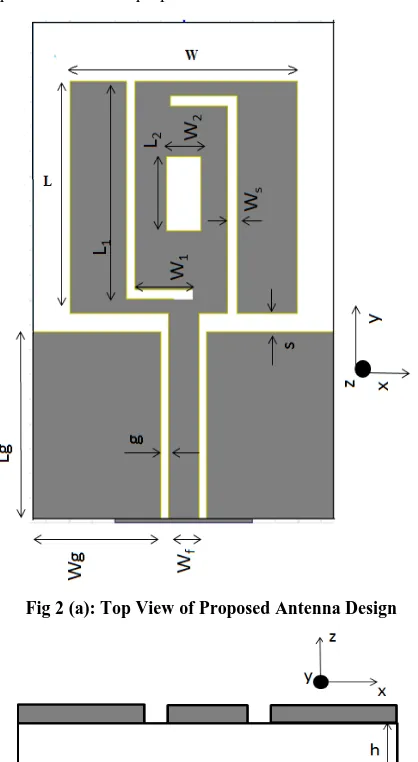
Coplanar waveguide (CPW) fed microstrip patch antenna has been designed using 3D electromagnetic solver HFSS (High frequency structure simulator). Although extended research has been done in this arena already but still lot of geometrical contours are remaining to enhance the bandwidth and other antenna parameters. The designed antenna retains an advantage of compact size, ease of fabrication and integration with other monolithic circuits. Moreover, the proposed design is very simple design fed with CPW feed. The proposed antenna is designed to resonant at two frequencies. The antenna is designed on a FR4 epoxy substrate with dielectric constant ɛr=4.4 and thickness h=1.6mm. Figure 2 shows the
top and side view of proposed antenna structure.
Fig 2 (a): Top View of Proposed Antenna Design
Fig 2 (b): Side View of Proposed Antenna Design
A rectangle radiator is fed by a 50Ω CPW transmission line which is terminated with a sub miniature A (SMA) connector. Wave port is used for excitation in HFSS. The size of port is taken as follows:
Length of the port = 3(2*g+Wf) (1)
Height of the port = 4*h (2)
[image:2.595.324.531.84.453.2]The port height is centralized approximately with respect to CPW metallized area. Table 1 summarizes various geometric parameters of the design.
Table 1: Geometric Parameters of Proposed Design
Parameters Values (mm)
L 18.71
W 19.9
Lg 15
Wg 11.2
g 0.7
s 1.53
Wf 2.6
L1 17.57
W1 5
L2 6
W2 3
Ws 0.8
h 1.6
4.
RESULTS AND DISCUSSIONS
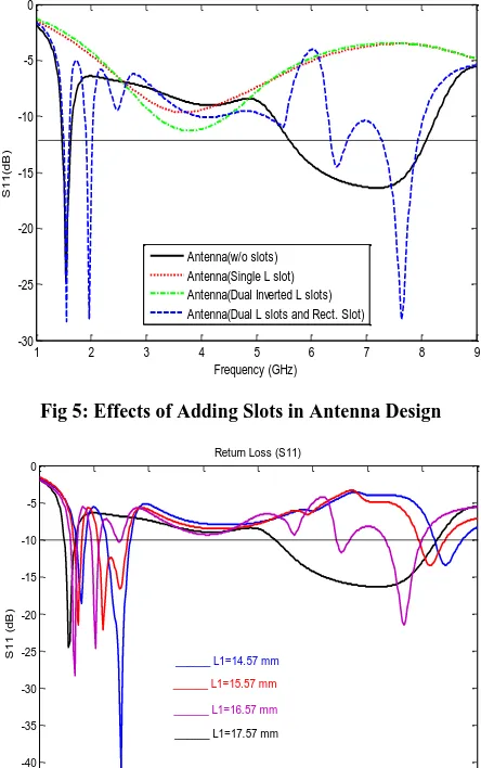
The proposed CPW fed Microstrip patch antenna is analyzed and simulated using Finite Element based HFSS simulator. Figure 3 shows the simulated return loss for the optimized Design with dual inverted L slots and single rectangular slot.
Fig 3: Simulated Return Loss Plot for proposed Design
As it can be seen from Figure 3, the design provides dual band operation at frequencies 1.54 GHz and 7 GHz. The second band results in impedance bandwidth of 2.952 GHz, thus giving wideband operation in second band. The second
1 2 3 4 5 6 7 8 9
-25 -20 -15 -10 -5 0
Frequency (GHz)
S
1
1
(d
B
)
[image:2.595.326.531.88.449.2] [image:2.595.61.270.219.600.2] [image:2.595.319.542.506.678.2]frequency band ranges from 5.32 GHz to 8.27 GHz. The first frequency band results in impedance bandwidth of 0.2 GHz. Group delay explains the rate of change of the total phase shift θ, with respect to the angular frequency ω, as shown below
Group Delay=d(θ)/d(ω) (3)
[image:3.595.319.539.105.288.2]Linear phase throughout the bandwidth indicates constant group delay across the bandwidth. Figure 4 represents the plot of group delay with respect to frequency. It can be seen from figure 4 that except at 1.54 GHz, the group delay is nearly constant throughout the frequency range from 0 to 10 GHz i.e. phase is nearly linear throughout the bandwidth and pulse can be transmitted without much distortion and dissipation. Group delay within tens of nanoseconds is usually acceptable.
Fig 4: Simulated Group Delay of Antenna with Optimal Dimensions
4.1
Effects of Adding Slots in Antenna
Design
Figure 5 shows the effects of adding slots on the return loss parameter of the antenna performance. It can be seen from the fig, that without slots in the patch design, return loss was above -10 dB for the entire frequency range. Thus, initial antenna acting as a poor radiator. When single L slot is added at the patch edge on the positive y axis, return loss is reduced but still not reaching -10 dB criteria. When second inverted L slot is added towards negative y axis edge, return loss is reduced below -10 dB for the frequency range from 6.31 GHz to 8.03 GHz, -28.03 dB at 1.97 GHz and -28.34 dB at 1.55 GHz. Adding rectangular slot at the center of patch radiator results in extensive bandwidth of 2.95 GHz from 5.32 GHz to 8.27 GHz.
4.2
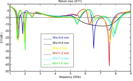
Effects of Changing the Vertical
Length (L1) of Dual Inverted L Slots
Two inverted L shaped slots are introduced in the design of patch radiator. Both slots are having vertical length L1 of 17.57 mm in the optimal design. Effects of changing the vertical length of these slots are analyzed on the performance of antenna using S11 parameter. The resulting plot is shown in Figure 6. Different values of vertical lengths taken are 14.57 mm, 15.57 mm, 16.57 mm and 17.57 mm. Horizontal length W1 is considered as constant in all the four cases and is taken to be 5 mm. It has been analyzed from the graph that return loss is giving optimal performance at L1= 17.57 mm
[image:3.595.317.539.111.465.2]with wider bandwidth. Thus, reducing the height of slots results in deterioration of the antenna performance.
Fig 5: Effects of Adding Slots in Antenna Design
Fig 6: Effects of Changing the Vertical Length (L1) of Dual Inverted L Slots
4.3
Effects of Changing the Horizontal
Length (W1) of Dual Inverted L Slots
The optimum length L1 of L shaped slots has been taken as 17.57 mm based on preceding results. The horizontal lengths of L slots have also been altered to analyze the impact on antenna performance. Different values of W1 have been considered in the range from 3 mm to 7 mm. The S11 parameter for different values of W1 is shown in Figure 7. From the graph, it has been analyzed that horizontal length W1 = 5 mm gives better return loss as compared to other values. Different values of W1 have been taken as 3 mm, 4 mm, 5 mm, 6 mm and 7 mm. It can be inferred from combined plot that W1= 5 mm gives the optimum performance in relatives to others.
4.4
Effects of changing the Width (Ws) of
Dual Inverted L-Shaped Slots
Besides changing the horizontal and vertical lengths (L1 and W1) of L-shaped slots, the width of these slots have also been altered to optimize the performance. Different widths (Ws) of these slots have been taken into consideration such as 0.6 mm, 0.8 mm, 1 mm, 1.2 mm, 1.4 mm and 1.6 mm. The impact of
1 2 3 4 5 6 7 8 9
0 1 2 3 4 5 6 7 8 9x 10
-9 Group Delay
Frequency(GHz)
G
ro
u
p
D
e
la
y
(n
s
)
1 2 3 4 5 6 7 8 9
-30 -25 -20 -15 -10 -5 0
Return Loss(S11)
Frequency (GHz)
S
1
1
(d
B
)
Antenna(w/o slots) Antenna(Single L slot) Antenna(Dual Inverted L slots) Antenna(Dual L slots and Rect. Slot)
1 2 3 4 5 6 7 8 9
-45 -40 -35 -30 -25 -20 -15 -10 -5 0
Return Loss (S11)
Frequency (GHz)
S
1
1
(
d
B
)
[image:3.595.57.275.242.421.2]changing the width of these slots is analyzed by simulating the return loss parameter in HFSS by keeping all other geometric parameters constant. The combined graph is shown in Figure 8.
[image:4.595.57.277.106.434.2]Fig 7: Effects of Changing the Horizontal Length (W1) of Dual Inverted L Slots
Fig 8: Effects of changing the Width (Ws) of Dual Inverted L-Shaped Slots
4.5
Effects of Changing the Length (L2) of
Rectangular Slot
After optimizing lengths (horizontal and vertical) and widths of dual L-shaped slots, the length of single rectangular slot at the centre is also varied to further optimize the performance of antenna. There was not any major choice to vary the width of rectangular slot but still the width of slot is varied between 1 to 3 mm and optimum choice of 3 mm width is taken for rectangular slot. Figure 9 shows the effect of changing the length of rectangular slot from 3 mm to 10 mm at the intervals of 2 mm each. The optimum length (L2) and width (W2) of rectangular slot has come out to be 6 mm and 3 mm respectively.
[image:4.595.61.273.124.253.2]Thus, antenna performance is optimized to get wider bandwidth response by varying different parameters of antenna design as discussed above. The optimized response is shown in figure 3 along with group delay plot in figure 4.
Fig 9: Effects of changing the length (L2) of Rectangular Slot
Radiation pattern is a graphical representation of the radiation properties of the antenna as a function of space coordinates. Figure 10 represents the radiation pattern of antenna at various frequencies. Figure 10(a),10(b), 10(c), 10(d) and 10(e) represents radiation pattern at φ = 0ο
and 90ο at frequencies 1.54 GHz, 5.32 GHz,6.004 GHz, 7.012 GHz and 8.272 GHz. The antenna under test is placed at the origin and is rotated through ɸ= 0° - 360° and θ = 0°-180° to measure the power in the far-field.
Fig 10 (a): Radiation pattern at φ = 0ο and 90ο at 1.54 GHz
Fig 10(b): Radiation pattern at φ = 0ο and 90ο at 5.32 GHz
1 2 3 4 5 6 7 8 9
-35 -30 -25 -20 -15 -10 -5 0
Return Loss (S11)
frequency (GHz)
S
1
1
(d
B
)
______ W1=5 mm
______ W1=3 mm
______ W1=4 mm
______ W1=6 mm
______ W1=7 mm
1 2 3 4 5 6 7 8 9
-50 -45 -40 -35 -30 -25 -20 -15 -10 -5 0
frequency (GHz)
S
1
1
(d
B
)
Return loss (S11)
_____ Ws=0.6 mm
_____ Ws=0.8 mm
_____ Ws= 1 mm
_____ Ws=1.2 mm
_____ Ws=1.4 mm
_____ Ws=1.6 mm
1 2 3 4 5 6 7 8 9
-35 -30 -25 -20 -15 -10 -5 0
Return Loss (S11)
frequency(GHz)
S
1
1
(d
B
)
_____ L2=4mm
_____ L2=6 mm
_____ L2=8 mm
[image:4.595.60.274.291.422.2] [image:4.595.323.536.342.512.2] [image:4.595.322.532.542.720.2]Fig 10(c): Radiation pattern at φ = 0ο and 90ο at 6.004 GHz
Fig 10(d): Radiation pattern at φ = 0ο and 90ο at 7.012
GHz
Fig 10(e): Radiation pattern at φ = 0ο and 90ο at 8.272
GHz
Two values of azimuth angle (φ) has been considered i.e. 0 ο and 90ο to analyze co-polarization and cross-polarization performance. The radiation patterns shown in Figure 10 represents directional radiation pattern i.e. antenna radiates better in some particular directions rather than all directions. Thus, proposed antenna can be used as a directional antenna.
5.
CONCLUSION
Coplanar waveguide fed Microstrip Patch Antenna has been designed using electromagnetic solver HFSS (High frequency
structure simulator). The anticipated antenna resonates at two frequencies. The first frequency being 1.54 GHz having a return loss of -24.5 dB and the second frequency range being from 5.32 GHz to 8.27 GHz, giving total bandwidth of 2.95 GHz, and hence resulting in a wideband antenna. The projected antenna also expresses almost constant group delay throughout the band, thus providing nearly linear phase and undistorted pulse transmission along the band. This antenna provides directional radiation properties suitable for use in Global Positioning Systems (1.5 GHz), Wireless local area networks (5.3 GHz-5.8 GHz), satellite communications for full-time satellite TV networks or raw satellite feeds (C band, 4 GHz-8 GHz) etc. The research work can further be extended to validate the experimental results of the proposed design. Also, the antenna can be analyzed by using defected ground structure in the design.
6.
REFERENCES
[1] Abdelaal, M. & Ghouz, H., 2014. New Compact Circular Ring Microstrip Patch Antennas. Progress In Electromagnetics Research C, 46(January), pp.135–143. [2] Deshmukh,A. A. & Kumar, G., 2005. Compact and
broadband rectangular microstrip antenna using stepped U or V-slot. 2005 IEEE Antennas and Propagation Society International Symposium, 1A, pp.297–300. [3] Kumar, G. & Ray, K., 2003. Broadband microstrip
antennas. Artech House, Antennas and Propagation Library, ISBN 1-58053-244-6.
[4] Lee, K.F. et al., 1996. Experimental Study of a two-element array of U-slot patches. ELECTRONICS LETTERS, 32(5), pp.418–420.
[5] Lopes, F., 2009. Fractal Antennas for Wireless Communication Systems. Integrated Master Thesis,University Do Porto, (June).
[6] Majid, H.A. & Rahim, M.A., 2014. Frequency Reconfigurable Microstrip Patch-Slot Antenna with Directional Radiation Pattern. Progress In Electromagnetics Research, 144(October 2013), pp.319– 328.
[7] Parashar, K., 2014. C-Shaped Slotted Rectangular Microstrip Patch Antenna for Wideband Operation. International Journal of Advanced Electronics and Communication Systems, 3(1), pp.4–6.
[8] Pozar, D.M., 1992. Microstrip antennas. Proceedings of the IEEE, 80(1), pp.79–91.
[9] Salamat, C.D., 2006. L-probe fed multiband microstrip antennas with slots. 2006 Asia-Pacific Microwave Conference, pp.1515–1518.
[10] Singh, A. & Singh, S., 2014. Antenna by Using Inverted U-Slot. International Journal of Antennas and Propagation, Hindawi Publishing Coorporation, 2014(Article ID 306942), pp.1–7.
[11] Singh, S., Agarwal, N., Nitish, N. & Jaiswal, AK., 2012. Design consideration of Microstrip Patch Antenna. International Journal of Electronics and Computer Science Engineering, 2(1), pp.306–316.
[image:5.595.67.271.71.232.2] [image:5.595.61.273.80.428.2] [image:5.595.62.287.376.604.2]