Multilayer Notch Loaded Antenna with Superstrate Layer of 90 deg
Tilted Elements for Wireless Communications
Jai V. Chauhan1, Abhishek Kandwal2, *,
Pornanong Pongpaibool2, and Siwaruk Siwamogsatham2
Abstract—A multilayer notch-loaded antenna for dual-band (L & S) operation has been proposed in this paper for wireless communications. The antenna is multilayered with dielectric layers of FR4 and Rogers/Duroid. A superstrate layer has been introduced with square shaped elements angled at 90 degrees to each other with an empty space just above the patch. The proposed structure of the antenna with superstrate layer is applicable to low frequency consecutive dual-band operations. The antenna also shows very good radiation characteristics with a gain of more than 7.0 dB and side lobe levels reduced to a very good extent of around −20 dB.
1. INTRODUCTION
As technology is progressing, the need for more and more sophisticated communication systems is increased. Communication systems come in a variety of sizes ranging from small hand-held devices to wireless local area networks. The performance of a modern day communication system depends on the characteristics of antenna used. Microstrip technology is not always the first choice for any communication system, but the microstrip antennas have numerous advantages, such as light weight, low volume, planar configuration and easy manufacture. There are also certain challenges associated with microstrip antennas, such as narrow bandwidth, low gain, and low power handling capability [1–3]. From all types of known antennas, dual-band antennas have wide applications in wireless communication systems. Dual-band microstrip antennas have advantage for doubling the system capacity of transmission and reception. Dual-band microstrip antennas may be realized in many ways, such as combining the structures of different sizes [4]. The major drawback of this technique is large size, which makes it difficult to be installed in hand-held terminals. The second method of realizing the dual-band antenna is combining different shapes, such as E-Shape and U-shape [5]. The method used in this paper with different shapes makes the analysis of the antenna a bit tedious. Another method of obtaining a dual-band antenna is by introducing slots [6]. The difficulty with this method is that the radiation characteristics are poor. There are also some other methods, such as L-strip feeding introduction of stub. Dual-polarized suspended square plate rectenna with inserted annular rectangular ring slot has been proposed for low frequencies [7, 8]. Dual-band dual-polarized antennas and compact notch-loaded antennas in frequency bands other than L and S have also been proposed [16–18]. Multi-layering or stacking of antennas increases the overall structure volume, but it is still considered one of the best ways to enhance bandwidth of the antenna. In the present design, a multilayer structure with superstrate is proposed. In most of the present literature, it is clear that it is difficult to obtain dual-band characteristics with good radiation properties in two close dual-bands such as L-S, S-X, especially in the low frequency. The proposed antenna operates in L & S bands and gives good antenna properties, such
Received 5 February 2016, Accepted 21 March 2016, Scheduled 29 March 2016
* Corresponding author: Abhishek Kandwal (kandwal abhishek@rediffmail.com).
1 Tata Institute of Fundamental Research (TIFR), Mumbai, India. 2 RF Electronics Lab, Wireless Information Security &
as wide bandwidth, high gain, and low side lobe level compared to other designs in the same frequency region [19, 20].
In this paper, a novel multilayer notch-loaded disk patch dual-band antenna design with superstrate square-shaped elements tilted at 90 degrees to each other is proposed. The antenna resonates in L and S bands with resonating frequencies 1.725 GHz and 2.4 GHz, respectively. The design consists of a combination of high and low dielectric constant substrates in five layers. The high dielectric constant substrate used is glass epoxy FR4. The low dielectric constant substrate used is Rogers Duroid RT 5880. The patch is in the form of a circular disk with a notch. The antenna is fed by a coaxial probe. The antenna has a good considerable gain at both the resonating frequencies with reduced side-lobe level. The antenna is fabricated by using standard printed circuit board technology (PCBT). All obtained results confirm that the proposed design is a good option for modern day wireless communication systems at low frequency.
2. ANTENNA GEOMETRY
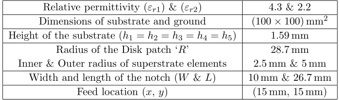
The geometry of the proposed multilayer microstrip antenna is shown in Fig. 1. The top view of the designed antenna shows that the antenna consists of a circular disk patch of radius R with a notch of width W and length L. The side view of the antenna shows a multilayer structure. The substrate comprises five layers of two different dielectric materials. The dielectric materials used are of low and high permittivities. Commercially available FR4 works as dielectric material of high permittivity. Rogers Duroid RT 5880 (loss free) is another dielectric material of low permittivity. There are three layers of Rogers Duroid RT 5880 (loss free) and two layers of FR4. The height and permittivity of FR4 and Roggers Duroid RT 5880 (loss free) are h1, h2 and εr1, εr2, respectively. The superstrate layer (Rogers Duroid) placed at a gap of 1 mm from top of the patch consists of square-shaped elements. The inner and outer radii of each element are 2.5 mm and 5 mm, respectively. All the elements are angled (rotated) at 90 degrees. Design specifications of the antenna are shown in Table 1. All the above shown parameters have been obtained after extensive simulations and using numerical techniques. The radius of the notch loaded circular patch has been chosen using 3D-optimization method and standard equation to calculate the dimensions [3]. The superstrate elements have first been optimized using 3D-solver by considering a single unit cell to obtain resonance and then rotated at an angle of 90 deg to obtain best characteristics. The feed location has been varied at different points, and the dual band is obtained at (15 mm, 15 mm) from the center of the patch.
Table 1. Design specifications.
Relative permittivity (εr1) & (εr2) 4.3 & 2.2 Dimensions of substrate and ground (100×100) mm2 Height of the substrate (h1 =h2 =h3 =h4=h5) 1.59 mm
Radius of the Disk patch ‘R’ 28.7 mm Inner & Outer radius of superstrate elements 2.5 mm & 5 mm
Width and length of the notch (W &L) 10 mm & 26.7 mm Feed location (x,y) (15 mm, 15 mm)
3. ANALYSIS OF MULTILAYER DISK PATCH ANTENNA (WITHOUT SUPERSTRATE)
C1 L1 R1
(a) (b)
(c) (d) (e)
Figure 1. Geometry of the proposed antenna design. (a) Side view. (b) Top view. (c) Equivalent circuit for fed disk patch. (d) Modified equivalent circuit with notch cut in circular disk patch. (e) Geometry with superstrate layer.
inductance (L1) and resistance (R1), and the values of which can be calculated as [2].
C1 = QT 2πR1fr
(1)
L1 = R1
2π frQT (2)
R1 = h 2
1E02jn2(kx0)
2PT (3)
where,Jn(kx0) = Bessel functions of ordern,x0= feed location from the center of the disk patch, h1 = thickness between ground plane and fed patch, QT = total quality factor of the resonator, PT = total
power loss in the cavity, andfr = resonant frequency of the disk antenna for TM11 mode.
But the effective radius of the disk changes, and consequently the resonance frequency also changes. Thus, the resonance frequency of the disk is given by [9–13].
fr= knmc 2πRe√εr1
where, knm = mth zero of the derivative of Bessel function of order n, c = velocity of light, Re =
effective radius of the circular disk [9–13]
Re=
LeWe
π εr1 = effective dielectric constant of the substrate.
In the proposed geometry, the effective dielectric constant for the fed patch is given by [13]
εr1 = εrs + 1
2 +
εrs−1
2
1 + 10h1 R
−1 2
where, h1 is the thickness between ground and fed patch, and
εrs=
n
i=1hi
n
i=1
hi
εri
where, nis the number of stacked layers.
The resonant frequency of the fed patch can be calculated as
f1 = C0 2R√εr1
1−D
1 +Dln
1.123R√εr1 h1
(5)
where, C0= velocity of light in free space
D= 2h1 πBεe1R and
B = h1 R
R h1
+ 1.393 + 0.667 ln
R h1
+ 1.444
where, R is the radius of circular disk patch.
4. ANALYSIS OF NOTCH LOADED MULTILAYER DISK PATCH ANTENNA (WITHOUT SUPERSTRATE)
By cutting a notch from the patch, resonant frequencies of the initial patch changes. The current along the length of the patch remains the same but increases along the width of the patch. This effect is accounted as an additional inductance (ΔL) and additional capacitance (ΔC) in the initial patch. Hence a dual-resonant circuit is obtained. One is an LCR circuit due to initial patch, and the other is due to additional inductance (ΔL) and additional capacitance (ΔC). Fig. 1(d) shows the modified equivalent circuit with notch.
The values of series inductance(ΔL) and series capacitance (ΔC) are calculated by formulae given below,
ΔL= h1μ0π 8 Ls W (6)
where, μ0= 4π×10−7H/m
ΔC =
Ls
W
Cg (7)
where, Ls is the length of notch and W the width of notch,Cg = Gap capacitance which is calculated
by [14].
The total input impedance of the proposed antenna is given as
ZT = 1 1
R1 +
1
jωLT +jωCT
(8)
in which,
LT = L1+ ΔL CT = CC1ΔC
1+ ΔC
5. RADIATION PATTERN
The radiation pattern for the notch-loaded circular disk patch antenna is calculated by considering it as rectangular patch [15]
E(θ) = Jnk0RV0ejk0r1[Jn+1(k0Rsinθ)−Jn−1(k0Rsinθ)]·cosnφ (9) E(φ) = Jnk0RV0e−jk0r1[Jn+1(k0Rsinθ)−Jn−1(k0Rsinθ)]·cosθsinnφ (10) where, V0 = radiating edge voltage, r1 = distance of an arbitrary far-field point, andR= radius of fed disk patch.
6. RESULTS
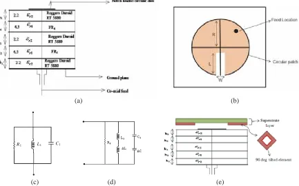
The proposed antenna design is simulated using finite element method (FEM) based simulation software HFSS. After analyzing the theoretical and simulated results, the proposed antenna is fabricated by using standard printed-circuit-board technology (PCBT). After fabricating the prototype shown in Fig. 2, the designed antenna is excited by coaxial probe. The designed prototype is experimentally tested using R & S ZVL Vector network analyzer model no. ZV-Z132. Fig. 3 shows the variation ofS-parameters with frequency for designed prototype. It shows a comparison of theoretical, simulated, measured results at different resonant frequencies and also with superstrate layer. From the graph, it is observed that the antenna resonates in L-band. The simulated resonant frequency is found to be 1.725 GHz in the frequency range 1.686 GHz to 1.776 GHz with return loss 18.31 dB and impedance bandwidth of about 5%. The experimentally measured resonating frequency is also found to be 1.725 GHz in the frequency range 1.690 GHz to 1.770 GHz with a return loss 18.39 dB and impedance bandwidth of about 4.5%.
(a)
(c)
(b)
The introduction of superstrate layer results in improvement of return loss of the antenna. The return loss is improved from 18 dB to 25 dB respectively at the resonant frequencies with almost the same bandwidth.
Figure 3 shows the variation of return loss with frequency in S-band that is in the frequency range from 2–4 GHz. From the graph, it is observed that the simulated resonant frequency is 2.4 GHz in the frequency range 2.341 GHz to 2.462 GHz with return loss 22.21 dB. The impedance bandwidth calculated from this graph is about 5.04%. The experimentally measured resonating frequency is found to be 2.4 GHz in the frequency range 2.35 GHz to 2.469 GHz with return loss 23.21 dB. The impedance bandwidth calculated is about 5%. The return loss with the superstrate layer has been improved from 22 dB to 40 dB which is very good for better transmission. Fig. 3 also shows the theoretical variation (without superstrate layer) of return loss with frequency. From the graph, it is observed that the resonant frequency calculated theoretically is found to be 1.4 GHz in L-band and 2.39 GHz in S-band, respectively.
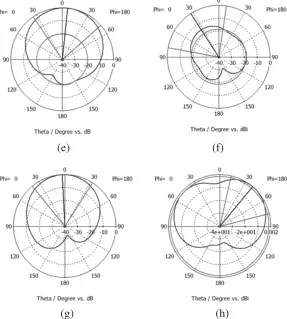
Figure 4 shows the directivity plots of the proposed notch-loaded antenna design with a superstrate layer. Fig. 4(a) shows directivity plot in L-band at frequency 1.725 GHz in polar coordinates. From the graph, it is observed that the main lobe magnitude is about 7.5 dBi with a reduced side-lobe level about
−19.8 dB. Fig. 4(b) shows the directivity of the prototype in S-band at the resonant frequency 2.4 GHz in polar Coordinates. From the graph it is observed that the main lobe magnitude is about 7.6 dBi with
Figure 3. Comparison of simulated, measured and theoretical results in L and S bands.
(a) (b)
a reduced side-lobe level about −21.7 dB. Fig. 5 shows the variation of relative radiative power with angle calculated from LCR equivalent circuit of the prototype at the two resonating frequencies. The complete normalized radiation (power) patterns are shown in Fig. 6. This graph includes the polar plot patterns in yz-plane and xz-plane at two resonant frequencies, i.e., 1.725 GHz and 2.4 GHz.
Therefore, from the obtained results it is clear that the proposed multilayer notch-loaded disk patch antenna shows dual-band characteristics with good radiation characteristics. The antenna resonates in LS band with a good return loss and achieves a reasonable impedance bandwidth. The side-lobe level is also reduced to a very good extent along with a reasonable gain making it a good candidate for antenna applications.
-80 -60 -40 -20 0 20 40 60 80 -18
-16 -14 -12 -10 -8 -6 -4 -2 0
Radiation Pattern
Angle (degree)
Theoretical First center frequency
Theoretical Second Center frequency
Relative Radiative power (dB)
Figure 5. Theoretical variation of relative radiative power with angle at both resonating frequencies.
(a) (b)
(e) (f)
(g) (h)
Figure 6. Normalized radiation patterns in yz-plane and xz-plane at 1.725 GHz and 2.4 GHz. (a) yz-co (1.725 GHz). (b) yz-cross (1.725 GHz). (c) yz-co (2.4 GHz). (d) yz-cross (2.4 GHz). (e) xz-co (1.725 GHz). (f)xz-cross (1.725 GHz). (g)xz-co (2.4 GHz). (h)xz-cross (2.4 GHz).
7. CONCLUSIONS
A novel design of a dual-band notch-loaded disk-patch antenna using multilayer substrates and superstrate layer with square-shaped elements is proposed. The proposed dual-band antenna prototype shows good radiation characteristics at both bands. An impedance bandwidth of 5% in both bands with a gain greater than 7 dB has been obtained. The side-lobe level is reduced to a very good extent of about −20.0 dB. From the obtained results, it is clear that the proposed antenna design achieves good dual-band antenna characteristics. The proposed antenna design meets all the requirements of a dual-band antenna and is a good option for modern communication systems especially for low frequency applications in LS band.
REFERENCES
1. Kumar, G. and K. P. Ray, Broadband Microstrip Antennas, Artech House, Norwood, 2003. 2. Bahl, J. and P. Bhartia, Microstrip Antennas, Artech House Inc., London, 1985.
3. Balanis, C. A., Antenna Theory: Analysis and Design, Wiley, 2005.
5. Abu Tarboush, H. F. and H. S. Al-Raweshidy, “A connected E-shape and U-shape dual-band patch antenna for different wireless applications,” The Second International EURASIP Work-Shop on RFID Technology (EURASIP’08), Budapest, Hungary, 2008.
6. Ghalibafan, J., A. R. Attari, and F. Hojjat-Kashani, “A new dual-band microstrip antenna with U-shaped slot,”Progress In Electromagnetics Research C, Vol. 12, 215–223, 2010.
7. Phongcharoenpanich, C. and K. Boonying, “A 2.4-GHz dual polarized suspended square plate rectenna with inserted annular rectangular ring slot,”Int. J. RF and Microwave Comp. Aid. Eng., 2015, doi: 10.1002/mmce.20949.
8. Chawanonphithak, Y. and C. Phongcharoenpanich, “Miniaturized dual-band II-shaped monopole antennas with modified rectangular ground plane,” 11th International Conference on Electrical Engineering/Electronics, Computer, Telecommunications and Information Technology, 1–4, May 2014.
9. Khairuddin, A. W. and S. H. Al-Charchafchi, “Using equivalent dielectric constant to simplify the analysis of patch microstrip antenna with multilayer substrates,” Antennas and Propagation Society International Symposium, Vol. 2, 676–679, 1998.
10. Zhong, S. and G. Liu, “Improved transmission line model for input impedance of rectangular microstrip antennas with multi-dielectric layers,” Antennas and Propagation Society International Symposium, Vol. 1, 492–495, 1994.
11. Waterhouse, R. B., “Stacked patches using high and low dielectric constant material combinations,”
IEEE Trans. Antennas Propag., Vol. 47, 1767–1771, 1999.
12. Zhong, X.-J., L. Chen, Y. Shi, and X.-W. Shi, “A dual-band single-layer circularly polarized reflectarray composed by elements having variable rotation angles,” Int. J. RF and Microwave Comp. Aid. Eng., Vol. 25, 39–47, 2015, doi: 10.1002/mmce.20821.
13. Shen, L. C., et al., “Resonant frequency of a circular disk printed circuit antenna,” IEEE Trans. Antennas and Propag., Vol. 25, 595–596, 1977.
14. Zhang, X. and F. Yang, “Study of a slit cut on a microstrip antenna and its applications,”Microwave Opt. Technology Letters, Vol. 18, 297–300, 1998.
15. Derneryd, A. G., “Analysis of microstrip disk antenna element,” IEEE Trans. Antennas Propag., Vol. 27, 660–664, 1979.
16. Songa, L. Z. and Y. M. Nieb, “A dual-polarized printed monopole antenna for C-band radar systems,”Journal of Electromagnetic Waves and Applications, Vol. 28, No. 11, 1–8, 2014.
17. Kandwal, A., J. V. Chauhan, and S. K. Khah, “A new compact efficient parasitically coupled notch-loaded antenna,” Vol. 1, 128–133, 2013.
18. Behera, S. and K. J. Vinoy, “Microstrip square ring antenna for dual-band operation,”Progress In Electromagnetics Research, Vol. 93, 41–56, 2009.
19. Liao, W., Q. X. Chu, and S. Du, “Tri-band circularly polarized stacked microstrip antenna for GPS and CNSS applications,”ICMMT Proceedings, 252–255, 2010.