IJSRST184198 | Received : 10 Jan 2018 | Accepted : 25 Jan 2018 | January-February-2018 [ (4) 2: 440-445]
© 2018 IJSRST | Volume 4 | Issue 2 | Print ISSN: 2395-6011 | Online ISSN: 2395-602X Themed Section: Science and Technology
440
A Normal I/O Order Radix-2 FFT Architecture for High Speed Applications
K. Ravi Kumar
PG Scholar, JNTUA College of Engineering, Anantapuramu, Andhra Pradesh, India
ABSTRACT
Nowadays, many applications require simultaneous computation of multiple independent Fast Fourier transform (FFT) operations with their outputs in natural order. Therefore, this paper presents a pipelined Fast Fourier Transform (FFT) processor for the computation of two independent data streams. This architecture is based on the Multipath Delay Commutator (MDC) FFT architecture. It has an N/2-point Decimation In Time (DIT) FFT and an N/2-point Decimation In Frequency (DIF) FFT to process the odd and even samples of two data streams separately. The main feature of this architecture is that the bit reversal operation is performed by the architecture itself, so the outputs are generated in normal order without any dedicated bit reversal circuit. The bit reversal operation is performed by the shift registers in the FFT architecture by scheduling the data. Therefore the proposed architecture take less time and has a high throughput.
Keywords: Fast Fourier Transform (FFT), Decimation in Frequency (DIF) FFT, Decimation in Time (DIT) FFT, Bit reversal, Reorder shift registers (RSR), Multipath Delay Commutator (MDC) FFT, Normal Order.
I.
INTRODUCTION
Fast Fourier Transform (FFT) is one of the frequently used operations in the high speed applications, such as wireless communications, orthogonal frequency division multiple (OFDM) accesses, signal processing applications, digital video broadcasting and also in medical application like electrocardiogram (ECG) etc. The basic radix-2 Fast Fourier Transform plays an important role to computation of the FFT computations. FFT computations we can calculate by using two methods. Those are decimation in frequency (DIF) FFT and decimation in time (DIT). In DIF FFT takes input as in normal order and produces outputs are in bit reversal order. Where as in DIT FFT takes input as in bit reversal order and produces outputs are in normal order.
FFT architectures can be classified into three types of architectures. These are column FFT architecture, parallel FFT architecture and pipeline FFT architecture. In all these pipeline architecture is very attractive in the multimedia communication systems which are FFT processor in their systems. A family of
pipeline FFT architectures are described in [1] in which single path delay feedback (SDF) and multipath delay commutator are popular. There are some applications like image processing, wireless applications, multimedia applications, OFDM and so on, in which more than one independent data streams needs to be processed. Therefore, simultaneous multiple FFT operations are required and also needed separate bit reversal circuit to get the outputs in natural order.
order. These bit reversal circuits are plays an important role to calculate the computation of FFT.
In single delay feedback [7], this is one of the pipeline FFT architecture to compute FFT for a normal I/O order. In this architecture, we are using some processing elements (PE) and delay elements. The stages of the single delay feedback FFT architecture can be divided into based on the N-point FFT computation. For example, to calculate 16-point FFT calculation we can require four stages and delay elements. For this each stage require some processing elements and delay elements. For getting the outputs are in natural order this FFT architecture require separate circuit. In SDF, if we are using FFT as a DIF FFT, the bit reversal circuit is need at the output side and if we are using FFT as a DIT FFT, the bit reversal circuit is used at the input side. This Single path delay feedback FFT architecture takes one input at one clock pulse. To process number of signals through this FFT architecture it takes more time. Hence, this FFT architecture has high latency and low throughput. For this multipath delay commutator (MDC) FFT architecture is proposed.
The proposed FFT architecture is designed to process two independent data streams at a time in less time.
The odd inputs, which are in natural order, are first bit reversed and then processed by N/2-point decimation in time (DIT) FFT. The even samples of the data stream are processed by n/2-point decimation in frequency (DIF) FFT and these even samples are in bit reversal order. The outputs of these both FFT processors are further processed by two parallel butterflies to generate the outputs are in normal order. The bit reversal operation carried out by reorder shift registers and this registers are delay the samples by scheduling the data. As a result this architecture produces the output in less time than prior FFT design.
II.
Proposed pipeline FFT architecture
Fig 1. Idea of the proposed method.
International Journal of Scientific Research in Science and Technology (www.ijsrst.com)
442
The basic idea of computing N-point FFT by using two N/2-point FFT operations with an additional one stage of butterfly operation is as shown in Fig. 1, this is not the exact architecture but provides overview. The reorder blocks shown in figure are reorder the N/2 odd samples (x(2n+1)) are recorded before the N/2 point DIT FFT operation and N/2 even samples (x(2n)) are reordered after the N/2-point DIF FFT operation.In order to compute the N-point DIT FFT from the outputs of two N/2-point FFTs, extra one stage of butterfly operation is performed on the results of the two FFTs. Thus, the outputs generated by additional stage are in normal order.
A. Operation of the proposed FFT architecture:
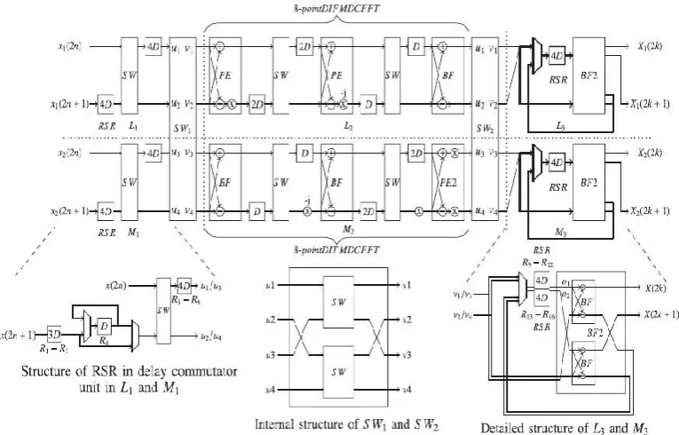
The MDC FFT architecture is in Fig.2. For convenience, the architecture is divided into six levels (L1, L2, L3, M1, M2, and M3). The RSR registers
in the levels L1 and M1 reorder the odd input samples
and the RSR registers in the levels L3 and M3 reorder
the partially processed even data. The 8-point DIF and DIT FFT operations are performed in the levels L2 and M2, respectively. The input data from the level
L1 and M1 can be transferred to the levels L2 and M2
with the help of swapping block SW1. Similarly, the
data from L2 and M2 can be transferred to the levels
L3 and M3, respectively with the help of SW2. SW1
and SW2 have two switches (SW) to swap the data
path and propagate the data to different levels. During the normal mode, these switches pass the data at u1, u2, u3, and u4 to v1, v2, v3, v4 respectively.
During the swap mode, the switches (SW1 and SW2)
pass the data at u1, u2, u3, and u4 to v3, v4, v1 and v2
respectively. SW1 is in the swap mode during the first
N/2 clock cycles and it is in the normal mode during N/2 + 1 to N. On the other hand, SW2 is in the
normal mode during the first N/2 clock cycles and it is in the swap mode during N/2 + 1 to N. Thus, SW1 and SW2are in different modes at any time and change their modes for every N/2 clock cycles.
The two input data streams to the FFT processor are represented as X1 and X2. The odd and even samples
of two input streams are disassociated by the delay commutator units in L1 and M1. X1 is disassociated
into { E1(i, j ), O1(i, j )}, respectively, and X2 is
disassociated into{E2(i, j ), O2(i, j )}. In these
representations, idefines the nature of the data and j defines the number of the data set whose FFT has to be computed. The even set of input data [x(0), x(2), x(4) . . .] is defined as E(1, j )and the odd set of input data [x(1), x(3), x(5) . . .] is defined as O(1, j ). E(2, j )/O(2, j )is the set of scheduled or ordered even/odd data, which are ready to be given to eight-point DIF/DIT FFT. The outputs of eight-point DIF/DIT FFT are defined as E(3, j )/O(3, j ), which are given to the third level for 16-point FFT computation. The table I explains the operation MDC FFT and the data propagation through different levels.
TABLE I
DATA FLOW THROW DIFFERENT LEVELS
1). The first eight samples of X1 are loaded into the
registers (4D in the upper and lower arms of delay commutator unit) in L1. After eight clock cycles, the
switch (SW1) is set in the normal mode and the first
eight samples of X2 are loaded into the registers (4D)
in M1. Simultaneously, E1 (1, 1) (even samples of X1)
is forwarded from L1 to L2 as E1 (2, 1) to perform the
eight-point FFT operation. The odd samples of X1 and
X2 are bit reversed by the RSR in L1 and L2,
respectively. The operation of bit reversing is explained.
2). After eight clock cycles, the positions of the switches SW1 and SW2 are set in the swap mode and
the normal mode, respectively. The odd samples (O1
and the even samples (E2 (1, 1)) of X2 is forwarded
from M1 to L2 as E2 (2, 1). Simultaneously, E1 (2, 1) is
forwarded from L2 to L3 as E1 (3, 1)and reordering is
performed.
3). After eight clock cycles, SW1 and SW2 are set in
the normal mode and the swap mode, respectively. The odd samples of X2(O2(1, 1)) are forwarded from
M1 to M2 as O2(2, 1) and O1(2, 1) is forwarded from
M2 as O1(3, 1) to L3 where the butterfly operations
with E1(3,1) corresponding to the last stage (of the
data stream X1) are performed. In the meantime, E2 (2,
1) from L2 is forwarded to M3 as E2 (3, 1) and
reordering is performed in the RSR.
4).After eight clock cycles, the switch (SW2) is set to
normal position to allow the partially processed odd samples (O2 (3, 1)) from M2 to M3 and perform the
butterfly operations of the last stage (of the data stream X2).
B. Bit Reversing
The proposed architecture having N/2 data scheduled registers before the first butterfly unit are used to separate odd and even samples and delayed them to generate x(n) and x(n + N/2) in parallel. In the proposed architecture, this data scheduling registers are reused to bit reverse odd samples. Similarly, N/2 data scheduling registers are used before the last butterfly unit to store the partially processed even samples until the arrival of odd samples in [7] and here, these registers are reused to bit reverse the partially processed even samples (outputs from DIF FFT). In [5], circuits that use multiplexers and shift registers for bit reversal are proposed. According to [5], if N is the even power of r, then the number of registers required to bit reverse Ndata is (√N - 1 )2 .If
N is odd power of r, then the number of registers are required to bit reverse N data is (√rN - 1)(√N/r - 1),where r is the radix of FFT algorithm. In the proposed architecture, these bit reversal circuits are
incorporated in the data scheduling register to perform to perform the dual role.
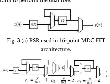
Fig. 3 (a) RSR used in 16-point MDC FFT architecture.
Fig. 3(b) RSR used in N-point MDC FFT architecture.
The RSR used in the 16-point FFT architecture is shown in Fig. 3(a). Actually, this structure is present in the place of shift registers and named as RSR. Generalised RSR for N-point is shown in fig. 3(b) in which c0 is N/4 – (√N/4 -1)2 or N/4-(√(Nr)/4-1)(√N/4r)-1). These registers in c0 do not involve in reordering.
TABLE II
BIT REVERSAL OPERATION IN THE LEVEL L1
TABLE III
International Journal of Scientific Research in Science and Technology (www.ijsrst.com)
444
TABLE IV
BIT REVERSAL OPERATION IN THE LEVEL L3
TABLE V
BIT REVERSAL OPERATION IN THE LEVEL M3
In the proposed FFT architecture, the first N/4 and the next N/4 odd input data to DIF FFT are separately bit reversed as they are required in parallel. Thus, N/4-point bit reversing algorithm is enough and the number of registers required to bit reverse N/4 data is either N/4 – (√N/4 -1)2 or N/4 -(√(Nr)/4-1)(√N/4r)-1)
depending upon the power of two. In Fig. 2, the RSR (R1–R4) in M1 bit reverses the first N/4 odd input data
[x(1), x(3), x(5), and x(7)] and store them in R5–R8
[x(1), x(5), x(3), and x(7)]. After that, the next N/4 odd input data [x(9), x(11), x(13), and x(15)] are bit reversed in R1–R4 [x(9), x(13), x(11), and x(15)],
which is explained in Table II and III. The delay commutator unit in L1 and M1 feeds the bit reversed
odd input samples to u1 and u2, and u3 and u4 (in
SW1), respectively. Similarly, in M3, the RSR (R9–R12)
bit reverses the first N/4 output data [X(0), X(2), X(4), and X(6)] and the RSR (R13–R16) bit reverses the next
N/4 output data [X(8), X(10), X(12), and X(14)] of DIT FFT separately, which is explained in Table IV and V. Thus, the RSR in L3 and M3 bit reverses the
partially processed even data samples from v1 and v2, and v3 andv4 (in SW2), respectively, and feeds to BF2 (via o1 and o2).
III.
SYNTHESIS RESULTS
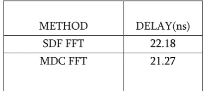
After developing Verilog code for proposed 16-bit MDC FFT Architecture and simulate the developed code in modelsim 6.3f for generating the bits are in normal order. In single path delay feedback to get an output it takes more time when compare to the multipath path delay feedback FFT architecture. MDC FFT architecture can send two data streams with in a less time when comparing with single path delay feedback. So the proposed architecture delay efficient.
From this, proposed architecture decrease the delay 4%, when compare to existing system. Here, the area and power are more than the previous system. But, for high speed applications these two are trade off.
IV.
CONCLUSION
In this paper new approach of Multipath delay commutator (MDC) FFT which are outputs are in normal order and it is used in high speed applications. This FFT architecture is more delay efficient when compared with the previous FFT architectures. This analysis demonstrates that the proposed architecture gives high when it required. Additional work is needed for high order point of FFT architectures such as 32-point,64-point,128-point MDC FFT..etc
.
METHOD DELAY(ns) SDF FFT 22.18
V.
REFERENCES
[1]. S. He and M. Torkelson, "A new approach to
pipeline FFT processor,"in Proc. 10th Int. Parallel Process. Symp., 1996, pp. 766-770.
[2]. Y. Chen, Y.-W. Lin, Y.-C. Tsao, and C.-Y. Lee, " 2.4-Gsample/s DVFS FFT processor for MIMO OFDM communication systems," IEEE J. Solid-State Circuits, vol. 43, no. 5, pp. 1260-1273,May 2008.
[3]. Chu Yu, Member, IEEE, Mao-Hsu Yen, Pao-Ann
Hsiung, Senior Member, IEEE,and Sao-Jie Chen, Senior Member, IEEE," A Low-Power 64-point
Pipeline FFT/IFFT Processor for OFDM
Applications" IEEE Transactions on Consumer Electronics, Vol. 57, No. 1, February 2011.
[4]. K.-J. Yang, S.-H. Tsai, and G. C. H. Chuang, "MDC
FFT/IFFT processor with variable length for MIMO-OFDM systems," IEEE Trans. Very Large Scale Integr. (VLSI) Syst., vol. 21, no. 4, pp. 720-731,Apr. 2013.
[5]. M. Garrido, J. Grajal, and O. Gustafsson, "Optimum
circuits for bit reversal," IEEE Trans. Circuits Syst. II, Exp. Briefs, vol. 58, no. 10, pp. 657-661, Oct. 2011.
[6]. Antony Xavier Glittas, Mathini Sellathurai, and
Gopalakrishnan Lakshminarayanan "A Normal I/O Order Radix-2 FFT Architecture to Process Twin Data Streams "IEEE Transactions On Very Large Scale Integration (Vlsi) Systems, Vol. 24, No. 6, June 2016.
[7]. S.-G. Chen, S.-J. Huang, M. Garrido, and S.-J. Jou, "Continuous-flow parallel bit-reversal circuit for MDF and MDC FFT architectures," IEEE Trans. Circuits Syst. I, Reg. Papers, vol. 61, no. 10, pp. 2869-2877, Oct. 2014.
[8]. M. Garrido, J. Grajal, M. A. Sanchez, and O.