© 2016, IRJET | Impact Factor value: 4.45 | ISO 9001:2008 Certified Journal
| Page 1689
Area–Delay–Power Efficient Carry-Select Adder
Pooja Vasant Tayade
Electronics and Telecommunication, S.N.D COE and Research Centre, Maharashtra, India
---***---Abstract -
In this brief, the logic operations involved in conven-tional carry select adder (CSLA) and binary to excess-1 converter (BEC)-based CSLA are analyzed to study the data dependence and to identify redundant logic operations. We have eliminated all the redundant logic operations present in the conventional CSLA and proposed a new logic formulation for CSLA. In the proposed scheme, the carry select (CS) operation is scheduled before the calculation of final-sum, which is different from the con-ventional approach. Bit patterns of two anticipating carry words (corresponding to cin = 0 and 1) and fixed cin bits are used for logic optimization of CS and generation units. An efficient CSLA design is obtained using optimized logic units. The proposed CSLA design involves significantly less area and delay than the recently proposed BEC-based CSLA. Due to the small carry-output delay, the proposed CSLA design is a good candidate for square-root (SQRT) CSLA. A theoretical estimate shows that the proposed SQRT-CSLA involves nearly 35% less area–delay–product (ADP) than the BEC-based SQRT-CSLA, which is best among the ex-isting SQRT-CSLA designs, on average, for different bit-widths. Carry Select Adder (CSLA) is one of the fastest adders used in many data-processing processors to perform fast arithmetic functions.This work evaluates the performance of the proposed designs in terms of area, power by hand with logical effort and through Xilinx ISE 14.2(Verilog HDL) and this will be implemented in FPGA (Sparton 6).
Key Words
:
Adder, arithmetic unit, low-power design.
1. INTRODUCTION
Low power, area-efficient, and high-performance VLSI systems are increasingly used in portable and mobile devices, multi standard wireless receivers, and biomedical instrumentation [1], [2]. An adder is the main component of an arithmetic unit. A complex digital signal processing (DSP) system involves several adders. An efficient adder design essentially improves the performance of a complex DSP system. A ripple carry adder (RCA) uses a simple design, but carry propagation delay (CPD) is the main concern in this adder. Carry look-ahead and carry select (CS) methods have been suggested to reduce the CPD of adders. A conventional carry select adder (CSLA) is an RCA–RCA configuration that generates a pair of sum words and output-carry bits corresponding the anticipated input-output-carry (cin = 0 and 1) and selects one out of each pair for sum and final-output-carry [3].
A conventional CSLA has less CPD than an RCA, but the design is not attractive since it uses a dual RCA. Few attempts have been made to avoid dual use of RCA in CSLA design. Kim and Kim [4] used one RCA and one add-one circuit instead of two RCAs, where the add-one circuit is implemented using a multiplexer (MUX). He et al. [5] proposed a square-root (SQRT)-CSLA to implement large bit-width adders with less delay. In a SQRT CSLA, CSLAs with increasing size are connected in a cascading structure. The main objective of SQRT-CSLA design is to provide a parallel path for carry propagation that helps to reduce the overall adder delay. Ramkumar and Kittur [6] suggested a binary to BEC-based CSLA.
The BEC- based CSLA involves less logic resources than the conventional CSLA, but it has marginally higher delay. A CSLA based on common Boolean logic (CBL) is also proposed in [7] and [8]. The CBL-based CSLA of [7] involves significantly less logic resource than the conventional CSLA but it has longer CPD, which is almost equal to that of the RCA. To overcome this problem, a SQRT-CSLA based on CBL was proposed in [8]. However, the CBL-based SQRT- CSLA design of [8] requires more logic resource and delay than the largely depends on availability of redundant operations in the formulation, whereas adder delay mainly depends on data dependence. In the existing designs, logic is optimized without giving any consideration to the data dependence.
© 2016, IRJET | Impact Factor value: 4.45 | ISO 9001:2008 Certified Journal
| Page 1690
2. LOGIC FORMULATION
The CSLA has two units: 1) the sum and carry generator unit (SCG) and 2) the sum and carry selection unit [9]. The SCG unit consumes most of the logic resources of CSLA and significantly contributes to the critical path. Different logic designs have been suggested for efficient implementation of the SCG unit. We made a study of the logic designs suggested for the SCG unit of conventional and BEC-based operations and data dependence Accordingly, we remove all redundant logic operations and sequence logic operations
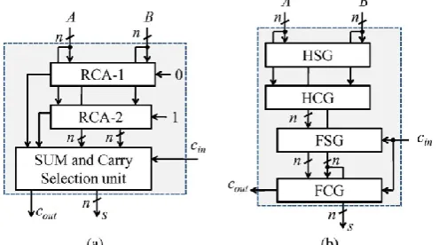
Fig -1: (a) Conventional CSLA; n is the input operand bit-width. (b) The logic operations of the RCA is shown in split form, where HSG, HCG, FSG, and FCG represent half-sum generation, half-carry generation, full-sum generation, and full-carry generation, respectively.
2.1 Logic Expressions of the SCG Unit of the
Conventional CSLA
As shown in Fig. 1(a), the SCG unit of the conventional CSLA [3] is composed of two n-bit RCAs, where n is the adder bit-width. The logic operation of the n-bit RCA is performed in four stages: 1) half-sum generation (HSG); 2) half-carry generation (HCG); 3) full-sum generation (FSG); and 4) full-carry generation (FCG). Suppose two n-bit operands are added in the conventional CSLA, then RCA-1 and RCA-2 generate n-bit sum (s0and s1) and output-carry (c0outand c1out) corresponding to input-carry (cin = 0 and cin = 1), respectively. Logic expressions of RCA-1 and RCA-2 of the SCG unit of the n-bit CSLA are given as
S00(i) = A(i)⊕B(i) C00 (i) = A(i) ·B(i) (1a) S10(i) = S00(i) ⊕ sC0000(i− 1) (1b) C10 (i) = C00 (i) + S00(i) · C10(i− 1) (1c)
S01(i) = A(i) ⊕B(i) C01(i) = A(i) ·B(i) (2a)
S11 (i)= S01 (i)⊕C11(i−1) (2b) C11(i)= C01(i) + S01(i) . C11(i−1) Cout1= C11(n−1) (2C)
Where c01(−1) = 0, c11(−1) = 1, and 0 ≤i ≤ n− 1.
[image:2.595.182.430.187.325.2]© 2016, IRJET | Impact Factor value: 4.45 | ISO 9001:2008 Certified Journal
| Page 1691
Fig -2: Structure of the BEC-based CSLA; n is the input operand bit-width.2.2. Logic Expression of the SCG Unit of the BEC-Based CSLA
As shown in Fig. 2, the RCA calculates n-bit sums01 and c0out corresponding to cin = 0. The BEC unit receives s01 and c0out from the RCA and generates (n + 1)-bit excess-1 code. The most significant bit (MSB) of BEC represents c1out, in which n least significant bits (LSBs) represent s11. The logic expressions of the RCA are the same as those given in (1a)– (1c). The logic expressions of the BEC unit of the n-bit BEC-based CSLA are given as
S1 1
(0) = S1 0
(0) C1 1
(0) = S1 0
(0) (3a)
S1
1(i) =S 0
1(i) ⊕ C 1
1(i − 1) (3b)
C1
1(i) =S 0
1(i) · C 1
1(i − 1) (3c)
C1 out =C0
1
(n − 1) ⊕ C1 1
(n − 1) (3d)
for 1 ≤ i ≤ n − 1.
We can find from (1a)–(1c) and (3a)–(3d) that, in the case of the BEC-based CSLA, c11 depends on S01 , which otherwise has no dependence on S01 in the case of the conventional CSLA. The BEC method therefore increases data dependence in the CSLA. We have considered logic expressions of the conventional CSLA and made a further study on the data dependence to find an optimized logic expression for the CSLA.
[image:3.595.38.554.563.793.2]© 2016, IRJET | Impact Factor value: 4.45 | ISO 9001:2008 Certified Journal
| Page 1692
Fig -3: (a) Proposed CS adder design, where n is the input operand bit-width, and [∗] represents delay (in the unit of inverter delay), n = max (t, 3.5n + 2.7).(b) Gate-level design of the HSG. (c) Gate-level optimized design of (CG0) for input-carry = 0. (d) Gate-level optimized design of (CG1) for input-carry = 1.(e) Gate-level design of the CS unit. (f) Gate-level design of the final-sum generation (FSG) unit.Calculation of s01 is avoided in the SCG unit; 2) the n-bit select unit is required instead of the (n + 1) bit; and 3) small output-carry delay. All these features result in an design for the CSLA. We have removed all the redundant logic operations of (1a)–(1c) and (2a)–(2c) and rearranged logic expressions of (1a)–(1c) and (2a)–(2c) based on their dependence. The proposed logic formulation for the CSLA is given as
s0(i) =A(i) ⊕ B(i) c0(i) = A(i) · B(i) (4a)
C0 1
(i) =C0 1
(i − 1) · s0(i) + c0(i) for (C0 1
(0) = 0) (4b)
C1
1(i) =C 1
1 (i − 1) · s
0(i) + c0(i) for (C11(0) = 1) (4c)
c(i) =C0 1
(i) if (cin = 0) (4d)
c(i) =c11(i) if (cin = 1) (4e)
co ut =c(n − 1) (4f)
s( 0) =s0(0) ⊕ cin s(i) = s0(i) ⊕ c(i − 1). (4g)
3. PROPOSED ADDER DESIGN
The proposed CSLA is based on the logic formulation given in (4a)–(4g), and its structure is shown in Fig. 3(a). It consists of one HSG unit, one FSG unit, one CG unit, and one CS unit. The CG unit is composed of two CGs (CG0 and CG1) corresponding to input-carry ‘0’ and ‘1’. The HSG receives two n-bit operands (A and B) and generate half-sum word s0 and half-input-carry word c0 of width n bits each. Both CG0 and CG1 receive s0 and c0 from the HSG unit and generate two n-bit full-carry words c01 and c11 corresponding to input-carry ‘0’ and ‘1’, respectively. The logic diagram of the HSG unit is shown in Fig. 3(b). The logic circuits of CG0 and CG1 are optimized to take advantage of the fixed input-carry bits. The optimized designs of CG0 and CG1 are shown in Fig. 3(c) and (d), respectively.
The CS unit selects one final carry word from the two carry words available at its input line using the control signal cin. It selects c01 when cin = 0; otherwise, it selects c11. The CS unit can be implemented using an n-bit 2-to-l MUX. However, we find from the truth table of the CS unit that carry words c01 and c11 follow a specific bit pattern. If c01 (i) = ‘1’, then c11 (i) = 1, irrespective of s0(i) and c0(i), for 0 ≤ i ≤ n − 1. This feature is used for logic optimization of the CS unit. The optimized design of the CS unit is shown in Fig. 3(e), which is composed of n AND–OR gates. The final carry word c is obtained from the CS unit. The MSB of c is sent to output as cout, and (n − 1) LSBs are XORed with (n − 1) MSBs of half-sum (s0) in the FSG [shown in Fig. 3(f)] to obtain (n − 1) MSBs of final-sum (s). The LSB of s0 is XORed with cin to obtain the LSB of s.
4. PERFORMANCE COMPARISON
4.1 Area–Delay Estimation Method
We have considered all the gates to be made of 2-input AND, 2-input OR, and inverter (AOI). A 2-input XOR is composed of 2 AND, 1 OR, and 2 NOT gates. The area and delay of the 2-input AND, 2-input OR, and NOT gates (shown in Table 1) are taken from the Synopsys Armenia Educational Department (SAED) 90-nm standard cell library datasheet for theoretical estimation. The area and delay of a design are calculated using the following relations:
Table -1: Area and Delay of AND, OR, and NOT gates given in the saed90-nm standard cell library datasheet
A = a · Na + r · No + i · Ni (5a) T = na · Ta + no · To + ni · Ti (5b)
© 2016, IRJET | Impact Factor value: 4.45 | ISO 9001:2008 Certified Journal
| Page 1693
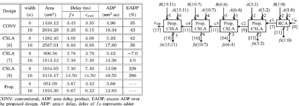
Table -2: General Comparison of Gate Counts and Delay of the Proposed and Existing CSLAS for Single-Stage Design. N: Input Bit-WidthTable -3: Theoretical Estimate of Area and Delay Complexities of The Proposed and Existing CSLAS
Fig -4: Proposed SQRT-CSLA for n = 16. All intermediate and output signals are labeled with delay (shown in square brackets).
the (AND, OR, NOT) gate counts of the total design and its critical path. (a, r, i) and (Ta, To, Ti), respectively, represent the area and delay of one (AND, OR, NOT) gate. We have calculated the (AOI) gate counts of each design for area and delay estimation. Using (5a) and (5b), the area and delay of each design are calculated from the AOI gate counts (Na,No,Ni), (na, no, ni), and the cell details of Table 1.
4.2 Single-Stage CSLA
© 2016, IRJET | Impact Factor value: 4.45 | ISO 9001:2008 Certified Journal
| Page 1694
CSLA, the proposed CSLA involves 0.42 ns more delay, but it involves nearly 28% less ADP due to less area complexity. Interestingly, the proposed CSLA design offers multipath parallel carry propagation, whereas the CBL-based CSLA of [7] offers a single carry propagation path identical to the RCA design. Moreover, the proposed CSLA design has 0.45 ns less output-carry delay than the output-sum delay. This is mainly due to the CS unit that produces output-carry before the FSG calculates the final-sum.4.3 Multistage CSLA (SQRT-CSLA)
The multipath carry propagation feature of the CSLA is
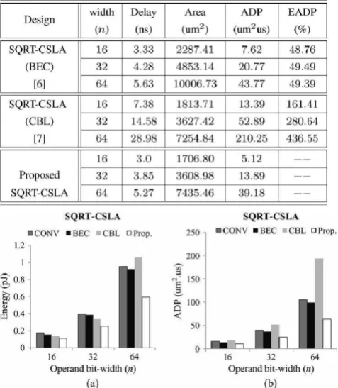
fully exploited in the SQRT-CSLA [5], which is composed of a chain of CSLAs. CSLAs of increasing size are used in the SQRT-CSLA to extract the maximum concurrence in the carry propagation path. Using the SQRT-CSLA design, large-size adders are implemented with significantly less delay than a single-stage CSLA of same size. However, carry propagation delay between the CSLA stages of SQRT-CSLA is critical for the overall adder delay. Due to early generation of output-carry with multipath carry propagation feature, the proposed CSLA design is more favorable than the existing CSLA designs for area–delay efficient implementation of SQRT-CSLA. A 16-bit SQRT-CSLA design using the proposed CSLA is shown in Fig. 4, where the 2-bit RCA, 2-bit CSLA, 3-bit CSLA, 4-bit CSLA, and 5-bit CSLA are used. We have considered the cascaded configuration of (2-bit RCA and 2-, 3-, 4-, 6-, 7-, and 8-bit CSLAs) and (2-bit RCA and 2-, 3-, 4-, 6-, 7-, 8-, 9-, 11-, and 12-bit CSLAs), respectively, for the 32-bit SQRTCSLA and the 64-bit SQRT-CSLA to optimize adder delay. To demonstrate the advantage of the proposed CSLA design in SQRT-CSLA, we have estimated the area and delay of SQRTCSLA using the proposed CSLA design and the BEC-based CSLA of [6] and the CBL-based CSLA of [7] for bit-widths 16, 32, and 64 using Tables I, II, and (5a) and (5b). The estimated values are listed in Table 4. for comparison. As shown in Table 4, the delay of the CBL-based SQRT-CSLA [7] is significantly higher for large bit-widths than the proposed SQRT-CSLA and BEC based SQRT-CSLA designs. Compared with SQRT-CSLA designs of [6] and [7], the proposed SQRTCSLA design, respectively, involves 35% and 72% less ADP, on average, for different bit-widths.
[image:6.595.165.404.421.695.2]
Table -4: Theoretical Estimate of Area and Delay Complexities of The Proposed and Existing SQRT-CSLAS
© 2016, IRJET | Impact Factor value: 4.45 | ISO 9001:2008 Certified Journal
| Page 1695
4.4 Tool Used:
This work evaluates the performance of the proposed designs in terms of area, power by hand with logical effort and through Xilinx ISE 14.2(Verilog HDL).This coding is implemented in FPGA (Sparton 6).The Xilinx 14.2 (Verilog HDL) provide all simulation results. Area, Dealay requirement of all type of carry select adders along with proposed carry select adder, so that its easy to compare and got conclusion that which system is good in all circumstances
4.5 Synthesis Results
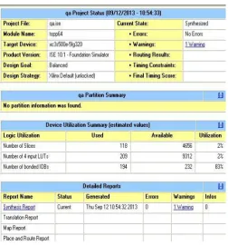
[image:7.595.168.420.327.581.2]We have coded the SQRT-CSLA in VHDL using the pro-posed CSLA design and the existing CSLA designs of [6] and [7] for bit-widths 16, 32, and 64. This work evaluates the performance of the proposed designs in terms of area, power by hand with logical effort and through Xilinx ISE 14.2(Verilog HDL) and this will be implemented in FPGA (Sparton 6). The synthesis result of Table 5. confirms the theoretical estimates given in Table 4. As shown in Table 5, the proposed SQRT-CSLA involves significantly less area and less delay and consumes less power than the existing designs. We can find from Fig. 5 that the proposed SQRT. Table 4. shows CSA 64 bit exist report and table 7. shows CSA 64 bit proposed report which is run on Xilinx ISE 14.2 (Verilog HDL)
© 2016, IRJET | Impact Factor value: 4.45 | ISO 9001:2008 Certified Journal
| Page 1696
Table -6: CSLA 64 Bit Proposed Report5. Evaluation Results
Table -7: Comparison of Regular and Modified Carry Select Adder
As shown in Table 7, the proposed SQRT-CSLA involves significantly less area and less delay and consumes less power than the existing designs which is run on Xilinx ISE 14.2 (Verilog HDL).This will implemented in Sparton 6 kit.
6. CONCLUSION
© 2016, IRJET | Impact Factor value: 4.45 | ISO 9001:2008 Certified Journal
| Page 1697
scheme follow a specific bit pattern, which is used for logic optimization of the CS unit. The proposed CSLA design involves significantly less area and delay than the recently proposed BEC-based CSLA. Due to the small carry-output delay, the proposed CSLA design is a good candidate for the SQRT adder. The ASIC synthesis result shows that the existing BEC-based SQRT-CSLA design involves 48% more ADP and consumes 50% more energy than the proposed SQRT-CSLA, on average, for different bit-widths.REFERENCES
[1] K. K. Parhi, VLSI Digital Signal Processing. New York, NY, USA: Wiley, 1998.
[2] A. P. Chandrakasan, N. Verma, and D. C. Daly, “Ultralow-power electron-ics for biomedical applications,” Annu. Rev. Biomed. Eng., vol. 10, pp. 247– 274, Aug. 2008.
[3] O. J. Bedrij, “Carry-select adder,” IRE Trans. Electron. Comput., vol. EC-11, no. 3, pp. 340–344, Jun. 1962.
[4] Y. Kim and L.-S. Kim, “64-bit carry-select adder with reduced area,” Electron. Lett., vol. 37, no. 10, pp. 614–615, May 2001.
[5] Y. He, C. H. Chang, and J. Gu, “An area-efficient 64-bit square root carry-select adder for low power application,” in Proc. IEEE Int. Symp. CircuitsSyst., 2005, vol. 4, pp. 4082–4085.
[6] B. Ramkumar and H. M. Kittur, “Low-power and area-efficient carry-select adder,” IEEE Trans. Very Large Scale Integr. (VLSI) Syst., vol. 20, no. 2, pp. 371–375, Feb. 2012.
[7] I.-C. Wey, C.-C. Ho, Y.-S. Lin, and C. C. Peng, “An area-efficient carry select adder design by sharing the common Boolean logic term,” in
Proc.IMECS, 2012, pp. 1–4.
[8] S. Manju and V. Sornagopal, “An efficient SQRT architecture of carry select adder design by common Boolean logic,” in Proc. VLSI ICEVENT, 2013, pp.1–5.