Design of an Effective Charge Pump-Phase Locked
Loops Architecture for RF Applications
ABSTRACT
Analog and mixed architectures design with high performance suffered from many difficulties due to low power supply, consumption, and the trend toward reducing the size of the circuit. Currently, these performances are considered one of the main constraints in analog design. Characterized and designed of mixed circuits such as Charge Pump-Phase Locked Loops (CP-PLLs) is a challenge in mixed-signal integrated circuits design. In this paper, an effective CMOS CP-PLLs architecture for RF applications that operates at a low power supply 2V into a large range frequency is presented. The proposed CP-PLLs architecture has two novel design blocks which are respectively Phase Frequency Detector (PFD) and Voltage Controlled Oscillator (VCO). The key advantage of the two novel designs is that uses a simple circuit, provide more stable operation compared with other structures recently used and reduce the chip area overhead. Also, the novel VCO design solved the problems caused by recent structures. The CP-PLLs is designed and evaluated using electrical simulator tolls (ADS) with 0.35μm AMS CMOS technology. Simulations results show a good performance and the effectiveness of the proposed structure.
General Terms
Circuits and Systems.
Keywords
Mixed-Analog Design, CP-PLLs, PFD, VCO, 0.35μm AMS CMOS technology.
1.
INTRODUCTION
Because of a large number of desirable applications, performance parameters and design characteristics CP-PLLs have in recent years become a popular PLL architecture [1-2]. Generally, CP-PLLs are the most common mixed-signal component which is present on the SOCs and digital applications. It is a very pervasive system exploited in diversity applications such as frequency and phase synthesizers, FM and PM demodulators, clock and data recovery systems generate an on-chip clock [2-3] and radio frequency synthesis.
This research focuses on the proposing an effective CP-PLLs architecture for RF applications which has a good performance, less area overhead and low power supply 2V to operate in a large range frequency. In addition, in
the design of CP-PLLs, the novel PFD structure [4] (I.Toihria and al, 2013) has simple circuit and small-size devises, and provides more stable operation while reducing the number of transistors which consists compared with other structures recently used [5-7]. Also, the proposed VCO structure enables to the output signal of the VCO to oscillate between „0‟ and „1‟ for each input value of controlled voltage, varied between 0V to 1.2V, which is difficult to get from the conventional VCO [5].
The outline of this paper is the following. Section 2 presents the basic concept of Charge Pump-Phase Locked Loop. The novel CMOS implementation of PFD and VCO, also all blocks of CP-PLL are presented in section 3. Electrical simulation results with 0.35µm CMOS AMS technology of CP-PLLs are presented in Section 4. Finally, section 5 draws conclusions.
2.
BASIC CONCEPT OF CP-PLLs
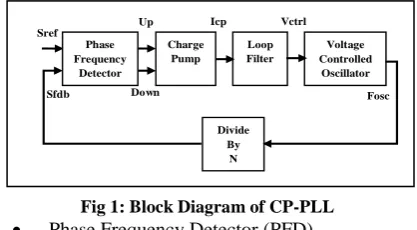
[image:1.595.316.525.526.641.2]The main building components for CP-PLL are: Phase Frequency Detector, Charge Pump, Loop Filter, Voltage Controlled Oscillator and Divide by N. A block diagram of CP-PLLs is shown in Fig.1. For further information on CP-PLLs operation can be found in [1-2-8].
Fig 1: Block Diagram of CP-PLL Phase Frequency Detector (PFD)
PFD is a purely digital system driven by the rising or falling edges of its input signals which are respectively reference signal (𝑆𝑟𝑒𝑓) and feedback signal (𝑆𝑓𝑑𝑏).
Thereafter, the PFD deliver two terminals signal, Up and Down, in the form of three sequential logic states for controlling a 3-state Charge Pump block [2-8-9].
Charge Pump (CP)
Basically, Charge Pump consists of two CMOS switches controlled by the output signals of PFD. It is utilized to convert the sequential logic states of PFD into analog signal [2-8].
Intissar Toihria
University of Sfax National School of Engineering of Sfax Laboratory of Electronic and
Micro-technology Communication (EMC),
Sfax, Tunisia
Rim Ayadi
University of Sfax National School of Engineering of Sfax Laboratory of Electronic and
Micro-technology Communication (EMC),
Sfax, Tunisia
Mohamed Masmoudi
University of Sfax National School of Engineering of Sfax Laboratory of Electronic and
Micro-technology Communication (EMC),
Sfax, Tunisia
Vctrl
Fosc Icp
Down Up
Sfdb Sref
Charge Pump
Loop Filter
Voltage Controlled Oscillator
Divide By N Phase
Loop Filter (LF)
The used LF in the design of CP-PPL is a second order low-pass filter. Its purpose is to convert the charge pump current 𝐼𝑐𝑝 into a voltage controlled signal 𝑉𝑐𝑡𝑟𝑙, to filter
the alternating current component [2-8] and to suppress the noise.
Voltage Controlled Oscillator (VCO)
A VCO block generates an output signal witch this oscillation frequency proportional to the output voltage [2] of Loop Filter.
Divide by N counter (DBN)
The purpose of Divide by N Counter is to divide the oscillation frequency of the output signal provided from VCO by N, 𝐹𝑑𝑖𝑣=𝐹𝑣𝑐𝑜 𝑁, and to generate an feedback signal for every N cycles [10].
3.
DESIGN OF CP-PLLs
3.1
PHASE FREQUENCY DETECTOR
Phase Frequency Detector has been extensively used in the design of Charge Pump-Phase Locked Loops systems of the reasons for their popularity [8-9-12-13]. A new PFD design [4] (I.Toihria and al, 2013) with 0.35µm CMOS technology is shown in Fig.2. The purpose of PFD is to compare the phase lead or the phase lag of its input signals. For example, in the case where it is used in the CP-PLL design, it compares the state of the feedback signal with the reference signal and generates two output signals Up and Down with the pulse width that corresponds to the frequency or phase difference between these compared signals.
[image:2.595.356.481.360.474.2]To assure a proper operation of associated Charge Pump to Phase Frequency Detector, we add an inverter circuit to Up signal and a transmission gate circuit to Down signal. Up and Down terminals of PFD are the input signals of Charge Pump block.
Fig 2: Proposed Structure of PFD (I.Toihria and al)
The proposed PFD structure has simple circuit and small dimension devices, and provide more stable operation with respect to input signal variations while reducing the number of transistor which consists compared with other structures recently used [5-6-13-14]. Furthermore, this circuit has a good performance, less area overhead and assures the same operation compared with other structures.
To facilitate the understanding of the proposed PFD circuit, we study with details the three possible cases to get its proper function. In the first case, if the reference signal is in phase with the feedback signal, Up and Down goes high a time equal to a some ps. After this time, Up and Down move at low logic levels. In the second case, if the rising edge of Sref signal leads the Sfdb rising edge, Up goes high a time equal to the phase difference between Sfdb and Sref while Down remains low. In the
last case, when the rising edge of Sfdb signal leads the
Sref rising edge, Down goes high a time equal to the phase difference between Sfdb and Sref while Up remains low. For the three case, Up is the inverse of the Up and Down maintains its previous states.
3.2
CHARGE PUMP
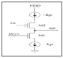
Generally, a Charge Pump is associated with the Phase Frequency Detector. It consists of two CMOS switches controlled by the logic states of PFD terminals, that are respectively Up and Down [2-8-15]. A general Charge Pump structure is shown in Fig.3. The purpose of the Charge Pump is to convert the sequential logic states of the PFD terminals into an analog signal Icp suitable for example to controlling the VCO circuit via a Loop Filter. The Charge Pump injects a constant current Icp to the Loop Filter for a certain period of time equal to the phase difference between Sfdb and Sref.
Fig 3: General Structure of a Charge Pump
[image:2.595.78.270.468.665.2]CMOS implementation of Charge Pump circuit using a simple mirror current is represented in Fig.4. It consists with two CMOS switches formed respectively by PMOS (M4) and NMOS (M1) transistors. PMOS simple mirror current circuit formed by M5 and M6 and NMOS simple mirror current circuit formed of M2 and M3 are used respectively to generate a bias current to the two CMOS switches. The chosen charge pump has simple structure and the number of transistors which consists is reduced compared with other structures recently used [5-6-14].
[image:2.595.333.508.594.753.2]When Up and Down are at low logic level „0‟ then PMOS transistor (M4) conducts and NMOS transistor (M1) turned off and keeps Charge Pump in charging mode, consequently Icp is positive. If Up and Down are at high
logic level „1‟ then NMOS transistor (M1) conducts and PMOS transistor (M4) turned off and keeps Charge Pump in discharge mode, consequently Icp is negative. Finally,
when Up =0 and Down=1 then PMOS (M4) and NMOS (M1) transistors conduct a time equal to a some ps. After this time, Up =1 and Down=0 then PMOS (M4) and NMOS (M1) transistors turned off and keep Charge Pump in neutral mode because the Icp current generated by the Charge Pump is null.
3.3
LOOP FILTER
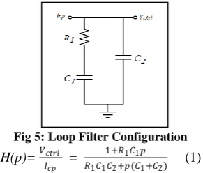
The LF used in the design of CP-PLLs is a second order low pass filter, which converts the current generate from charge pump (𝐼𝑐𝑝) into a controlled voltage signal (𝑉𝑐𝑡𝑟𝑙) for control the VCO after it filters the alternating current component. Also, the LF is used to suppress the noise and high frequency signal components from the CP, and to stabilize the loop [8]. The topology of a low pass filter used in this design is shown in Fig.5 [2], where H (p) is the loop transfer function (1) for Loop Filter.
[image:3.595.313.526.72.534.2]
Fig 5: Loop Filter Configuration
H(p)= 𝑉𝑐𝑡𝑟𝑙 𝐼𝑐𝑝 =
1+𝑅1𝐶1𝑝
𝑅1𝐶1𝐶2+𝑝(𝐶1+𝐶2) (1)
The output voltage of first order RC Loop Filter is irregular because it has voltage jumps due to constant current flow in the resistor. First Order Loop Filter is therefore rarely used; the designer prefers to add a second capacitor to smooth this voltage jumps. The glitch produced by the voltage drop across resistor is dampened by a 𝐶2 capacitor. The capacitor 𝐶2 is used to keep
𝐼𝑐𝑝×𝑅1 from causing voltage jumps in the charge pump
PLL output from occurring [8-12-16].
If the LF components values are not selected correctly, the loop takes too long time to lock, or once the loop is locked small variations in the input data caused the loop to unlock. To calculate correctly the values of capacitors
𝐶1 and 𝐶2 and the resistor 𝑅1, we apply the method proposed by Ken Holladay [17]. This method was also applied successfully in a recent work [18]. We must then define the following parameters:
Frequency Range: 𝐹𝑜𝑠𝑐 𝑚𝑎𝑥=870MHz and
𝐹𝑜𝑠𝑐 𝑚𝑖𝑛=863MHz
Channel Spacing: 𝐿𝑐𝑎𝑛𝑎𝑙=80 kHz
Loop Bandwidth: BPPLL=63KHz
Then, we identify the active component specifications:
VCO sensitivity: 𝐾𝑣𝑐𝑜=7MHz
Charge Pump Current: 𝐼𝑐𝑝 =210µA
[image:3.595.315.525.81.268.2]Table.1 presented below lists the definitions of different terms.
Table 1. Definitions of Terms
Term Description
Fa The frequency of the carrier within the
desired time (Ts) after a step or hop;
normally, 1000 Hz
Fn Natural frequency
Icp Charge-Pump Current
Fstep Maximum frequency change during a step, or
hop, from one frequency to another
Ts The desired time for the carrier to step to a
new frequency
Kvco VCO sensitivity
SFD Damping factor; typically, 0.707
The basic steps and calculations of proposed method [17] are summarized in seven steps.
1- Calculate Maximum Frequency Hop 𝐹𝑠𝑡𝑒𝑝
𝐹𝑠𝑡𝑒𝑝=𝐹𝑜𝑠𝑐 𝑚𝑎𝑥- 𝐹𝑜𝑠𝑐 𝑚𝑖𝑛 (2) 2- Calculate N
N= 𝐹𝐿𝑜𝑠𝑐 𝑚𝑎𝑥
𝑐𝑎𝑛𝑎𝑙 (3)
3- Calculate Natural frequency 𝐹𝑛
𝐹𝑛= 2× BPPLL
2𝜋 +41 (4)
is the damping factor, typically equal to 0.707
4- Calculate 𝐶1 Capacitor
𝐶1=𝑁(2×𝜋×𝐹𝐼𝑐𝑝×𝐾𝑣𝑐𝑜
𝑛)2 (5)
5- Calculate 𝑅1 resistor
𝑅1 = 2× 𝐼 𝑁
𝑐𝑝×𝐾𝑣𝑐𝑜× 𝐶1 (6)
6- Calculate 𝐶2 capacitor
𝐶2 = 10𝐶1 (7)
7- Calculate 𝑇𝑠
𝑇𝑠 = −(𝐿𝑛 𝐹𝑎
𝐹𝑠𝑡𝑒𝑝)
𝐹𝑛×2𝜋×2 (8)
𝐹𝑎is a frequency which is generally equal to 1KHz.
By numerical application, we obtain the following parameter values.
R1 =12Ω
C1 =9.5×10⁻¹²F
C2 = 0.95×10⁻¹²F
3.4
VOLTAGE CONTROLLED
OSCILLATOR
[image:3.595.103.249.332.456.2]Fig 6: Conventional Voltage Controlled Ring Oscillator
IctrlWW4×L6R
6R×L4× Ibias 1
orIctrl WW1×L5
5×L1× Ibias 2
Where (11) expresses the relation between Ibias 1 and
Ibias 2
Ibias 2=WW6×L6R
6R×L6× Ibias 1 (11)
Ibias 1= 𝑉𝑖𝑛 𝑣𝑐𝑜R− 𝑉𝑡𝑛 (12) In classical structure, as shown in Fig.6, the VCO stops oscillating [5], neglecting sub threshold currents, when
𝑉𝑖𝑛 𝑣𝑐𝑜< 𝑉𝑡𝑛+R.𝐼𝑏𝑖𝑎𝑠 1 since the input control voltage
𝑉𝑖𝑛 𝑣𝑐𝑜 is applied to the gate of NMOS transistor (𝑀5𝑅)
and the last is turned off if 𝑉𝑔𝑠< 𝑉𝑡𝑛. This problem
caused a major challenge in VCO designer. To solve this problem and assure a proper functioning of VCO, it is necessary to find a novel VCO structure. It meets the needs of VCO designer and enables to oscillate for each value of control voltage 𝑉𝑖𝑛 𝑣𝑐𝑜 where it is applied at the VCO input signal.
Fig 7: Proposed Voltage Controlled Oscillator
CMOS implementation of a novel VCO design is shown in Fig.7 where five is the number of inverter stages. In the novel design, M2 and M3 operate as an inverter; while the pair transistors formed respectively by M7 and M5, M7 and M1, also M4 and M6 operates as simple mirrors current. A variable bias source current is used to
control the oscillation frequencies of VCO; this current is drained by M8 and is determinate by the values of the input control voltage 𝑉𝑐𝑡𝑟𝑙. M5 and M6 are used to limit the current in VCO. By choosing proper W/L of M5 and M6 current can be limited, and R2 resistor is used to
adjust the current in M8.
In proposed circuit, the control current flowed at each inverter stages is generated by a NMOS simple mirror current , M5 and M7, that replaces a conventional PMOS simple mirror current usually used in recent structures [12-20]. The purpose of mirror current used in the VCO design is to generate and mirror the flowed current at each inverter stages which consists the VCO. Also, in the new VCO design, the input control voltage (𝑉𝑖𝑛 𝑣𝑐𝑜) is
applied at the gate of PMOS transistor, the M8, where in recent work it applied at the gate of NMOS transistor [12- 20]. PMOS transistor is turned on when 𝑉𝑖𝑛 𝑣𝑐𝑜< 𝑉𝑡𝑝, it
is assure that the proposed VCO design oscillate on all range of controlled voltage 𝑉𝑖𝑛 𝑣𝑐𝑜 (0<𝑉𝑖𝑛 𝑣𝑐𝑜<2+ 𝑉𝑡𝑝
-𝑅2×Ibias) varied between 0V to 1.2V, which is difficult to
get from the conventional VCO [5].
The oscillation frequency of VCO is determined by the control current 𝐼𝑐𝑡𝑟𝑙, number of stages N, the amplitude
𝑉𝑜𝑠𝑐 and parasitic capacitance [12-19]. Assume that the
gate parasitic capacitances Cg of the NMOS and PMOS transistors are equal; the oscillation frequency can be found as (13).
Fvco2Nτ1
Where τ is the delay for one stage, which could be given by (14)
τVvco.Cg
Ictrl
Vosc is the oscillation amplitude and Ictrl is the control current. From the above two equations (12) and (13), we can get (15).
Fvco2NVIctrl
oscCg
3.5
DIVIDE BY N COUNTER
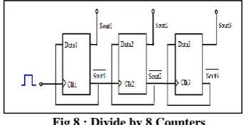
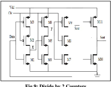
[image:4.595.74.277.519.691.2]The oscillation frequency generated by VCO has been divided via a divide by N before its fed back to the input of PFD block. A programmable divide by N counter is used in the CP-PLL design, which receives a reference clock signal of a predetermined frequency provided via VCO and generates a pulse for every N cycles of the reference clock signal. CMOS implementation of divide by 8 counters, as presented in Fig.8, which is designed by cascading three divide by 2 counters.
Fig 8 : Divide by 8 Counters
A transistor level implementation of a divide by 2 counter [21-23] based on positive edge triggered register in True Single Phased Clocking is shown in Fig.9; it produces one pulse at the output for every two cycles. The True Single-Phase-Clock circuit proposed by Yuan and
Ibias1 Ibias2
[image:4.595.329.501.622.710.2]Svensson [21-22] uses only one clock signal that do not need an inverted clock and fits both static and dynamic CMOS circuit. A same divide by 2 counters was also used in recent work [12-24] to design a DBN counter.
Fig 9: Divide by 2 Counters
A positive latch in TSPC is used in the design of DBN counters. When clock signal is at low logical level (Clk=0), then the input inverter formed respectively by M1 and M3 samples the inverted Data input on the gate of M5 (node X). Consequently, the second inverter is in pre-charge mode, with the M6 transistor charging up node Y to 𝑉𝑑𝑑. The third inverter, which consists of M7
and M9, is in hold mode. This is caused by the two transistors M8 and M9 since they are turned off. Therefore, output S out maintains its previous states, as
well as Sout. To conclude, during low level of the clock
signal,the output of the fourth inverter consists of M10 and M11 transistors holding its previous value and the positive latch is in hold-mode. On the other hand, when clock signal is at high logical level, the dynamic inverter consists of M4 and M6 evaluates. In case where X=1 on the rising edge of the clock signal, node Y discharges. The third inverter composed by M7 and M9 is on during high phase and the node value on Y is passed to Sout. The
S out is equal to Y , S out signal is applied at the input of the third inverter where it‟s the gate of M10 and M11, then it will be inverse to Sout. On the high phase of clock
signal, the node X transitions at a low level if the Data input transitions at a high level. Therefore, the input must be kept stable till the value on node X before the rising edge of the clock propagates to Y.
Contrary to level-sensitive latches, edge triggered registers only sample the input on a clock transition 0 to 1 for a positive edge triggered register. In this way Sout
signal changes only on the rising edge of Clk signal and give half the frequency of the clock signal.
4.
SIMULATION RESULTS
All blocks of CP-PLL are designed and simulated in ADS with 0.35µm AMS CMOS technology that operates at a low power supply 2V. An example of electrical simulation results for all blocks of CP-PLL are presented below. Fig.10 illustrates a transition cycle of the PFD for the different states of its input signals; it‟s the reference signal and the feedback signal. The functioning of Charge Pump is presented in Fig.11; these for different states of PFD terminals. Fig.12 illustrates the charging and discharging period operation mode of Loop Filter, these depending on the sign of this current Icpgenerated by the
Charge Pump. Variation output voltage of the VCO according to the control voltage 𝑉𝑐𝑡𝑟𝑙 is shown in Fig.13.
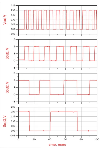
Finally, Fig.14 presents the output signal of the DBN.
Fig 10: Transition Cycle of the PFD
Fig 11: Generate Charge Pump Current
1
0 2
S
re
f,
V
1
0 2
S
fd
b
, V
0 1 2
-1 3
u
p
, V
0 1 2
-1 3
d
o
w
n
, V
0 1 2
-1 3
U
p
, V
20 40 60 80
0 100
0 1 2
-1 3
time, nsec
D
o
w
n
, V
0.0 0.5 1.0 1.5 2.0
-0.5 2.5
U
p
, V
0.0 0.5 1.0 1.5 2.0
-0.5 2.5
D
o
w
n
, V
20 40 60 80
0 100
-200 -100 0 100 200
-300 300
time, nsec
I_
cp
.i,
u
[image:5.595.79.271.120.270.2]Fig 12: Charging and Discharging Period of the Filter
Fig 13: Output Voltage of the VCO
[image:6.595.74.289.71.407.2]Fig 14: Output States of the Divide by 8 Counters
[image:6.595.315.544.473.682.2]Table.2 compares performances and characteristics of the proposed CP-PLLs design to other recent architecture on several items. The table shows that the proposed CP-PLL has a good performance and less area overhead. In addition, we can find that the performance parameters results obtained by proposed of CP-PLLs design is good compared with other CP-PLLs structure.
Table 2 : Performance Characteristics
Parameters This Works [17] [7]
Technology 0.35µm AMS
--- 0.35μ2P4 M
Power Supply 2V --- 3.3V
Icp 210µA 6mA 65µA
R1 12Ω 539Ω 1.38KΩ
C1 9.5pF 1.39 µF 4.845nF
C2 0.95pF 0.139 µF 0.65nF
Range Frequency
870MHz to 863MHz
770MHz to 800MHz
5MHz to 7.5MHz
Lcanal 80 kHz 30KHz ---
BPPLL 63KHz 1KHz ---
KVCO 7MHz/V 22MHz/V 7.1GHz/V
Ratio N divider
8 --- 32
5.
CONCLUSION
In this paper, an effective CP-PLLs architecture has been presented; it is a critical part of the analog-mixed system and RF applications. The presented architecture has two novel design blocks which are respectively Phase Frequency Detector (PFD) and Voltage Controlled Oscillator (VCO). Different results of novel PFD and VCO designs allow verifying its proper operations, and
-200 -100 0 100 200
-300 300
I_
cp
.i,
u
A
20 40 60 80
0 100
700 750 800 850 900
650 950
time, nsec
V
ct
rl,
m
V
700 750 800 850 900
650 950
V
c
tr
l,
m
V
20 40 60 80
0 100
0.0 0.5 1.0 1.5 2.0
-0.5 2.5
time, nsec
V
o
u
t,
V
0.0 0.5 1.0 1.5 2.0
-0.5 2.5
V
ou
t,
V
0 1 2
-1 3
S
ou
t1
, V
0 1 2
-1 3
S
ou
t2
, V
20 40 60 80
0 100
0.0 0.5 1.0 1.5 2.0
-0.5 2.5
time, nsec
S
ou
t3
they are implemented into CP-PLLs design. The results obtained by electrical simulations allow validating the proper functioning of proposed CP-PLLs architecture. They show a good performance characteristics of the proposed circuit; where uses relatively small-size devices and low power supply 2V to operate in a large range frequency, and less area overhead. The performances parameters of CP-PLLs are evaluated in ADS, all blocks of the proposed architecture has presented in this paper are designed with 0.35μm AMS CMOS technology.
6.
ACKNOWLEDGMENTS
This work was supported by Laboratory of Electronic and Micro-technology Communication (EMC), National School of Engineering Sfax, University of Sfax, Tunisia.
7.
REFERENCES
[1] B Razavi, Monolithic, Phase-Locked Loops and Clock Recovery Circuits; Theory and Design, IEEE Press 1996.
[2] F.M. Gardner, Phase Lock Techniques, 2nd ed., New York, Wiley, 1979.
[3] C. Munker, B.-U. Klepser, B. Neurauter, and C. Mayer, Digital RF CMOS transceivers for GPRS and EDGE, in IEEE Radio Frequency Integrated Circuits (RFIC) Symp. Dig. of Papers, 2005, pp. 265–268.
[4] Intissar Toihria, Rim Ayadi and Mohamed Masmoudi, An Effective CMOS Charge Pump-Phase Frequency Detector Circuit for PLLs Applications, International Multi-Conference on Systems, Signals & Devices (SSD) Hammamet, Tunisia, March 18-21, 2013
[5] Chun-Lung Hsu, IEEE Member, Yiting Lai, and Shu-Wei Wang, Built-In Self-Test for Phase-Locked Loops. IEEE Transactions on instrumentation and measurement, VOL. 54, NO. 3, JUNE 2005.
[6] Debashis Mandal and T. K. Bhattacharyya, Implementation of CMOS Low-power Integer-N Frequency Synthesizer for SOC Design, Journal of Computers, VOL. 3, NO. 4, Avril 2008.
[7] Deng Wen-Juan, Liu Shubo, Wang Song, Chen Jian, Zou Jijun, On The Design Of The Charge Pump PLL In Video Decoder, Journal of Theoretical and Applied Information Technology, 15th October 2012. Vol. 44 No.1
[8] F. M. Gardner, Charge-Pump Phase-Lock Loops, IEEE Trans. Communication, vol. COM-28, 1849– 1858, Nov. 1980.
[9] C. A. Sharpe, A 3-state phase detector can improve your next PLL design, EDN, pp. 55-59, Sept. 1976.
[10] Dirk Pfaff, Frequency Synthesis for Wireless Transceivers, Swiss Federal Institute of Technology Zurich, 2003.
[11] J.-J. Charlot, N. Milet-Lewis, T. Zimmer and H. Lévi (BEAMS Association). VHDL-AMS for mixed technology and mixed signal, an overview.
[12] A Novel Built-In Self-Test Architecture for Charge-Pump Phase Locked Loops. J. Ramesh and K.Gunavathi. ICGST-PDCS Journal, Volume 7, Issue 1, May, 2007
[13] Ashish Tiwari, Prof Anil Kumar Sahu, Dr.G.R.Sinha, Design for Testability architecture using the existing elements of CP-PLL for Digital Testing Applications in VLSI ASIC Design, International Journal of VLSI & Signal Processing Applications, Vol.2,Issue 1, Feb 2012, (56-64).
[14] Hsiang-Hui Chang, Student Member, IEEE, Jyh-Woei Lin, Ching-Yuan Yang, Member, IEEE, and Shen-Iuan Liu, Member, Wide-Range Delay-Locked Loop With a Fixed Latency of One Clock Cycle, IEEE. IEEE Journal of Solid-State Circuits, VOL. 37, NO. 8, AUGUST 2002
[15] Jyoti Gupta Ankur Sangal and Hemlata Verma High Speed CMOS Charge Pump Circuit for PLL Applications Using 90nm CMOS Technology. World Applied Sciences Journal 16(Special Issue on Recent Trends in VLSI Design): 63-69, 2012 ISSN 1818-4952 IDOSI Publications, 2012.
[16] Pascal ACCO, Etude de la boucle à verrouillage de phase par impulsions de charge Prise en compte des aspects hybrides, Décembre 2003.
[17] K. Holladay, Design a PLL for specific loop bandwidth, END EUROPE, pp 64-66, October 2000
[18] Ahmed FAKHFAKH, Contribution à la modélisation comportementale des circuits radiofréquence, 11 Janvier 2002
[19] Retdian, N., Takagi, S. and Fujii, N., “Voltage controlled ring oscillator with wide tuning range and fast voltage swing”, IEEE Asia-Pacific Conference, ASIC on 2002. Proceedings, pp 201 – 204, Aug. 2002.
[20] Florence Azaïs, Yves Bertrand, and Michel Renovell, André Ivanov and Sassan Tabatabaei, An All-Digital DFT Scheme for Testing Catastrophic Faults in PLLs, IEEE Design & Test of Computers January–February 2003
[21] Jiren Yuan and Christer Svensson, High-Speed CMOS Circuit Technique, IEEE Journal of Solid-State Circuits. VOL.24, NO.1, FEBRARY 1989.
[22] Jiren Yuan and Christer Svensson, New Single-Clock CMOS Latches and Flip-Flops with Improved Speed and Power Savings, IEEE Journal of Solid-State Circuits. VOL. 32, NO.1, FEBRARY 1997.
[23] Designing Sequential Logic Circuits, chapitre7