University of South Carolina
Scholar Commons
Theses and Dissertations
2015
III-V Nitride Based Microcantilever Heaters for
Unique Multimodal Detection of Volatile Organic
Compounds at Low Temperature
Ifat Jahangir
University of South Carolina
Follow this and additional works at:https://scholarcommons.sc.edu/etd
Part of theElectrical and Electronics Commons
This Open Access Thesis is brought to you by Scholar Commons. It has been accepted for inclusion in Theses and Dissertations by an authorized administrator of Scholar Commons. For more information, please [email protected].
Recommended Citation
III-V Nitride based microcantilever heaters for unique multimodal detection of volatile
organic compounds at low temperature
by
Ifat Jahangir
Bachelor of Science in Engineering
Bangladesh University of Engineering and Technology, 2011
Submitted in Partial Fulfillment of the Requirements
For the Degree of Master of Science in
Electrical Engineering
College of Engineering and Computing
University of South Carolina
2015
Accepted by:
Goutam Koley, Director of Thesis
MVS Chandrashekhar, Reader
Dedication
Acknowledgements
I would like to thank my Supervisor Dr. Goutam Koley for supporting me during
these three years. Working with Dr. Koley, in my opinion, is the best thing that a MS
student can wish for. He perfectly translates the character of his students and provides the
best conditions for the development of intellectual qualities and creative thinking. I am
very grateful to him for his scientific advice and knowledge and many insightful
discussions and suggestions he provided me and beyond all his guidance in my tough
times.
I owe my gratitude to Dr. MVS Chandrashekhar, member of my thesis defense
committee, for his guidance and support during the last one year. Although I am currently
a PhD student in his group working in a different area, he still managed time to help me
with my MS research project whenever needed.
The Microfabrication part was done using the class 10/100 cleanroom facilities at
the IEN at Georgia Institute of Technology. I worked there from April to July, 2014 and
met really nice, helpful and knowledgable people and stuff. I would like to express my
gratitude to Prof. David Gottfried, Dr. Gary Spinner, Dr. Mikkel Thomas, Thomas
Johnson Averette, Charlie Suh, Charlie Turgeon and Tran-Vinh Nguyen for their help in
troubleshooting various problems that I faced there.
I would like to acknowledge the financial support from NSF grant that funded
Sultana specially, for their help with fabrication. Hafiz and I worked together in IEN
facilities and shared a process flow that we both developed during our stay there. Without
his direct help and the guidance from his wife, who had great experience in III-V Nitride
device fabrication, it would not be possible to complete the mammoth task that I took on.
I would also like to thank our alumni Dr. Ehtesham Bin Quddus, Dr. Md. Qazi, Dr. Md.
Waliullah Khan Nomani and Dr. Jie Liu for sharing their valuable experience of working
in IEN with me to make better devices than the previous attempts. I would also like to
thank Dr. Amol Singh, Dr. Md. Ahsan Uddin, Dr. Yihao Zhu, Dr. Alina Wilson, Nick
DeRoller, Rina Patel and James Tolson for their constant support throughout the last
three years.
I wish to express my heartfelt gratitude to my family – my parents and my
brother, for always having faith in me and for bringing me this far. I would also like to
thank all my friends who were very supportive during the entire duration of my stay here
in Columbia, South Carolina. Finally and most importantly, I would like to express my
deep gratitude towoards the Almighty for giving me the ability to finish this work
Abstract
Detection of volatile organic compounds (VOCs), which are widely used in
industrial processes and household products, is very important due to significant health
hazards associated with them. VOCs are commonly detected using photo-ionization
detectors (PIDs),suspended hot bead pellistors,or heated metal oxide semiconductor
functionalization layers. However, these techniques used for detecting VOCs often suffer
from one or more of the following issues - high power consumption, limited selectivity,
complicated functionalization technique and expensive characterization tools. On the
other hand, microcantilevers offer excellent avenues for molecular sensing that arises out
of their high sensitivity to various physical parameter changes induced by the analyte
molecules. Microcantilever heaters, which are extremely sensitive to changes in thermal
parameters, have been widely utilized for calorimetry, thermal nanotopography and
thermal conductivity measurements. Due to the small area of the microcantilever that
needs to be heated (i.e. the tip of a triangular microcantilever), they also offer the
possibility of reduced power consumption for high temperature operation. The present
study reports the multimodal VOC detection capability of unfunctionalized
microcantilever heaters made of AlGaN/GaN heterostructure, which can address many of
the limitations observed in other techniques.
The microcantilevers, fabricated on an AlGaN/GaN on Si wafer, were found to be
single conducting channel along the arms, some were specially designed to have two
parallel channels, isolated by semi-insulating GaN or air. The single channel
microcantilevers exhibited a dc response to different VOCs above particular threshold
voltages, which were found out to be strongly correlated to the latent heat of evaporation
for those analytes. At a constant dc bias which is above that threshold voltage, the
magnitude of the response for any VOC is a function of concentration and molecular
dipole moment of the VOC, which is another metric that can be easily determined and
calibrated. While threshold voltage is a reliable indicator for uniquely identifying a VOC,
the response magnitude can be used to estimate the concentration of the analyte also,
down to low ppm range with a response time less than 40 s. The microcantilevers with
two parallel channels are suitable for thermal conductivity based detection of any vapor
or gas, therefore it helps pinpointing the VOCs even better in an event where two
different VOCs have very close threshold voltages but significantly different thermal
conductivities. A numerical model, based on three dimensional heat transfer and Joule
heating equations, has also been developed for these microcantilevers. This model has
been employed to explain the physical phenomena associated with the sensor under
different bias conditions, and also to predict the response time of the heater alone, which
is much smaller than the response time of the overall system. The noise limited resolution
from the theoretical model is in the range of parts per billion and shows excellent promise
for the future application of this kind of sensor in detecting VOCs with very low power
Table of Contents
Dedication………..iii
Acknowledgements ... iv
Abstract……….vi
List of Figures ... x
List of Tables ... xiv
Chapter 1 Introduction... 1
1.1 Overview ... 1
1.2 Chemical sensor arrays... 3
1.3 Classification of sensors ... 4
1.4 Chemical sensors for environmental monitoring ... 9
1.5 Microcantilever heater based environmental sensors... 12
Chapter 2 Fabrication of AlGaN/GaN Microcantilever Heaters ... 15
2.1 Wafer information ... 16
2.2 Mask design... 18
2.3 Details of the fabrication steps ... 19
Chapter 3 Experimental Setup and Modeling... 43
3.1 Electrical characterization and sensing setup ... 43
3.2 Thermal characterization setup ... 47
3.3 Simulation model ... 50
Chapter 4 Results and Discussions ... 54
4.1 Electrical Characterization Results ... 54
4.2 Sensing and Thermal Characterization Results ... 57
4.3 Simulation Results... 73
Chapter 5 Conclusion ... 81
References……….83
List of Figures
Figure 1.1 Various applications of chemical sensors... 9
Figure 2.1 (a) Scanning electron microscope (SEM) and (b) infrared (IR) microscope images of the fabricated heated cantilever, indicating heating only near the free end of the cantilever [7]. ... 16
Figure 2.2 Different layers of the AlGaN/GaN wafer grown on Si (111) substrate with mesa and cantilever layer as shown. ... 17
Figure 2.3 Mask layout - the final design including all the layers superimposed showing the schematic of the final outcome of the fabricated devices. The mask design has the provision for auto dicing each sample into several chips. ... 18
Figure 2.4 Process flow diagram of top GaN microcantilever. (a) A diced AlGaN/GaN on Si sample; (b) PECVD SiO2 (300 - 400 nm) deposition; (c) Coat sample with SC1827
photoresist; (d) Pattern photoresist; (e) Pattern the mesa layer with ICP etching of oxide; (f) ICP etching of AlGaN; (g) Remove oxide using BOE; (h) PECVD SiO2 (1.2 µm)
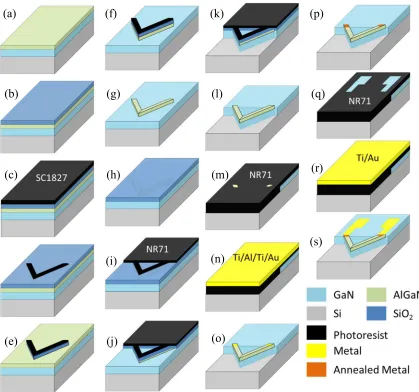
deposition; (i) Pattern cantilever outline with NR71 photoresist; (j) ICP etching of oxide; (k) ICP etching of GaN; (l) Oxide etching with BOE; (m) Pattern Ohmic Contact using NR71; (n) E-beam deposition of Ti/Al/Ti/Au metal stack; (o) Lift-off of ohmic layer; (p) Rapid thermal annealing of ohmic contacts; (q) Pattern probe contact using NR71; (r) E-beam deposition of Ti/Au metal stack; (m) Lift-off of probe contact layer. ... 21
Figure 2.5 Optical images taken at various stages of fabrication: (a) Mesa outline; (b) Cantilever outline; (c) Ohmic contact deposition; (d) Probe contact deposition. ... 22
Figure 2.6 Working principle of Bosch process: passivation cycle and etch cycle. ... 23
Figure 2.7 Process flow diagram of through wafer Si etching from backside using Bosch process. (a) A flipped sample - thinning down the Si substrate (~ 400 µm) in ICP ; (b) PECVD SiO2 (4 µm thick) deposition; (c) Photoresist NR5-8000 (8 µm thick) coating;
(d) Pattern the resist layer and etch SiO2 in RIE; (e) Through wafer Si etching in ICP
using Bosch process; (f) Schematics of the released GaN. ... 26
Figure 2.9 Photograph of samples (top) after patterning resist on the PECVD oxide (bottom) after etching the oxide in RIE. ... 31
Figure 2.10 Photograph of samples (top) after through wafer Si etching; (bottom) auto-diced into smaller chips. ... 32
Figure 2.11 Photograph of samples comparing the releasing of microcantilevers with two different techniques which shows the incompatibility and inapplicability of the old technique for processing sophisticated designs. ... 33
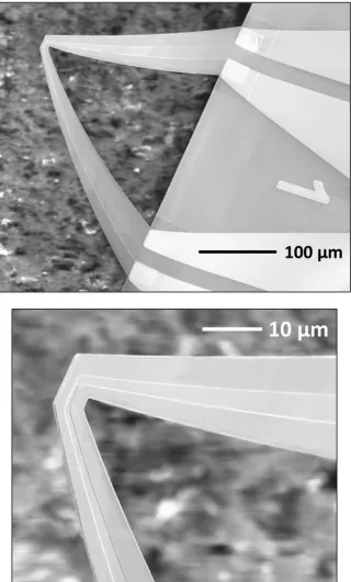
Figure 2.12 Optical image of the top outline showing the single channel microcantilever heaters. ... 33
Figure 2.13 Optical image of the top outline showing the (top) dual channel microcantilever heaters and (bottom) compound microheater structures. ... 34
Figure 2.14 Optical image of the top outline showing the micro hotplates. ... 35
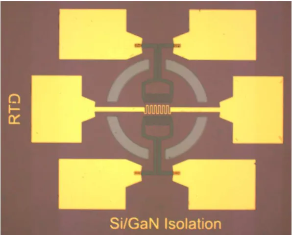
Figure 2.15 Optical image of the microhotplate with resistance temperature detector (RTD). ... 35
Figure 2.16 Optical image of the entire top outline ... 36
Figure 2.17 SEM image of single channel microcantilever heaters, (top) from top; (bottom) from an angle. ... 37
Figure 2.18 SEM image of (top) single channel triangular microcantilever heater (SC-TMH); (bottom) close-up of the tip. ... 38
Figure 2.19 SEM image of dual channel and compound microcantilever heaters, (top) from top; (bottom) from an angle. ... 39
Figure 2.20 SEM image miscellaneous microheater elements: (top) zigzag microheater; (middle) Microhotplate; (bottom) close-up of the heating elements shown above. ... 40
Figure 2.21 SEM image of (top) continuous tip dual channel microcantilever heater (CTDC-TMH); (bottom) close-up of the tip. ... 41
Figure 2.22 SEM image of (top) split tip dual channel microcantilever heater (CTDC-TMH); (bottom) close-up of the tip. ... 42
Figure 3.1 VOC sensing setup. ... 44
Figure 3.2 Bias and exposure configuration for SC-TMH sensing experiments: (top) Transient mode; (bottom) Steady-state mode. ... 45
Figure 3.3 Steady-state operating modes of the DC-TMH: (left) Self-heating mode; (right) Secondary heating mode. ... 46
Figure 3.5 (a) Raman spectra of the heated cantilever for 300, 400, 500 and 600 K temperature on the hot plate. E2 Peak becomes wider as temperature increases. (b) Shift
in E2 and A1(LO) peaks towards lower wave number as temperature goes up. ... 48
Figure 3.6 Infrared (IR) thermal microscopy setup. ... 50
Figure 3.7 Variation of local resistivity as a function of temperature. ... 52
Figure 4.1 I-V characteristics for a SC-TMH device. ... 54
Figure 4.2 I-V characteristics for a SC-TMH device. ... 55
Figure 4.3 TLM contact pads, before annealing and after annealing ... 56
Figure 4.4 The total resistance between contacts as a function of distance ... 56
Figure 4.5 IR microscopy image of a first generation SC-TMH device with 50 V dc bias. (a) In air; (b) In 2000 ppm isopropanol vapor. ... 57
Figure 4.6 Line scan along the cantilever arm shown in the IR microscopy image of a first generation SC-TMH device with 50 V dc bias in Figure 4.5. Inset shows an equivalent circuit model of the cantilever. ... 58
Figure 4.7 Response of a SC- TMH sensor to 500 ppm of formaldehyde at 10 V dc bias. Current magnitude changed by 2.17% with rise time and fall time of 8 s and 13 s respectively. Two sensing cycles are shown here to demonstrate repeatability. ... 59
Figure 4.8 Normalized change of current (%) for the SC-TMH device at different dc biases and with analyte concentration of 2000 ppm. ... 61
Figure 4.9 Dependence of threshold voltage of detection on latent heat of evaporation of VOCs. The error bars indicate the range of values recorded for different concentrations within a range of 100-2000 ppm. All threshold voltages are below 5 V. ... 65
Figure 4.10 Detectability of threshold voltage at low concentration. The response at threshold voltage is determined using the equation given below. Extrapolating the threshold response vs. concentration curves, we find the noise limited resolution to be around 1.5 ppm with 0.022% being the rms noise magnitude. ... 66
Figure 4.11 Normalized change of Current for three different concentrations, shown as a function of dipole moment. ... 67
Figure 4.12 Effect of polarization on sensor response evident using a SC-TMH sensor covered with 10 nm thick PECVD SiO2: (a) Vth vs ΔHvap shows an upward shift in Vth; (b) No correlation with response magnitude with dipole moment. ... 70
Figure 4.14 Simulated temperature profile for SC-TMH under 10 V dc bias, in UHP N2
and 1% isopropanol... 74
Figure 4.15 Temperature profile line scan along the length of the SC-TMH, extracted from Figure 4.14. ... 74
Figure 4.16 Simulated peak temperature of SC-TMH as a function of applied bias with or without analyte vapor flow (1% isopropanol). ... 75
Figure 4.17 Simulated temperature profile for continuous tip DC-TMH under 10 V dc bias, in (a) UHP N2 and (b) 1% isopropanol. ... 76
Figure 4.18 Simulated temperature profile (line scan along the length of the cantilever) for continuous tip DC-TMH under 10 V dc bias, in (a) UHP N2 and (b) 1%
isopropanol. ... 77
Figure 4.19 Simulated temperature profile for split tip DC-TMH under 10 V dc bias, in (a) UHP N2 and (b) 1% isopropanol. ... 78
Figure 4.20 Simulated temperature profile (line scan along the length of the cantilever) for split tip DC-TMH under 10 V dc bias, in (a) UHP N2 and (b) 1% isopropanol. ... 79
List of Tables
Table 4.1 Calculated parameters from the TLM test ... 56
Table 4.2 Dipole Moment (µ) and Latent Heat of Evaporation (Hvap) of VOCs ... 62
Table 4.3 Sensitivity, rise time and fall time for different analytes at threshold voltage. ... 67
Introduction
1.1
Overview
Detection of small quantities of molecules is of significant interest for numerous
numbers of applications, ranging from gas sensing and environmental monitoring to
biological and medical diagnostics. These require the sensors to be inexpensive, power
efficient, easily deployable and miniaturized, yet sensitive enough to detect molecules
down to the single-molecule level. With the advancement of miniaturization technologies
molecular sensors are getting smaller and smaller in dimensions. Miniaturization is also
essential for in vivo physiological monitoring, sensor portability and minimized sample
volumes. Conventional molecular sensors suffer from extensive packaging, complex
electronic interfacing and regular maintenance, the use of novel Microlectromechanical
systems (MEMS) devices that integrate electronics and micro-mechanical structures on
chip could address all those drawbacks.
Microcantilevers are the most simplified MEMS based devices. Diverse
applications of microcantilevers in the field of sensors have been explored by many
researchers. These sensors have several advantages over the conventional techniques in
terms of high sensitivity, low cost, simple procedure, non-hazardous procedures and
quick response. A molecular sensor is usually evaluated with respect to three major
high sensitivity towards targeting chemicals, excellent selectivity to a specific signal of
interest, and a very small dimension.
In this work we are proposing molecular sensors that will be made of novel
V-shaped micro-cantilevers, in the form of arrays in a chip. Due to their reduced dimension,
many of the individual cantilevers can be integrated together in a chip, thus the final
device is miniaturized.
Particles that are smaller than the characteristic lengths associated with the
specific phenomena often display new chemistry and new physics that lead to new
properties that depend on size. The analyte molecules and the sensing elements are of
comparable size for microcantilever based sensing which promotes better sensitivity.
Again in the case of nanoscale sensors the size of the structure is reduced further, surface
to volume ratio increases considerably and the surface phenomena predominate over the
chemistry and physics in the bulk. This enhances the sensitivity even more since the
molecular interaction or sensing occurs at the surface.
The careful selection of superior material quality confirms the fast response.
AlGaN/GaN heterostructures contain a highly conductive two-dimensional electron gas
(2DEG) at the interface, which is sensitive to mechanical load, as well as to chemical
modification of the surface, and can be used for novel sensing principles and as
transducers for MEMS applications. The selectivity of the sensor is improved by the
multimodal detection technique apart from the nature of the gas molecules themselves. In
multimodal detection technique independent parameters can be independently measured
and while they are combined together a unique signature for any particular molecule is
1.2
Chemical sensor arrays
A chemical sensor is a device that transforms chemical information, ranging from
the concentration of a specific sample component to total composition analysis, into an
analytically useful signal. The chemical information, mentioned above, may originate
from a chemical reaction of the analyte or from a physical property of the system
investigated.
A physical sensor is a device that provides information about a physical property
of the system. A chemical sensor is an essential component of an analyzer. In addition to
the sensor, the analyzer may contain devices that perform the following functions:
sampling, sample transport, signal processing, data processing. An analyzer may be an
essential part of an automated system. The analyzer working according to a sampling
plan as a function of time acts as a monitor.
Chemical sensors contain two basic functional units: a receptor part and a
transducer part. Some sensors may include a separator which is, for example, a
membrane. In the recepror part of a sensor the chemical information is transformed into a
form of energy which may be measured by the transducer.
The transducer part is a device capable of transforming the energy carrying the
chemical information about the sample into a useful analytical signal. The transducer as
such does not show selectivity.
Physical, where no chemical reaction takes place. Typical examples are those
based upon measurement of absorbance, refractive index, conductivity, temperature or
mass change.
Chemical, in which a chemical reaction with participation of the analyte gives rise
to the analytical signal.
Biochemical, in which a biochemical process is the source of the analytical signal.
Typical examples are microbial potentiometric sensors or immunosensors. They may be
regarded as a subgroup of the chemical ones. Such sensors are called biosensors.
In some cases it is not possible to decide unequivocally whether a sensor operates
on a chemical or on a physical principle. This is, for example, the case when the signal is
due to an adsorption process.
Sensors are normally designed to operate under well-defined conditions for
specified analytes in certain sample types. Therefore, it is not always necessary that a
sensor responds specifically to a certain analyte. Under carefully controlled operating
conditions, the analyte signal may be independent of other sample components, thus
allowing the determination of the analyte without any major preliminary treatment of the
sample. Otherwise unspecific but satisfactory reproducible sensors can be used in series
for multicomponent analysis using multivariate calibration software and signal
processing. Such systems for multicomponent analysis are called sensor arrays.
1.3
Classification of sensors
The development of instrumentation, microelectronics and computers makes it
principles that have been used in chemistry.
Chemical sensors may be classified according to the operating principle of the
transducer:
1. Optical devices transform changes of optical phenomena, which are the result
of an interaction of the analyte with the receptor part. This group may be further
subdivided according to the type of optical properties which have been applied in
chemical sensors:
a) Absorbance, measured in a transparent medium, caused by the absorptivity of the
analyte itself or by a reaction with some suitable indicator.
b) Reflectance is measured in non-transparent media, usually using an immobilized
indicator.
c) Luminescence, based on the measurement of the intensity of light emitted by a
chemical reaction in the receptor system.
d) Fluorescence, measured as the positive emission effect caused by irradiation. Also,
selective quenching of fluorescence may bethe basis of such devices.
e) Refractive index, measured as the result of a change in solution composition. This
may include also a surface plasmon resonance effect.
f) Optothermal effect, based on a measurement of the thermal effect caused by light
absorption.
g) Light scattering, based on effects caused by particles of definite size present in the
2. Electrochemical devices transform the effect of the electrochemical interaction
analyte – electrode into a useful signal. Such effects may be stimulated electrically or
may result in a spontaneous interaction at the zero-current condition. The following
subgroups may bedistinguished:
a) Voltammetric sensors, including amperometric devices, in which
current is measured in the d.c. or a.c. mode. This subgroup may include sensors
based on chemically inert electrodes, chemically active electrodes and modified
electrodes. In this group are included sensors with and without (galvanic sensors)
external current source.
b)Potentiometric sensors, in which the potential of the indicator electrode
(ion-selective electrode, redox electrode, metaVmeta1 oxide electrode) is
measured against a reference electrode.
c) Chemically sensitized field effect transistor (CHEMFET) in which the
effect of the interaction between the analyte and the active coating is transformed
into a change of the source-drain current. The interactions between the analyte
and the coating are, from the chemical point of view, similar to those found in
potentiometric ion-selective sensors.
d) Potentiometric solid electrolyte gas sensors, differing from class 2(b)
because they work in high temperature solid electrolytes and are usually applied
3. Electrical devices based on measurements, where no electrochemical processes
take place, but the signal arises from the change of electrical properties caused by the
interaction of the analyte.
a) Metal oxide semiconductor sensors used principally as gas phase
detectors, based on reversible redox processes of analyte gas components.
b) Organic semiconductor sensors, based on the formation of charge
transfer complexes, which modify the charge carrier density.
c) Electrolytic conductivity sensors.
d) Electric permittivity sensors.
4. Mass sensitive devices transform the mass change at a specially modified
surface into a change of a property of the support material. The mass change is caused by
accumulation of the analyte.
a) Piezoelectric devices used mainly in gaseous phase, but also in
solutions, are based on the measurement the frequency change of the quartz
oscillator plate caused by adsorption of a mass of the analyte at the oscillator.
b) Surface acoustic wave devices depend on the modification of the
propagation velocity of a generated acoustical wave affected by the deposition of
a definite mass of the analyte.
5. Magnetic devices based on the change of paramagnetic properties of a gas
being analysed. These are represented by certain types of oxygen monitors.
6. Thermometric devices based on the measurement of the heat effects of a
effects may be measured in various ways, for example in the so called catalytic sensors
the heat of a combustion reaction or an enzymatic reaction is measured by use of a
thermistor. The devices based on measuring optothermal effects can alternatively be
included in this group.
This classification represents one of the possible alternatives. Sensors have, for
example, been classified not according to the primary effect but to the method used for
measuring the effect. As an example can be given the so-called catalytic devices in which
the heat effect evolved in the primary process is measured by the change in the
conductivity of a thermistor. Also, the electrical devices are often put into one category
together with the electrochemical devices.
Sensors have also been classified according to the application to detect or
determine a given analyte. Examples are sensors for pH, for metal ions or for determining
oxygen or other gases. Another basis for the classification of chemical sensors may be
according to the mode of application, for example sensors intended for use in vivo, or
sensors for process monitoring and so on. It is, of course, possible to use various
classifications as long as they are based on clearly defined and logically arranged
principles.
The biosensors are not presented as a special class because the process on which
they are based is, in general, common to chemical sensors. They may be also
differentiated according to the biological elements used in the receptor. Those may be:
organisms, tissues, cells, organelles, membranes, enzymes, antibodies, etc. The
biosensors may have several enzymatic systems coupled which serve for amplification of
1.4
Chemical sensors for environmental monitoring
Figure 1.1 shows various applications of chemical sensors including monitoring
automobile emission gasses, medical diagnosis, industrial control, national security,
indoor air quality control, and environmental evaluation.
The regulation on automobile emission usually involves toxic gases such as
nitrogen oxide (NOx), carbon monoxide (CO), or volatile hydrocarbons.
A general medical examination requires measuring these substances in human
body such as glucose, blood oxygen, and cholesterol, which lead to determine possible
disease or disorder of a patient.
In a research lab or industrial factory, it is extremely important to prevent
accidents from leakage of flammable gases such as H2, thus the concentration of H2 on
working sites needs to be monitored in real-time.
There are indoor air pollutants such as volatile organic compounds (VOCs)
including acetone, ethanol and isopropanol. These organic compounds are widely used as
ingredients in household products and extensive exposure to these VOCs can lead to
disorder, sickness or even death [1].
Particularly, there have been significant increasing technical demands on
indentifying explosive chemicals due to challenges of anti-terrorism worldwide. Sensors
are required to be deployed at public transport station, plaza, schools, and commercial
buildings to detect trace amount of explosive molecule such as TNT, DNT, and RDX [2].
Apart from explosive chemicals, recently in last few decades there have been several
incidents of the use of CWAs (mustard gas, sarin, etc.) around the world that killed
thousands of lives and threatened the whole civilization [3]. These incidents worldwide
highlight the importance of having a continuous detection and monitoring of these kinds
of chemical agents and explosives for both defense and homeland security.
Chemical sensors are expected to play a critical role in environmental monitoring
(both indoor and outdoor) and environmental control (air, water), facilitating a better
quality of life. The projected increase in global energy usage and unwanted release of
pollutants has led to a serious focus on advanced monitoring technologies for
environmental protection, remediation, and restoration. In a recent study, the World
Health Organization (WHO) reported that over 3 million people die each year from the
effects of air pollution. Furthermore, reports from World Energy Congress (WEC)
suggest that if the world continues to use fuels reserves at the current rate, the
environmental pollution in 2025 will create irreversible environmental damage.
alters cardiac function. Within the general population, medical studies suggest that
inhaling particulate matter (PM) is associated with increased mortality rates which are
further magnified for people suffering from diabetes, chronic pulmonary diseases, and
inflammatory diseases. Pollution, in general is contamination that renders part of the
environment unfit for intended or desired use. Natural processes release toxic chemicals
into the environment as a result of ongoing industrialization and urbanization. Major
contributors to large-scale pollution crisis are deforestation, polluted rivers, and
contaminated soils. Other sources of pollution include emissions from iron and steel
mills; zinc, lead, and copper smelters; municipal incinerators; oil refineries; cement
plants; and nitric and sulphuric acid producing industries. Of the group of pollutants that
contaminate urban air, nitrous oxide (NOx), fine suspended PM, sulphur dioxide (SO2),
and ozone pose the most widespread and acute risks. Recent studies on the effects of
chronic exposure to air pollution have singled out PM suspended in smog (NOx) and
volatile organic compounds (VOCs) as the pollutant most responsible for life-shortening
respiratory and associated health disorders. Since the Clean Air Act was adopted in 1970,
great strides have been made in the U.S. in reducing many harmful pollutants from air,
such as SO2. Levels of NOx, however, have increased by 20% over the last 30 years.
Sources of NOx include passenger vehicles, industrial facilities, construction equipment
and railroads, but of the 25 million tons of NOx discharged annually in the U.S., 21% of
that amount is generated by power plants alone, resulting in rising threats to the health of
the general population. Furthermore, the SCanning Imaging Absorption SpectroMeter for
Atmospheric CHartographY (SCIAMACHY), shows rapid increase in NOx columns
Rapid detection of contaminants in the environment by emerging technologies is
of paramount significance. Environmental pollution in developing countries has reached
an alarming level thus necessitating deployment of real-time pollution monitoring
sensors, sensor networks, and real-time monitoring devices and stations to gain a
thorough understanding of cause and effect. A tool providing interactive qualitative and
quantitative information about pollution is essential for policy makers to protect massive
populations, especially in developing countries.
1.5
Microcantilever heater based environmental sensors
Detection of volatile organic compounds (VOCs), which are widely used in
industrial processes and household products, is very important due to significant health
hazards associated with them.[1] VOCs are commonly detected using photo-ionization
detectors (PIDs),[2] suspended hot bead pellistors,[3] or heated metal oxide
semiconductor functionalization layers.[4]-[7] The detection methodology using PIDs is
based on high-energy photon (typically > 10.5 eV) induced ion generation, while that
using hot bead pellistors takes advantage of the exothermic reaction (from auto-ignition
of VOCs) to produce a change in resistance. Heated metal oxide (i.e. TiO2 or SnO2)
based sensing also relies upon a change is resistance, but at a temperature below the
auto-ignition temperature of the VOCs. However, all the above techniques suffer from the
problem of high power requirement as well as poor selectivity among VOCs, which is
often important for proper identification of the source of a problem. Although the last
method requires somewhat lower operational power, it involves complicated
Microcantilevers offer excellent avenues for molecular sensing that arises out of
their high sensitivity to various physical parameter changes induced by the analyte
molecules.[8]-[15] Microcantilever heaters, which are extremely sensitive to changes in
thermal parameters,[16]-[21] have been widely utilized for calorimetry,[16] thermal
nanotopography[17] and thermal conductivity measurements.[18] Due to the small area
of the microcantilever that needs to be heated (i.e. the tip of a triangular microcantilever),
they also offer the possibility of reduced power consumption for high temperature
operation. However, achieving repeatable and reliable functionalization of a
microcantilever, especially over a small area, is a challenge that has thwarted practical
applications of microcantilever based sensors. On the other hand, unfunctionalized
microcantilevers (typically made of Si) are not particularly sensitive toward a specific
analyte, and are generally accepted to be incapable of performing selective detection.
Thus, only a handful of studies utilizing uncoated microcantilevers to perform unique
molecular detection have been reported so far.[13], [22], [23] In these studies, detection
is generally based on changes in physical properties of the media surrounding the
cantilever (i.e. viscosity,[23] thermal conductivity,[22] or the analyte (i.e. deflagration
temperature[22]). However, these techniques are applicable only to a few specific
analytes, and selective detection still remains a major challenge, especially when the
analytes are diluted (or present in minute quantities) or have similar physical properties
i.e. VOCs.
III-Nitride heterojunction (especially AlGaN/GaN) based microcantilevers offers
a unique opportunity for realizing these microscale heaters, taking advantage of presence
highly efficient surface heating. In addition, strong spontaneous polarization of
III-Nitride surfaces allows these heaters to interact better with VOCs, which are typically
strongly polar in nature. Finally, AlGaN/GaN heterojuntion based heaters are capable of
operating at high temperature and harsh environment due to chemical inertness and wide
bandgap of III-Nitrides. With commercial availability of high quality III-Nitride
heterojunciton epilayers on Si, the fabrication of these heaters is also quite
straightforward. Although, III-Nitride based microcantilevers have been demonstrated
earlier,[11], [25], [26] there is no report so far on triangular microcantilever heaters and
Fabrication of AlGaN/GaN Microcantilever Heaters
Microcantilevers, as we have discussed previously, offer outstanding
opportunities for bio/ chemical sensors, as they can be highly sensitive to specific
bio/chemical analytes. In addition, micro heated cantilevers have been shown to be
extremely useful for calorimetry [3,4] and chemical sensing [5]. While several studies
have shown that microcantilevers can be fabricated with internal resistive heaters [6,7],
little work has been done to converge microcantilevers with microhotplates for sensing
applications. Microfabricated hotplates have previously been used for various sensing
applications, including as a Pirani gauge [8], gas sensor [9], and a flow-rate sensor [10].
In some cases, the method or materials of microsensor fabrication limit its performance.
The main design considerations for microhotplates are thermal isolation and temperature
uniformity that can be achieved through free standing heatable microstructures, which are
either bridges or cantilevers. King et al. fabricated micro hotplates which were made of
Silicon microcantilevers. Figure 2.1 (a) Scanning electron microscope (SEM) and (b)
infrared (IR) microscope images of the fabricated heated cantilever, indicating heating
only near the free end of the cantilever [7]. shows (a) scanning electron microscope
(SEM) image and (b) infrared (IR) microscope image of the heated cantilever during
cantilever is fabricated in a “U” shape such that it forms a continuous electrical path. The
region near the cantilever free end is a highly resistive heater and the legs have lower
electrical resistance. The IR image confirms substantial heating only near the free end of
the cantilever.
Figure 2.1 (a) Scanning electron microscope (SEM) and (b) infrared (IR) microscope images of the fabricated heated cantilever, indicating heating only near the free end of the cantilever [7].
In this chapter we will describe the different process for a representative device
and scanning electron micrograph images of various MEMS devices. All the fabrication
processes were carried out in the Microelectronic Research Center (MiRC) in Georgia
Institute of Technology, Atlanta, GA.
2.1
Wafer information
A six inch AlGaN/GaN wafer grown on Silicon (111) substrate was purchased
from NTT Advanced Technology Corporation, Japan for this work. The wafer was diced
photoresist (Microposit SC1827) and then baked for 5 mins at 110°C. This was solely to
protect the top surface from any damage that could happen during wafer dicing. The
different layers of the wafer are shown in Figure 2.2.
Figure 2.2 Different layers of the AlGaN/GaN wafer grown on Si (111) substrate with mesa and cantilever layer as shown.
Silicon substrate (111) of ~ 720-800 µm thickness was used to grow the
AlGaN/GaN layer [211]. A 300 nm buffer layer (not disclosed by the company) was used
as a transition layer before growing 1 µm undoped GaN layer. This transition layer along
with the undoped GaN form the thickness of our microcantilevers, although the
overetching of Si from the bottom of the wafer also reduced the cantilever thickness to
600-800 nm. On the top of the GaN layer, a thin layer of 1 nm AlN was used to form
abrupt junction and better electron confinement in 2DEG by tuning the bandgap. Above
that layer we have our active layer of AlGaN of 15 nm and 2 nm of GaN cap layer. Mesa
Figure 2.3 Mask layout - the final design including all the layers superimposed showing the schematic of the final outcome of the fabricated devices. The mask design has the provision for auto dicing each sample into several chips.
2.2
Mask design
Two 5”×5”×0.09” bright field masks (material: chrome, substrate: quartz) were
ordered from Photo Sciences Inc., USA after designing in AutoCAD 2013. There were 7
Figure 2.3 shows all these layers superimposed on each other. Three layers (Mesa
isolation, GaN cantilever outline, and Backside Si etch) were of 1.8 cm by 1.8 cm size
and other three layers were of 1.4 cm by 1.4 cm size. The back side alignment layer for
through wafer Si etching was mirrored with respect to the first two top layers since the
design was asymmetrical. The wafer was diced in 1.8 cm by 1.8 cm square pieces, though
the active device area was of 1.4 cm by 1.4 cm size. The additional free space around the
active area was to facilitate sample handling and to avoid using the relatively thicker
photoresist film near the edge of the sample.
2.3
Details of the fabrication steps
In this section the fabrication related issues, problems and solutions are discussed
in two subsections covering the top cantilever outline followed by through wafer Si
etching from backside. The first sub-section is segmented into six sub-sections where
each lithography step and associated process steps are discussed (process flow shown in
Figure 2.4). For further details readers are advised to refer to the appendix. Positive photo
resist (Microposit SC 1827) was used for the first process step, whereas negative photo
resist (NR71-3000P) was used for the rest and NR5-8000 was used in Bosch process for
releasing cantilevers.
Top GaN microcantilever outline
2.3.1.1 Step 1-Mesa outline:
Mesa is the active region on which the AlGaN/GaN heterostructure channel is
fabricated. This is because AlGaN/GaN layer has 2DEG throughout the wafer, therefore
it is conductive all over and needs to be isolated from other patterns on the sample. Only
PECVD SiO2 (300 - 400 nm) was deposited using Unaxis PECVD tool
(deposition rate is 50 nm/min) at the beginning. The oxide was patterned and then etched
in Plasma Therm Inductively Coupled Plasma (ICP) tool (etch rate is 180 nm/min,
CHF3/O2 gas). Then BCl3/Cl2 based dry etching recipe of GaN was used in Plasma
Therm ICP to etch 180-200 nm thick AlGaN/GaN to isolate the mesa. After the etching,
the PR was completely removed from top oxide layer using resist remover, oxygen
plasma cleaning in Reactive Ion Etcher (RIE), and if necessary dipping in hot sulphuric
acid (H2SO4) for 5-10 minutes. The resist got crosslinked in ICP and it became literally
impossible to remove with just resist remover or acetone. However, bare AlGaN/GaN
mesa should never be exposed to oxygen plasma, otherwise 2DEG would be completely
damaged. Once resist is removed, Buffered Oxide Etchant (BOE) should be used to
remove the SiO2 off the mesa.
2.3.1.2 Step 2-GaN cantilever outline:
In this step, GaN was etched down to make an outline for the cantilever. GaN was
etched down in the pocket area up to the substrate where silicon got exposed. This
process was exactly same as step 1. Only difference is the deposited oxide was 1.2 µm
thick. Over etching (assuming 2 µm thick GaN) was performed as the etched down GaN
had other layers. BCl3/Cl2 plasma, used for etching GaN, also etched exposed Si (verified
using Tencor Profilometer) with same etch rate of 340 nm/min, but this did not affect any
fabrication process as ultimately the exposed Si was etched from backside completely. In
this step and the next ones in this sub-section, negative photo resist (NPR) NR71 was
removed. After resist removal, wet chemical etching of the oxide was done using
Buffered Oxide Etchant (BOE).
Figure 2.4 Process flow diagram of top GaN microcantilever. (a) A diced AlGaN/GaN on Si sample; (b) PECVD SiO2 (300 - 400 nm) deposition; (c) Coat sample with SC1827
photoresist; (d) Pattern photoresist; (e) Pattern the mesa layer with ICP etching of oxide; (f) ICP etching of AlGaN; (g) Remove oxide using BOE; (h) PECVD SiO2 (1.2 µm)
deposition; (i) Pattern cantilever outline with NR71 photoresist; (j) ICP etching of oxide; (k) ICP etching of GaN; (l) Oxide etching with BOE; (m) Pattern Ohmic Contact using NR71; (n) E-beam deposition of Ti/Al/Ti/Au metal stack; (o) Lift-off of ohmic layer; (p) Rapid thermal annealing of ohmic contacts; (q) Pattern probe contact using NR71; (r) E-beam deposition of Ti/Au metal stack; (m) Lift-off of probe contact layer.
Figure 2.5 Optical images taken at various stages of fabrication: (a) Mesa outline; (b) Cantilever outline; (c) Ohmic contact deposition; (d) Probe contact deposition.
2.3.1.3 Step 3-Ohmic contact:
For ohmic contact multilayer metal stack of Ti (20 nm)/Al (100 nm)/Ti (45 nm)/Au (55
nm) was used. Getting a good ohmic has always been a challenge [252] and multilayer
metal stack gives low contact resistance [253]. The reason for choosing this metal stack
is well explained in [252, 254]. For a good and easy metal liftoff process,
overdevelopment is suggested after post bake of resist as very thin layer of resist would
be always present.
The metal liftoff was done in warm resist remover (RR41), then the sample was
put in fresh warm resist remover for 10-15 minutes, followed by cleaning with
(a) (b)
(c)
isopropanol. No oxygen plasma cleaning was done on the sample with bare AlGaN/GaN
mesa. After lift-off was done, the contact was annealed in SSI RTP at 825 ᵒC.
2.3.1.4 Step 4-Probe contact:
Large metal pads (250 µm by 250 µm) were deposited for characterization which
were connected to the ohmic contacts. Gold (250 nm) with adhesion layer of Ti (20 nm)
was used for this metal deposition step. The lift off process remains the same as
mentioned in step 3. Optical images at different stages of cantilever top outline
fabrication is given in Figure 2.5.
Through wafer Si etch from backside using Bosch process
The cantilevers were released by through wafer etching of Si using STS
ICP etcher. We used ‘Bosch process’ where the etcher alternates between an ‘etch’ cycle
and ‘passivation’ cycle (Figure 2.6). During the etch cycle, Si was isotropically etched
using SF6 for 10 seconds, then the etched region was passivated with a polymer (C4F8)
for 7 seconds in the passivation cycle. The whole process continued alternatively as long
as the cantilever was not released, resulting in a high aspect ratio Si etch with vertical
side walls.
2.3.2.1 Existing problems with previous process:
The usual practice of processing this particular layer involves depositing thick
SiO2 on the back side which acts as the hard mask for Si etching. Then patterning with
NR 71 resist (4 µm thick), the oxide is wet chemically etched using BOE. The resist is
then removed from the backside and also from the top side (which acts as a protecting
layer of the devices on the top side from spinner and BOE). After that the sample is put
into ICP to etch Si for releasing the cantilevers. This process is faster and easier; however
there are several key factors that affect the final outcome. In ICP the selectivity is about
90:1 between Si and SiO2. For a wafer of 500 µm thick (our first generation wafer from
Nitronex Inc), the oxide needs to be 7-8 µm thick on the backside of the sample and also
in the carrier wafer. The carrier wafer is needed for mounting small samples with cool
grease before loading in the ICP chamber. Now if the pocket (where the Si will be
etched) is big enough and the layer has symmetric design with moderately thick Si
substrate, the above mentioned process works fine but will have lot of undesirable
undercut of Si, resulting in over hung cantilevers. This process becomes totally
inapplicable and impractical if:
(a) The thickness of Si wafer is above 600 µm, as the thickness of oxide would be
more than 8 µm which would require longer tool time. Like our recent wafer
which is 720-800 µm, the oxide thickness should be more than 10 µm. The
PECVD tool in MiRC allows 3 µm thick film deposition at a time, but the
quality becomes bad. So it is advised to deposit 2 µm thick oxide (50 nm/min
deposit again. That means more than 14 hours of total processing time is
required from that tool.
(b) If the design has asymmetry with pocket size varying from 50 µm to 800 µm,
the etch rate of Si in ICP will vary significantly as bigger pocket gets etched
faster. Eventually it will take almost double the theoretical time (400
nm/cycle, each cycle is 17 seconds long) to completely release suspended
structures from all the pockets. Most importantly BOE etching of that thick
oxide with a large variety in pocket size is literally impossible to control,
resulting in under-etched or over-etched SiO2 mask and eventually a totally
deformed structure after etching Si with that hard mask. The fabrication yield
would be very low with this process.
(c) The tool time required for the ICP would be ~ 12 hours for releasing all the
structures, assuming 1000 µm thick (taking into account for the different
pocket sizes) Si and etch rate of 400 nm/cycle. That much deep Si etching
would obviously result in a lot of undercut.
2.3.2.2 New process development to release suspended structure:
To account the above mentioned problems and to ensure higher fabrication yield
with zero undercut in the microcantilevers, new process was designed. The process flow
is shown in details in Figure 2.7. The details of this new process are described below:
(a) Thinning down of bare Si substrate: To deal with ~800 µm thick Si, the
samples were first thinned down in STS ICP using the Bosch recipe to make
the thickness about 400 µm. The other recipe can be used just with SF6 etch
ratio would be lower with SiO2 (measured to be 40:1 instead of 90:1). But this
does not affect anything at all as long as the carrier wafer has enough oxide
(in this case the thickness was 9 µm). To mount the sample cool grease was
used carefully on the top side, at the corners and open area outside 1.4 cm
square box. As there will be no resist removal step in this whole process,
unfortunately the top surface was not protected with any resist coating. Also
the resist may get cross linked for this long duration of Si etching, so if
possible the resist coating on the top surface should be avoided. Another
important thing is, if the cool grease is not applied enough, the samples get
very hot and metal layers get peeled off from the surface (see appendix). So
this step was done in intervals with 260 cycles runtime with 10 minutes pause.
Total 760 cycles of the Bosch recipe was run to etch ~350 – 400 µm Si with
an etch rate of ~500 nm/cycle (the etch rate is higher as bare Si was etched).
The tool time was ~4 hours.
Figure 2.7 Process flow diagram of through wafer Si etching from backside using Bosch process. (a) A flipped sample - thinning down the Si substrate (~ 400 µm) in ICP ; (b) PECVD SiO2 (4 µm thick) deposition; (c) Photoresist NR5-8000 (8 µm thick) coating;
(d) Pattern the resist layer and etch SiO2 in RIE; (e) Through wafer Si etching in ICP
using Bosch process; (f) Schematics of the released GaN.
(b) Oxide deposition: As the thinned down sample has become ~400 µm thick, so
a total of 4 µm thick oxide was deposited in Unaxis PECVD tool in two slots.
After 2 µm deposition (50nm/min) a clean process was run for 2 hours and the
final 2 µm was deposited. Though from the selectivity 5 µm thick oxide seems
necessary, but the photo resist would support the extra etching cycles. Also,
even if the oxide gets etched down at one point, the pattern would be already
there, and the Si substrate would only get thinned down without any harm. It
is a good practice to prepare carrier wafer which could be low quality clean Si
wafers with at least 8 µm thick oxide. Each wafer should be used only once in
the ICP. The tool time was 2 hours and 40 minutes in Unaxis PECVD and it
was same in STS PECVD 2. But the later had better quality oxide than the
former with only drawback being less number of samples to be loaded inside
it. If time permits, it is better to use the later tool to deposit oxide following
the same procedure.
(c) Photolithography: The thinned down and oxide deposited sample was
patterned with NR5 photoresist. The litho parameters are given in the
appendix (similar to NR71). The reason for using NR5 was its thickness,
minimum being 8 µm (at 3000 rpm) and maximum being 100 µm (at 500
rpm). The resist acts as a mask not only for etching oxide but also during Si
etching. The selectivity was found to be 1:1 with oxide in RIE and 40:1 with
Si in ICP. So there should about 4 µm resist left after etching oxide to cushion
thinner oxide film. However care should be taken to choose the thickness of
the resist; as for higher thicknesses, resist thickness was not uniform and after
development there was a broadening in the narrow areas of the profile. The
optimized thickness was found to be 8 µm which gave good results. Up to 15 -
20 µm thickness would be fine with NR5. Both NR5 and NR71 are good etch
resist but NR71 offers maximum thickness of 12-14 µm but is less reliable.
The litho step was same as before, but after the development, oxygen plasma
cleaning was run for 1-2 minutes to ensure no resist film was remaining in the
pockets.
(d) Dry etching of oxide: The 4 µm thick oxide was etched down using NR5 as
the mask in two slots with 2 µm film being etched every time and running a
complete clean process for 3 hours in between in Plasma Therm RIE. The etch
rate was 50 nm/min but over etching was done (assuming 5 µm thickness) to
ensure complete etching of the oxide from the pocket. As the backside was
rough, it became harder to justify if a thin film of oxide was remaining or not.
However it would again not affect the process due to longer etching of Si. It is
to be noted that, as the etching was done assuming 5 µm thick oxide, the
remaining resist would be 3 µm, which would be good enough to provide
additional support during Si etch. Before optimizing the process, two samples
were simultaneously processed but one was used in RIE to etch oxide and the
other one was etched with BOE to compare the results. After the etching, the
damages due to BOE was visible but still it was processed further. The total
(e) Deep Si etching with Bosch process: The samples (~400 µm thick Si
substrate) were mounted on carrier wafer with sufficient cool grease. While
applying grease with swab on the top surface, the nearby area surrounding the
top pocket (where the GaN was etched) was avoided as the exposed cool
grease (after etching Si) would be sputtered and re-deposited all over the
sample. The standard Bosch recipe was used and the samples were processed
for 1000 – 1200 cycles in slots of 250 cycles and 10 min pause in between, so
that the samples did not get over heated. Over etching did not affect as GaN
was barely etched with SF6 (about 200 – 300 nm). However in the new wafer
the cantilever thickness was 1.1 µm after mesa etching. So care should be
taken or this can aid in thinning down GaN slowly if different thickness of
cantilever is required. Visual inspection would be enough to ensure complete
etching and also the samples would be auto diced as per design. The total tool
time in STS ICP was ~6 hours. The SEM images of some of the many
different released structures are shown in the next section. While Figure 2.8
through Figure 2.11 show some photographs taken at various steps of the
Bosch process, Figure 2.11 compares the final results with previous process
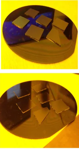
Figure 2.11 Photograph of samples comparing the releasing of microcantilevers with two different techniques which shows the incompatibility and inapplicability of the old technique for processing sophisticated designs.
2.4
Image Gallery: Optical and Scanning Electron Microscopy (SEM)
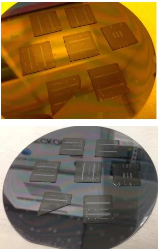
Figure 2.12 Optical image of the top outline showing the single channel microcantilever heaters.
Processed with previous technique
Figure 2.14 Optical image of the top outline showing the micro hotplates.
Experimental Setup and Modeling
3.1
Electrical characterization and sensing setup
For electrical characterization, both Agilent B2902 and Keithley 2612A source
measuring units (SMU) were used. While transmission line matrix (TLM) measurements
were performed using a probe station, regular I-V characterization was performed on
wire-bonded devices.
Sensing setup
Sensing experiments were done in a small chamber, which housed the
wire-bonded sample. The chamber had an inlet and an outlet; wires from the device were taken
out through a small opening near the outlet, which was stuffed with Teflon tape. A
roughing pump along with a valve (V3 in Figure 3.1) was connected to the outlet to
quickly remove the analyte vapor out of the chamber whenever necessary. The inlet side
of the chamber had a mixer assembly – consisting of a mixer junction with valves, a
bubbler and two mass flow controllers. One mass flow controller was used to flow
ultra-high purity (UHP) N2, the other one was used to flow UHP N2 into the bubbler to produce
saturated vapor at room temperature. Both N2 and vapor lines had two valves (V1 and V2,
respectively) connected to them to control the flow of the gas/vapor and eventually
merged into the mixer junction, which directed the vapor mixture into the inlet of the
obtain different concentrations, hence the flow rate of both MFCs were adjusted to get
the desired ratio of N2 and vapor. However, for low concentration (below 200 ppm), the
N2-vapor ratio could become extremely large, creating a backflow of N2 from the mixer
towards the bubbler. In order to avoid that, for such low concentrations, vapor flow rate
was kept 5-20 times higher than its calculated value; but the flow valve V2 was opened
and closed in a pulsed manner to maintain a duty cycle less than 1. The higher flow rate
with lower duty cycle effectively kept the average flow rate very low with reducing the
probability of any backflow. After each sensing experiment, V2 (vapor flow valve) was
closed, but V1 and V3 were kept open. As a result, UHP N2 flushed the chamber while the
pump connected to V3 quickly took out the residual vapor mixture from the chamber.
Figure 3.1 VOC sensing setup.
Sensing Modes for SC-TMH
Sensing characterization for single channel triangular microcantilever heater
(SC-TMH) was done in two different biasing modes. In the first mode (steady-state mode),
applied voltage bias was swept as a staircase function, where a fix dc bias was maintained
for 20-30 s before changing the bias to the next level. During this time, current through
in presence of the analyte vapor. The vapor flow was started right after the first run and
sufficient time (up to 2 min) was given for the vapor concentration to reach the steady
state before the second run was started.
The second mode (transient mode) used the same staircase function, but sampling
frequency was higher (up to 25 Hz) to observe sharp changes in current. Also each step
was of 90-120 seconds duration. Each bias step had three stages – UHP N2 flow to obtain
reference flow, vapor mixture flow to obtain time-resolved response of the device and
finally, again UHP N2 to observe recovery time. Since a single sweep was used to obtain
the reference, sensor response and sensor recovery, second sweep was not necessary.
Sensing Modes for DC-TMH
For dual channel triangular microcantilever heaters (DC-TMH), the inner arm
(channel) was designated as the heater arm (channel) and the outer arm (channel) was
designated as the sensor arm (channel). Only steady-state mode characterization was
done for these devices, as transient response was expected to be of similar nature.
Besides, since the response of DC-TMH comes from a combined contribution of both
channels, time response may not be of great physical significance due to the uncertainty
associated with the contributing factors.
Figure 3.3 Steady-state operating modes of the DC-TMH: (left) Self-heating mode; (right) Secondary heating mode.
For any DC-TMH based sensing experiments, the sensor channel was used as the
transducer. In other words, the response was recorded from the sensor channel only.
modes of steady-state operation (Figure 3.3). In the first mode, namely “self-heating
mode”, the sensor arm is biased at variable dc bias, just like SC-TMH devices. The heater
arm is biased at a fixed low dc bias (~0.5 V), although it does not affect the response of
the sensor channel.
In the second mode, called “secondary heating mode”, the sensor arm is kept at a
fixed low dc bias (~0.5 V) while the heater arm is biased at variable higher dc voltages.
Here the sensor channel does not experience any significant self-heating, but still
becomes hot due to the Joule heating on the heater arm. Therefore, the behavior of the
sensor arm is thermally modulated by the heater arm, making it analogous to a
three-terminal electronic device.
3.2
Thermal characterization setup
The temperature of the micro cantilever heater under a voltage bias was
determined using Raman spectroscopy and infrared thermal microscopy. Raman
spectroscopy was performed to measure the local temperature of the cantilever with
electrical excitation.
Figure 3.5 (a) Raman spectra of the heated cantilever for 300, 400, 500 and 600 K temperature on the hot plate. E2 Peak becomes wider as temperature increases. (b) Shift
in E2 and A1(LO) peaks towards lower wave number as temperature goes up.
Raman characterization setup
In this work a micro-Raman setup by Olympus was used. The sample excitation
utilized a 632 nm HeNe laser while the collection was performed with an 800 cm-1
(a)

![Figure 2.1 (a) Scanning electron microscope (SEM) and (b) infrared (IR) microscope images of the fabricated heated cantilever, indicating heating only near the free end of the cantilever [7]](https://thumb-us.123doks.com/thumbv2/123dok_us/8434105.1388063/31.612.96.520.182.392/scanning-electron-microscope-microscope-fabricated-cantilever-indicating-cantilever.webp)