Current fed DC/DC topology based inverter
S Sai Kumar1, Dr. S.K.Bikshapathy2
1
B.tech scholar, Department of Electrical and Electronics Engineering, Siddhardha Institute of Engineering and Technology, Vinobha Nagar, Ibrahimpatnam, Hyderabad, Telangana-501506
2
Asso.Prof, Department of Electronics and Communication Engineering, Siddhardha Institute of Engineering and Technology, Vinobha Nagar, Ibrahimpatnam, Hyderabad, Telangana-501506
Abstract –
New-age power generation systems based on renewable energy systems (RES) mainly constitute of wind generators, solar PV, fuel cells, etc. Energy harvesting from solar PV or fuel cell calls for high step-up inversion owing to its low-voltage input. Conventional low-voltage source inverter (VSI) can only produce an AC output smaller than its input DC voltage under normal operation. VSI also requires for dead-time compensation circuits as shoot-through of any inverter leg is detrimental for its operation. Recently developed ZSI and its derivatives overcome these problems by allowing shoot-through and providing output AC voltage with buck-boost capability. This paper proposes a CurrentFed DC/DC Topology (CFT) based inverter which shows similar gain characteristic and advantages as the ZSI. The proposed inverter requires only one LC-pair which is one less than the impedance network of ZSI. The proposed inverter is derived from CFT. Steady-state analysis and implementation of the proposed inverter are described. The PWM control strategy of the inverter is explained. An experimental prototype is built to validate the proposed inverter circuit. A 127 V (rms) AC-output is obtained from 353 V DC-link with 35.3 V DC-input and a 5.18 V (rms) ACoutput is obtained from 57.6 V DC-link voltage with 28.8 V DC-input to verify boost and buck mode of operation, respectively.
Index Terms- Current-Fed Switched Inverter, SBI, Shootthrough, EMI.
I. Introduction
In the recent decades the power generation sector has seen large penetration by renewable energy systems (RES) mainly due to rapid depletion of
fossil fuels and technological growth in renewable sector.Renewable sources like solar photovoltaic, fuel cell, etc., are low voltage sources and thus needs high boost inversion to meet the conventional line voltage of 110 V/ 230 V 50/60 Hz AC. Series connection of several sources is another available option but it can cause poor harvest of available energy when solar insolation is locally intermittent (partial shading condition) in the case of solar PV. As AC output of the traditional voltage source inverter (VSI) is always lower than the input DC-link voltage, a front-end DC-DC boost converter or a back-end high step-up transformer is added to get the necessary boost inversion.
extreme duty-cycle operation, but the switching surge voltage due to leakage of the inductors result in associated losses and requirement of high-voltage-rated devices. Use of regenerative snubber or active voltage clamp circuits [6], [7] can prevent production of switch surge and minimize leakage loss but these methods increase circuit complexity and extra loss in the snubber or clamp circuit. Single switch high gain DC/DC converters using four terminal switched cells and switched-capacitor cells are presented in [8]. Though high gain at reduced switch stress is obtained, the number of passive circuit components and diodes are higher than the conventional boost topologies.
One of the major problems associated with the two-stage DC-AC conversion is that the inverter may fail due to electromagnetic noise (EMI). EMI can cause shoot-through of inverter leg leading to flow of short circuit current, and damaging the inverter switches. DC/DC converters which operate at near-unity duty-ratio are more prone to create EMI due to short pulsed current. Thus, conventional VSI needs dead-time compensation circuit. Introducing dead-time in the switching signal introduces waveform distortion which again requires complex dead-time compensation circuitry to nullify the distortion.
In recently developed Z-Source Inverter (ZSI), Quasi-ZSI (q-ZSI) (shown in Fig. 1 (a) and Fig. 1 (b). respectively) and their derivatives, a network of passive elements is sandwiched in between the voltage source (or the DC-link capacitor) and the inverter structure to allow shorting of an inverter leg [9],[10]. Shoot-through state of the inverter enables it to have buck-boost capability and improved EMI noise immunity.
(a) (b)
Fig. 1. Schematic and boost factor of (a) ZSI and, (b) q-ZSI.
ZSI has the disadvantage of having discontinuous input current which is not suitable for fuel cell or photovoltaic application, and hence requires for an input filter stage. Unlike ZSI, q-ZSI possesses continuous input current property as the inductor L1 is placed at the input as shown in Fig. 1(b). The ratio of peak inverter input voltage Vˆpn to the input DC voltage Vg (boost factor) for both ZSI and q-ZSI is
Vˆ pn 1
M ZSI = M qZSI = = (a)
Vg 1-2D
Switched Boost Inverter (SBI) [11] exhibits similar characteristics like ZSI but lowering the passive component count by replacing the “X” shaped impedance network with an active network as shown in Fig. 2. Like ZSI, SBI possesses similar EMI noise immunity. SBI has the minimum number of passive components, i.e., only one inductor and one capacitor. The
drawbacks of SBI are that its boost factor (shown in Fig. 2) is (1-D) times compared to ZSI or q-ZSI which results in smaller gain and it draws
discontinuous input current from DC source.
Fig. 2. Schematic and boost factor of Switched Boost Inverter (SBI).
a) The proposed inverter provides a single-stage DC-to-AC inversion like ZSI, q-ZSI with only one filter-pair.
b) The proposed inverter possesses good EMI noise immunity similar to Z-source derived inverters.
c) It incorporates shoot-through to achieve high boost capability similar to ZSI and q-ZSI.
d) It does not require extreme duty-ratio opeduty-ration to achieve high voltage boost.
e) It does not require dead-band for the switching signals and hence waveform distortion is avoided.
f) The proposed inverter alleviates the discontinuous input current problem of ZSI by virtue of having inductor connected to the input terminal making it suitable for renewable application without the necessity of using input filter.
In the next section, basic current-fed DC/DC topology and its complementary topology are reviewed in details. In Section C, development of Current-Fed Switched Inverter (CFSI) and its steady state characteristics are described [11-13]. The PWM control structure of the proposed converter is detailed in Section D. Section E provides the experimental results for the verification of the proposed inverter
II. REVIEW OF THE CURRENT FED
SWITCHED INVERTER
TOPOLOGY
Fig 3: CFSI topology
Fig 4: Simplified CFSI topology
The current fed switched inverter [14] is shown in Fig. 3. The main components of CFSI are one active switch (S), two diodes (Da, Db), one capacitor (Co) and one inductor (L) and which are connected in between voltage source Vg and the inverter bridge. A low pass LC filer is used at the output of the inverter bridge to filter the switching frequency components in the inverter output voltage.
The CFSI topology inserts the shoot- through state (gating upper and lower switches of a phase leg) in its operation to boost the input voltage Vg to Vc. Therefore, the inverter is able to buck and boost the input voltage to a desired output voltage. Since the shoot-through state is present, reliability of the inverter is improved. Thus, inverter provides efficient single stage dc-ac inversion as well as buck boost power conversion. Similar to ZSI and SBI, inverter input is a switched voltage.
Consider the Fig. 4 for better understanding the operation of the inverter. Here, the H-bridge inverter is represented by a single switch Si and turning on of Si represents the shoot-through state. Initially, the capacitor Co is charged to the voltage Vg and the initial inductor current is zero before switching signals are started [15]. The two operation intervals of
CFSI are
(1) shoot-through interval
(2) non-shoot-through interval
and diodes Da and Db become reverse biased as they are now in parallel with Co. In this interval, source Vg and capacitor Co charge inductor L together. Equivalent circuit of CFSI in D interval is shown in the Fig 5. Equations of inductor voltage and capacitor current in D interval are given in (2) & (3).
(2)
(3)
During non-shoot-through interval (D’ interval), switches S and Si are turned off, which forces diodes Da and Db to turn on. Inductor charges Co and power is delivered to the ac load through the inverter. Here, turning off switch Si denotes the power interval or zero interval of the inverter (turning on of switches S1-S2 or S4-S3). Fig 4 shows the equivalent circuit of CFSI in D’ interval and equations of inductor voltage and capacitor current in D’ interval are given in (4) & (5).
(4)
Fig 5:equivalent circuit of CFSI in D interval
Fig 6: Equivalent circuit of CFSI in (1-D) interval
In steady state equilibrium, using inductor volt-second balance and capacitor charge-volt-second balance, we get
(6)
(7)
From equation (6) it is clear that this topology gives maximum gain at duty cycle close to 0.5. The equation of peak ac output is
(8)
where M is the modulation index of the inverter.
The relation between duty ratio and modulation index is given by
D< 1 – M (9)
So the value of M is depends on the value of D. To avoid this limitation of CFSI, the new topology is proposed in this paper which is named as Improved Current Fed Switched Inverter.
III. IMPROVED CURRENT FED
SWITCHED INVERTER
In order to improve the modulation index value, a combination of switch-diode-capacitor is connected in front of the H- bridge inverter as shown in figure 7. The shoot-through state is avoided and the switch ST is capable of doing the same function of the shoot-through state. Initially, the capacitor Co is charged to the voltage Vg and the initial inductor current is zero before switching signals are started. The two operating intervals of the new topology are
1. D interval
Fig 7:improved current fed switched inverter topology
During D interval, switches S and ST are ON state and D1 and D2 become reverse biased as they are now in parallel with C. In this interval, source Vg and capacitor Co charge inductor L together. In D interval, either S1 & S2 or S3 & S4 are turned on and capacitor C is feeding the load. During (1-D) interval switches S and ST are turned off, which forces diodes D1 and D2 to turn on, and the inductor charges Coand power are delivered to the ac load through the inverter. There is no zero interval is present in the inverter. The gain is same as that of CFSI. The inductor current ripple and capacitor voltage ripple are given by
(10)
(11)
Sine PWM technique is used here for controlling the switches. Fig. 8 shows the generation of the PWM control signals of the proposed inverter. Similar to unipolar sine-triangle PWM, gate signals Gs1 and Gs2 are generated by comparing the sinusoidal modulation signals Vm(t) and −Vm(t) with high-frequency carrier signal Vtri(t). In order to generate the switching signals for the switches S and ST by comparing VST and –VST with Vtri(t). The relation between the VST and D is given by
(12)
Fig 8. Generation of the PWM control signals
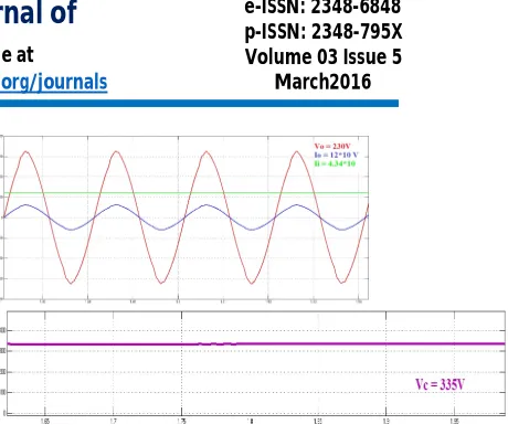
Fig 9: simulation waveforms of output voltage, output current and input current: Fig 10: dc-link voltage Vc
Fig 10: THD and harmonic order of output voltage
IV. SIMULATION RESULTS
fig. 11. The THD content in the output voltage of the proposed inverter is 3.31%.
V. CONCLUSION
Proposed inverter is a single stage high-boost inverter with continuous input which is suitable for the renewable applications. Gain of the inverter is same as that of the ZSI and CFSI. Modulation index of the proposed topology varies from 0 to 1. PWM control strategy is used for the inverter. Simulations results of improved current fed switched inverter are also presented in this paper. Theoretical values are verified by the simulation results.
Reference
[1] Kerekes, T., Liserre, M., Teodorescu, R.,
Klumpner, C., Sumner, M., “Evaluation of
Three-Phase Transformerless Photovoltaic Inverter
Topologies” IEEE Transactions on Power
Electronics, Volume: 24,Issue: 9, 2009, pp. 2202 – 2211.
[2] Gonzalez, R., Gubia, E., Lopez, J., Marroyo, L., “Transformerless Single-Phase Multilevel-Based
Photovoltaic Inverter” IEEE Transactions on
Industrial Electronics, Volume: 55,Issue: 7, 2008, pp. 2694 – 2702.
[3] Carrasco, J.M., Franquelo, L.G., Bialasiewicz,
J.T., Galvan, E., Guisado, R.C.P., Prats, Ma.A.M.,
Leon, J.I., Moreno-Alfonso, N., “
Power-Electronic Systems for the Grid Integration of
Renewable Energy Sources: A Survey” IEEE
Transactions on Industrial Electronics, Volume: 53, Issue: 4, 2006, pp. 1002 – 1016.
[4] Blaabjerg, F., Zhe Chen, Kjaer, S.B., “Power
Electronics as Efficient Interface in Dispersed
Power Generation Systems,” IEEE Transactions
on Power Electronics, Volume: 19, Issue: 5,
2004, pp. 1184 – 1194.
[5] R. W. Erickson and D. Maksimovic,
Fundamentals of Power Electronics, 2nd Edition, Springer science+ business media Inc., NY, 2001.
[6] Rong-Jong Wai, Chung-You Lin, Rou-Yong
Duan, Yung-Ruei Chang, “High-Efficiency DC-DC Converter with High Voltage Gain and
Reduced Switch Stress,” IEEE Transactions on
Industrial Electronics, Volume: 54, Issue: 1, 2007, pp. 354 – 364.
[7] Rong-Jong Wai, Rou-Yong Duan, “High step-up
converter with coupled-inductor,” IEEE
Transactions on Power Electronics, Volume: 20, Issue: 5, 2005, pp. 1025 – 1035.
[8] Ismail, E.H., Al-Saffar, M.A., Sabzali, A.J.,
“High Conversion Ratio DC–DC Converters with
Reduced Switch Stress,” IEEE Transactions on
Circuits and Systems I: Regular Papers, Volume:
55, Issue: 7, 2008, pp. 2139 – 2151.
[9] Fang Zheng Peng, “Z-Source Inverter” IEEE
Transaction on Industrial Applications, Volume. 39, No. 2, 2003, pp. 504-510.
[10] Anderson, J., Peng, F.Z., “Four
Quasi-Z-Source Inverters” in IEEE Power Electronics
Specialists Conference, PESC 2008, pp. 2743 – 2749
[11] Mishra, S., Adda, R., Joshi, A. “Inverse
Watkins–Johnson Topology-Based Inverter”,
IEEE Transactions on Power Electronics,
Volume: 27, Issue: 3, 2012, pp. 1066 – 1070.
[12] J.C. Rosas-Caro, F.Z.Peng, Honnyong Cha, C.
Rogers, “Z-source converter based zero voltage
electronic load,” in IEEE Power Electronics
Specialists Conference, PESC, 2008, pp. 2764 – 2770.
[13] R. Adda, O. Ray, S. Mishra, and A. Joshi,
“Synchronous reference frame based control of switched boost inverter for standalone dc
nanogrid applications,” IEEE Trans. Power
Electron., vol. 28, no. 3, pp. 1219–1233, Mar. 2013.
[14] R. Adda, S. Mishra, and A. Joshi, “Analysis and PWM control of switched boost inverter,” IEEE Trans. Ind. Electron., vol. 60, no. 12, pp. 5593– 5602, Dec. 2013.