Low Power Phase Locked Loop Design with
Minimum Jitter
Krishna B. Makwana, Prof. Naresh Patel
PG Student (VLSI Technology), Dept. of ECE, Vishwakarma Engineering College, Chandkheda, Gujarat, India
Assistant Professor, Dept. of ECE, Vishwakarma Engineering College, Chandkheda, Gujarat, India
ABSTRACT:This paper describes a design of phase locked loop system with low power and minimum jitter. PLLs
with high speed, low noise and wide bandwidth with fast acquistion time are preferred. A PFD with low dead zone, charge pump with passive low pass filter and a low noise, wide tuning VCO are integrated in the PLL system. A Telescopic OTA based VCO with wide tuning range of 450MHz to 1.9GHz and power consumption of 0.30mW is designed.. The PFD modeled is using 15 transistor and conventional charge pump with second order loop filter is used. Integrating this VCO in a PLL system offers low jitter and wide bandwidth. The results prove that maximum pull-in time is 150ns and the power consumed by this PLL system is 606uW at 1.5GHz.Measured jitter is 30ps in this PLL.
KEYWORDS: Phase Locked Loop (PLL), Phase Frequency Detector (PFD), Charge Pump (CP), Loop Filter, Voltage
Controlled Oscillator (VCO), Lock-in range, Lock time, Jitter
I. INTRODUCTION
A PLL is a feedback control system which locks the reference signal to the VCO output signal when the received signal is well within the operating range of the PLL. PLL is used as on chip clock generator, frequency synthesizer and as clock and data recovery system in computer, radio and telecommunication system. A PLL with wide tuning range and low jitter is desired. As the technology scale down, PLL operating at high frequencies are preferred. Conventional voltage phase detector PLLs have many drawbacks like steady state error and limited pull-in range. The design includes a charge pump PLL as it offers zero steady state phase error and infinite pull-in range. It is the VCO which decides the acqusition range of PLL. For a PLL with wide acquisition range a wide tuning VCO is required. In this work, a PLL system is designed with 1GHz operating range. The bandwidth of the PLL is determined by the tuning range of the VCO. But VCO is one of the main sources of jitter. A VCO with high tuning linearity, low noise and wide bandwidth is preferred. ICO offers wide tuning range [1] but the noise at the output is also high. A novel telescopic OTA based ICO with low noise and wide tuning range is designed. This ICO is preceded with a MOS device with current mirrors to make it work as VCO. Active loop filter which is another noise source can be avoided and passive loop filter with conventional charge pump can be used to generate the control voltage. This also reduces the overall system noise and power consumption.
II. LITERATURE REVIEW
consumption. Since jitter is inversely proportional to power consumption the jitter obtained is 65ps and 30ps. [3], [5] operates in MHz with narrow bandwidth and moderate power consumption. These drawbacks can be improved by using a telescopic OTA based ICO which offers wide tuning range, low phase noise and higher design flexibility [4]. The paper comprises of: design of the proposed PLL system in Section 3, section 4 shows the simulation results of the PLL design and performance comparison are made with other PLLs. Section 5 Concludes the paper.
III. PLL DESIGN
The PLL architecture is shown in Fig. 1 and the main components are phase frequency detector, charge pump, loop filter and voltage controlled oscillator.
Figure 1. PLL Architecture
A. Phase Frequency Detector
PFD compares the incoming signal with the PLL output and generate the phase or frequency difference as an error signal. The PFD circuit should consume low power and have a minimum dead zone. Dead zone is a region wherein a PFD fails to detect small frequency/phase errors. This corresponds to one of the sources for jitter. This occurs when there is very small phase difference between the reference signal and VCO output signal. The PFD is designed using 15 transistor and eliminate the reset path. So, power consumption and jitter are reduced in this design.
Figure 2 PFD using 15 transistor[1]
B. Charge Pump
Fig. 3. Charge pump with loop filter
The output control voltage of the charge pump is given by Eqn. 1, Vc(t) is the control voltage, Icpis the output current, Ccp1 is the output capacitance and ∆φ is the phase difference between the two signals.
𝑽𝒄 𝒕 = 𝑰𝒄𝒑
𝟐𝝅𝑪𝒄𝒑𝒕∆φ Eq…(1)
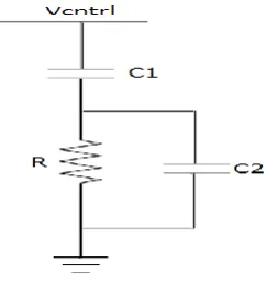
C. Loop Filter
Loop filter eliminates the undesirable high frequency components and retain the dc level of the generated control voltage(Vcntrl). It also determines the stability of the system. Active loop filters offer wide output swing at the cost of increased device noise and high power consumption. A passive second order RC filter shown in Fig. 4 is used. The resistance in series to output capacitance C1 adds a zero to the transfer function to improve the stability of the system. A capacitance C2 is added in parallel to the resistance to control the ringing of the output voltage at high frequencies.
Figure 4 Loop Filter
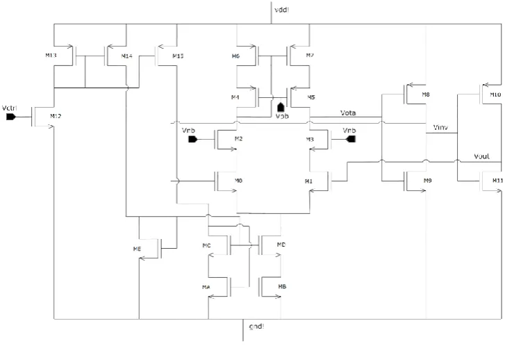
D. Telescopic OTA Based VCO
1) OTA Stage: The circuit diagram of single ended telescopic OTA is shown in Fig. 5. The NMOS transistors M0, M1 forms the input differential pair. M2 and M3 is the cascode device of the input pair. They are biased to be in saturation for this current range.PMOS transistors M4 to M7 forms the single ended cascade current mirror load. The devices are sized to handle this current swing and reduce the overdrive voltage so that the output swing of the OTA is well enough to trigger the oscillations.
Fig 5. Telescopic OTA[4]
2) Biasing Current Mirrors: The circuit diagram of high swing cascode current mirrors is shown in Fig. 6. The NMOS transistors MA-MD forms the high compliance cascode current mirrors to bias the OTA with the control current from the preceding stage. ME is a diode connected transistor which sets VGS for MC and MD so that they are in saturation for different values of Ictrl.
3) Inverter Stages: The circuit diagram of output stage with two inverters cascaded is shown in Fig. 7. The size of these inverters is kept minimum which improves the speed and reduces the chip area. CMOS transistors M8, M9 and M10,
M11 are identical.
Fig 6. Baising Circuit[4] Fig 7. Inverter stage[4]
To integrate this ICO in PLL system a V to I Converter stage should be preceded. A simple MOS device when operated in saturation region produces a current proportional to the input voltage. This change in drain current with respect to change in input votage is called transconductance. A device with high transconductance converts small voltage change to large output current,which induces high frequency of oscillation in the designed ICO. The electrical representation of the proposed VCO block is shown in Fig. 6.
The electrical representation of the block VCO is shown below.
Fig 8 Telescopic OTA Based VCO[4]
IV. SIMULATION RESULT
The output clock generated for a frequency of 200 MHz is shown in Fig. 9. The time taken for the PLL to lock to the reference frequency is 150ns. The control voltage for this frequency is 640mV and is stable in the acqusition period. The jitter measured is 30ps for 200MHz.
The PLL output and the reference signal under locked state are shown in Fig. 10. The jitter measured is 30ps for 200MHz.
Fig. 10. Reference signal in black and VCO signal in red under locked state
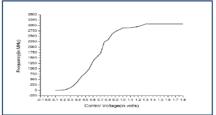
The VCO tuning characteristics is plotted in Fig. 11. The use of ICO improved the tuning linearity and the high figure of merit of the MOS device used for V to I conversion enhances a tuning range 450MHz to 2GHz for low control voltage range of 400mV to 750mV.
Fig.11 Tuning characteristics of Voltage controlled oscillator
The average power consumption at 200MHz freq is 606uW and measured jitter is 30ps in the designed PLL.
The measured results of the proposed design and the comparison with other works is tabulated in Table I.
Table I Performance Comparision of PLL
Parameters Proposed Work [4] [3] [6]
Nominal Frequency (MHz) 1500 1000 720 270
Operating Frequency (MHz) 450-1900 500-1500 640-800 100-500
Power Supply (v) 1.8 1.8 1.8 1.8 Technology (um) 0.18 0.18 0.18 0.18
Jitter (ps) 30 24 30 32 Average Power Consumption
(mW)
V. CONCLUSION
In phased locked loop system, The average power consumption in 15 transistor PFD is 26uW which is less than the Conventional PFD and jitter is also minimized in PFD design by removing the reset path . Telescopic OTA Based VCO has wide tuning range of 450MHz to 1.9GHz and average Power Consumption of 0.3mW at 1200MHz Frequency. The Total Average Power Consumption in PLL System is 0.606mW at Input Frequency 150MHz and measured Jitter is 30ps.
REFERENCES
[1] Abdul Majeed K.K. and Binsu J Kailath, “Low power, High Frequency, Free Dead Zone PFD for a PLL Design”, Indian Institute of Information Technology Design and Manufacturing(IIITD&M) Kancheepuram, Chennai, India..IEEE 2013
[2] Herv Barthlemy, Stphane Meillre and Sylvain Bourdel, “ Single ended rail to rail CMOS OTA based variable frequency ring oscillator”,IEEE ISCAS,Vol 4, Page(s): 537-40, 2004
[3] Gauri Shankar Singh, Devesh Singh, S.Moorthi,” Low Power Low Jitter Phase Locked Loop for High Speed Clock Generatio. Asia Pacific Conference on Postgraduate Research in Microelectronics & Electronics (PRIMEASIA), Page(s):192 – 196, ISSN : 2159-2144, December 2012.
[4] S. Aditya_ and S. Moorthi_.”A Low Jitter Wide Tuning range Phase Locked Loop with Low Power Consumption in 180nm CMOS Technology” Asia Pacific Conference on Postgraduate Research in Microelectronics & Electronics (PRIMEASIA),IEEE, Pages:- 228 – 232, 2013
[5] Behzad Razavi, Design of Analog CMOS Integrated Circuits, International Edition, McGraw Hill publications, 2001.
[6] S. Willium_ and H. Thompson_.”An Improved CMOS Ring Oscillator PLL With less than 4ps accumulated jitter”,IEEE preceeding of CICC04, Sep 2004
BIOGRAPHY
Makwana Krishna is PG student in EC Department, College of Vishwakarma Engineering College,Chandkheda,
Gujarat Technological University. She is doing master in Signal Processing and VLSI Technology. Her Research interest is low power VLSI circuit design.
Naresh Patel is Assistant Professor in EC Department, College of Vishwakarma Engineering College, Chandkheda,
![Fig 5. Telescopic OTA[4]](https://thumb-us.123doks.com/thumbv2/123dok_us/1486828.1181907/4.595.233.385.241.408/fig-telescopic-ota.webp)