ISSN(Online) : 2319-8753
ISSN (Print) : 2347-6710
I
nternational
J
ournal of
I
nnovative
R
esearch in
S
cience,
E
ngineering and
T
echnology
(An ISO 3297: 2007 Certified Organization)
Vol. 4, Special Issue 13, December 2015
Area Efficient Multiband Frequency Divider
C.Jagadeeshwaran
1,A.Muthukumar
1Assistant Professor,Dept. of ECE, Sasurie College of Engineering, Tirupur, Tamilnadu, India1
ABSTRACT:In this paper the prescaler circuit which is used by frequency synthesizers of Bluetooth, zigbee and WLAN is proposed with multi modulus 32/33/47/48 prescaler, New E-TSPC 2/3 prescaler, P-counter and S-counter. This proposed prescaler can divide the frequency in three bands 0f 2.4-2.484GHz, 5.15-5.35GHz and 5.725-5.825GHz with a resolution selectable from 1-25MHz.The Area and power consumed by the multimodulusprescaler circuit is minimized.
KEYWORDS:DFF, frequency synthesizer, E-TSPC, wireless LAN (WLAN), true single phase clock (TSPC)
1. INTRODUCTION
Wireless LAN (WLAN) in the multigigahertz bands, such as HiperLAN II and IEEE 802.11a/b/g, are the leading standards for high-rate data transmissions, and standards like IEEE 802.15.4 are recognized for low-rate data transmissions. The demand for lower cost, lower power, and multiband RF circuits increased in conjunction with need of higher level of integration. The frequency synthesizer, usually implemented by a phase-locked loop (PLL) is one of the power-hungry blocks in the RF front-end, and the first-stage frequency divider consumes a large portion of power in a frequency synthesizer.The integrated synthesizers for WLAN applications at 5GHz reported in [3] consume up to 25mW in CMOS realizations.
The frequency synthesizer reported in [4] uses an E-TSPC prescaler as the first-stage divider, but the divider consumes around 6.25mW. A low-power clock multiband divider for Bluetooth, Zigbee, and IEEE 802.15.4 and 802.11 a/b/g WLAN frequency synthesizers based on pulse-swallow topology is reported in [1], and it is implemented using a 0.18µm CMOS technology. The multiband divider consists of a wide band multimodulus 32/33/47/48 prescaler and swallow (S) counter and p-counter. In this proposed system the TSPC 2/3 prescaler in [1] is replaced by the New E-TSPC 2/3 prescaler[2], which consumes low power and area when compared to the existing design.
II. BLOCK DIAGRAM
ISSN(Online) : 2319-8753
ISSN (Print) : 2347-6710
I
nternational
J
ournal of
I
nnovative
R
esearch in
S
cience,
E
ngineering and
T
echnology
(An ISO 3297: 2007 Certified Organization)
Vol. 4, Special Issue 13, December 2015
Fig.1. Multiband Divider Block
Fig.2. Proposed Multi-Modulus 32/33/47/48 Prescaler
III. NEW E-TSPC 2/3 PRESCALER
This New low power E-TSPC 2/3 prescaler is introduced from [2] which is shown in Fig.3, and this is the further improved version of the Existing prescaler.It consist of two flipflops and the and gate as like previous design. The OR gate used for the divide control is replaced with a PMOS transistor, it act likes a switch. Note that there is a negation bubble at one of the AND gate‟s input. The output Q of FF1 is thus complemented before being fed to FF2. When the switch is open, the input from FF1 is disconnected and FF2 alone divides the clock frequency by 2. When the switch is close, FF1 and FF2 are linked to form a counter with three distinct states. Besides the speed advantage, E-TSPC FFs are particularly useful for low voltage operations because of the minimum height in transistor stacking.
ISSN(Online) : 2319-8753
ISSN (Print) : 2347-6710
I
nternational
J
ournal of
I
nnovative
R
esearch in
S
cience,
E
ngineering and
T
echnology
(An ISO 3297: 2007 Certified Organization)
Vol. 4, Special Issue 13, December 2015
Other than the two E-TSPC FFs, only one pMOS Transistor (PMC) is needed. The pMOS transistor controlled by the
divide control signal serves as the switch. The AND gate plus its input inverter are achieved by way of wired-AND logic using no extra transistors at all. The proposed design scheme is far more sophisticated than the measure of simply adding one pass transistor may suggest. First of all, unlike any previous designs, the E-TSPC FF design remains intact without any logic embedding. Both speed and power behaviors are not affected, which indicates a performance edge over the logic embedded FF design. Secondly, the inverter to complement the one of the two E-TSPC FF outputs for divide-by-3 operations is removed in the proposed design. The circuit simplification, again, suggests the improvements in both speed and power performances.
IV. 32/33/47/48 PRESCALER
The proposed wide band multimodulusprescaler is shown in Fig.4, which can divide the input frequency by 32, 33, 47, and 48. It is similar to the 32/33 prescaler. But it consists of additional inverter and a multiplexer as like existing design. This prescaler performs additional divisions (divide- by-47 and divide-by-48) without any extra flip-flop, thus saving a considerable amount of power and also reducing the complexity of multiband divider which will be discussed below. The multimodulusprescaler consists of New E-TSPC 2/3 prescaler [2], four divide-by-2 circuits ((AD)=16) and combinational logic circuits for getting multiple division ratios. Beside the usual MOD signal for controlling N/(N+1)) divisions, the additional control signal Sel is used to switch the prescaler between 32/33 and 47/48 modes.
Fig.4.Multimodulus 32/33/47/48 PrescalerUsing New E-Tspc 2/3 Prescaler
a. CASE 1: Sel= ‘0’
When Sel = „0‟ , the output from the NAND2 gate is directly transferred to the input of 2/3 prescaler and the multimodulusprescaler operates as the normal 32/33 prescaler, where the division ratio is controlled by the logic signal MOD. If MC=„1‟, the 2/3 prescaler operates in the divide-by-2 mode and when MC=‟0‟, the 2/3 prescaler operates in the divide-by-3 mode. If MOD = „1‟, the NAND2 gate output switches to logic “1” (MC = „1‟) and the wide band prescaler operates in the divide- by-2 mode for entire operation. The division ratio N of the multimodulusprescaler is
N= (AD*N1) + (0* (N1 + 1)) = 32. (1)
Where N1 = „2‟ and AD = „16‟ is fixed for the entire design. If MOD = „0‟ , for 30 input clock cycles „MC‟ remains at
logic “1”, where wideband prescaler operates in divide-by-2 mode and, for three input clock cycles, „MC‟ remains at logic “0” where the wideband prescaler operates in the divide-by-3 mode. The division ratio N+1 of themultimodulusprescaler is
N+1 = ((AD - 1) * N1) + (1 * (N1 +1)) = 33. (2) 4.2 CASE 2: Sel = ‘1’
When Sel = „1‟, the inverted output of the NAND2 gate is directly send to the input of 2/3 prescaler and the multimodulusprescaler operates as a 47/48 prescaler, and the division ratio is controlled by the signal „MOD‟. If MC=„1‟, the 2/3 prescaler operates in divide-by-3 mode and when MC=„0‟, the 2/3 prescaler operates in divide-by-2 mode‟. If MOD=„1‟, the division ratio N +1 performed by the multimodulusprescaler is same as (1) except that the wide band prescaler operates in the divide-by-3 mode for the entire operation given by
N +1 = (AD * (N1 + 1)) + (0 * N1) = 48 (3)
If MOD = „1‟, the division ratio N performed by the multimodulusprescaler is
ISSN(Online) : 2319-8753
ISSN (Print) : 2347-6710
I
nternational
J
ournal of
I
nnovative
R
esearch in
S
cience,
E
ngineering and
T
echnology
(An ISO 3297: 2007 Certified Organization)
Vol. 4, Special Issue 13, December 2015
V. MULTIBAND FLEXIBLE DIVIDER
The single-phase clock multiband flexible divider which is shown in Fig.1, consists of the Proposed multimodulus 32/33/47/48 prescaler, a 7-bit programmable P-counter and a 6-bit swallow S-counter. The multimodulus 32/33/47/48 precaler is briefly discussed in Section IV. The control signal Sel decides whether the divider is operating in lower frequency band or higher band. The operation of P-counter and S-counter are same as the existing system[1]
VI. SIMULATIONS
The proposed multimodulusprescaler has the maximum operating frequency of 7.2 GHz (simulation)[1]. The simulation results of this proposedmultimodulusprescaler in different mode of operation (32/33/47/48) is shown in the Fig.7. These simulation waveforms are carried out by using Modelsim6.4c(Verification tool)
(a)
(b)
ISSN(Online) : 2319-8753
ISSN (Print) : 2347-6710
I
nternational
J
ournal of
I
nnovative
R
esearch in
S
cience,
E
ngineering and
T
echnology
(An ISO 3297: 2007 Certified Organization)
Vol. 4, Special Issue 13, December 2015
(d)
Fig.7. Simulation Result of MultimodolusPrescaler during (a)divide by 32 mode, (b) divide by 33 mode, (C) divide by 47 mode, (d) divide by 48 mode.
The simulation waveform of the entire divider block including P& S counter and “FD” for some clock cycles is shown in the Fig. 8.
Fig.8. Simulation Waveform of Multiband Divider
ISSN(Online) : 2319-8753
ISSN (Print) : 2347-6710
I
nternational
J
ournal of
I
nnovative
R
esearch in
S
cience,
E
ngineering and
T
echnology
(An ISO 3297: 2007 Certified Organization)
Vol. 4, Special Issue 13, December 2015
(a)
(b)
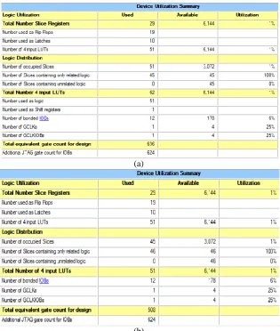
Fig.9. (a) Area Utilization of Existing Design, (b) Area Utilization of Proposed Design. Table 1 Result Comparison.
Logic Utilization In This Paper Existing Design [1]
Total No. of Slice Registers 29 29
No. of Occupied Slice 45 51
Total No. of 4 Input LUTs 51 62
ISSN(Online) : 2319-8753
ISSN (Print) : 2347-6710
I
nternational
J
ournal of
I
nnovative
R
esearch in
S
cience,
E
ngineering and
T
echnology
(An ISO 3297: 2007 Certified Organization)
Vol. 4, Special Issue 13, December 2015
Fig.10. Comparison chart
VII. CONCLUSION
In this paper, New E-TSPC 2/3 prescaler is used in wide band multimodulus 32/33/47/48 prescaler. A dynamic logic multiband flexible integer-N divider is designed which uses E-TSPC 2/3 prescaler [2]. The P-counter and S-counter values are programmable and it is programmed to the divider between the range of 1 to 6.2 GHz with finest resolution of 1 MHz and variable channel spacing. since interest lies in the 2.4- and 5–5.825-GHz bands of operation, the P- and S-counters are programmed accordingly. The proposed multiband flexible divider also uses an improved loadable bit-cell for P & S counters. The overall equivalent gate count of the design is reduced to 508 from 636.
REFERENCES
[1] Vamshi Krishna Manthena, ManhAnh Do, ChirnChye Boon, and KiatSeng Yeo, “A Low-Power Single- Phase Clock Multiband Flexible Divide,r” IEEE Transactions On Very Large Scale Integration (VlSI) Systems, Vol. 20, No. 2, February 2012
[2] Yin-Tsung Hwang and Jin-Fa Lin “Low Voltage and Low Power Divide-By-2/3 Counter Design Using Pass Transistor Logic Circuit Technique” IEEE Transactions On Very Large Scale Integration (VLSI) Systems, Vol. 20, No. 9, September 2012
[3] H.R.Rateghet al., “A CMOS frequency synthesizer with an injectedlocked frequency divider for 5-GHz wirless LAN receiver,” IEEE J.Solid-State Circuits, vol. 35, no. 5, pp. 780–787, May 2000.
[4] S. Pelleranoet al., “A 13.5-mW 5 GHz frequency synthesizer with dynamic-logic frequency divider,” IEEE J. Solid-State Circuits, vol. 39, no. 2, pp. 378–383, Feb. 2004.
[5] X. P. Yu et al., “Design of a low power wideband high resolution programmable frequency divider,” IEEE Trans. Very Large Scale Integr. (VLSI) Syst., vol. 13, no. 9, pp. 1098–1103, Sep. 2005.
0 100 200 300 400 500 600 700
Total No. of Slice Registers
No. of Occupied Slice
Total No. of 4 Input LUTs
Total Equivalent Gate Count
In This Paper