Analysis of PCB to find Trace Impedance by
Method of Moment and Cross-talk Interference
Avali Ghosh1, Sisir Kumar Das2, Annapurna Das3
1. ,2, 3
ECE Department, MAKAUT, GNIT, Kolkata
Abstract: In this paper the impedance of PCB trace is calculated from the charge distribution on microstrip line using method of moment. The parasitic element values are computed to find the crosstalk interference in PCB. The results of theoretical analysis are obtained by using MATLAB. The crosstalk interference also found using modeling and simulation with Ansoft HFSS tool. These results are compared with the experimental results and found good agreement.
Keywords: Crosstalk, Multi-conductor PCB traces, Near - end crosstalk, Far - end crosstalk, Method of Moment.
I. INTRODUCTION
Double layer printed circuit board consists of multi-conductor microstrip traces. In dense PCB designs, crosstalk interference occurs due to electromagnetic coupling between signal traces through mutual inductances and mutual capacitances. Several authors analyses coss-talk in PCB[1-10]. In this paper the line parameters such as capacitances and characteristic impedance are calculated from the charge distribution on the trace by method of moment. The parasitic element values are computed to find the crosstalk interference in PCB. The crosstalk interference also found using modeling and simulation with Ansoft HFSS tool. These results are compared with the experimental results and found good agreement.
II. LINEIMPEDANCEUSINGMETHODOFMOMENT
In high-speed systems, control of the electrical characteristics of the transmission lines is crucial. The basic electrical characteristics that define a transmission line are its characteristic impedance and its propagation velocity. In this analysis the PCB traces of equal
width w above a FR-4 dielectric substrate of thickness h and dielectric constant
r
4
.
4
are considered above a ground plane. The line impedance of the trace can be obtained using empirical formula [11]. These formulae was derived using some assumptions and depend on trace width/substrate thickness. The traces are designed in this paper very accurately for 50 ohm using Method of Moment as described belowA. MOM Segmentation
For surface charge distribution, the microstrip section is divided into N sections as shown in Fig. 1.
n
1
,
2
,
3
,...
,
M
on the strip (1a)n
M
1
,
M
2
,
M
3
,....,
N
on the ground plane (1b)Fig. 1 Cross-sectional view of Microstrip section
Charge density
is constant on each segment
S
n
N n
n n
f
1
where
f
n
1
on
S
n
0
elsewhere
n
constant coefficient corresponding to
S
n
charge per unit length and unit width of element
S
nThe characteristic impedance of the line is
C
Z
1
0
(2a)where
Velocity of wave inside the hybrid mediumC
Capacitance of the line / length0 0 0 1
)
,
(
V
f
V
Q
V
ds
y
x
C
S
n n
(3)The charge distribution on the strip
(
x
,
y
)
is determined by method of moment using Poisson's equation:r
V
0 2
(4)Therefore electric potential inside the substrate between strips and ground plane is
2 1,
(
1
)
,
(
0 r S S
y
x
G
y
x
V
x
,
y
)
(
x
,
y
)
d
s
(5) Since
0
in the substrate betweenS
1andS
2, integration is performed are the strip and ground surfaces.y
x
G
(
,
r
s
d
y
x
e
y
x
4
1
)
,
(
)
,
is the Green's function for the line.)
,
(
x
y
V
satisfies boundary conditions0
)
,
(
x
y
V
on the ground plane aty
0
(6a)
V
0 on the strip aty
h
(6b) Substituting equation 2 to equation 5
S N n ry
x
G
y
x
V
(
,
)
1
(
,
1 0
s
d
f
y
x
,
)
n n
(7)
For unit pulse function
f
n
1
on
S
n
0
elsewhere Equation 7 reduces to
n S m m N n n n n r mm
y
x
y
G
x
y
x
V
(
,
)
1
,
(
,
1 0
x
n,
y
n)
nf
ndS
n (8)
m m
y
x
,
observation point on the conductor
n n
y
x
,
source point on the conductor
mn
nr
G
V
01
(9)Therefore unknown coefficients can be determined
n r
G
mn
V
1 0
(10) whereV
V
0forn
1
,
2
,
3
,...
,
M
0
forn
M
1
,...,
N
)
,
(
m
n
the element
n S m m mnG
x
y
G
(
,
x
n,
y
n)
dS
n(11)
Capacitance is expressed in terms of total charge on one of the conductors,
0 1
V
S
C
M n n n
(12)The line impedance is computed using eqns. 2a and 12.
B. Line Parasitic elements and Crosstalk
The derived empirical equations on the electrical parameters of the microstrip line in the inhomogeneous medium with one side exposed to air are as follows [5]:-
36 . 1 25 . 0 049 . 0 963 . 07
.
2
75
.
0
*
*
52
.
3
exp
07
.
1
15
.
1
h
t
h
w
h
s
h
t
h
w
C
t
(13)
0.78 0.8 0.037 0.98 083 . 0
227
.
0
36
.
1
*
32
.
1
402
.
0
*
17
.
1
h
t
h
w
h
s
h
s
h
w
C
m
(14)
0.73 0.0006 0.0052 0.026 041 . 0
84
.
0
75
.
0
*
*
89
.
1
exp
39
.
3
018
.
0
71
.
3
t
h
w
h
h
s
t
h
w
h
w
h
L
O S
(15)
0.16 1.18 2.6 2.03 0.13 1.09
37
.
1
418
.
0
*
89
.
0
07
.
1
*
*
38
.
2
415
.
0
w
t
w
h
h
s
h
s
w
t
w
h
L
O m
(16)Crosstalk due to electromagnetic coupling between signal traces through mutual inductance and stray/mutual capacitance between two or more conducting traces or interconnect can be expressed as follows [6]
L S L fe ne fe ne L S fe ne ne S neR
R
C
R
R
R
R
R
R
R
L
R
R
R
j
V
V
12 12*
*
(17)
L S L fe ne fe ne L S fe ne fe S neR
R
C
R
R
R
R
R
R
R
L
R
R
R
j
V
V
12 12*
*
III.RESULTSANDDISCUSSION
A. Theoretical Result
Self capacitance has been calculated with the method of moment to design the PCB for 50 ohm trace impedance. The results for charge distribution on the trace and impedance versus w/h are shown Fig. 2.
Fig. 2 a) Charge distribution Vs Width of the trace by using MOM
b)
Z
0Vsw
/
h
1
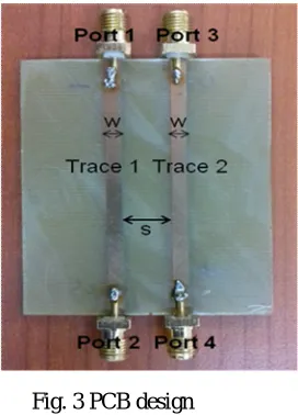
of microstrip line [image:5.612.59.557.137.334.2]In this PCB design two parallel traces of 50 ohm are on the top surface above the dielectric substrate and copper plane is at the bottom is considered as shown in Fig. 3. A PCB was made with FR4 material, height of substrate, h = 1.6mm. The thickness of the copper trace t is assumed negligible i.e. t = 0.001mm and trace width w = 3.1mm, spacing between two traces is s = 6.2mm.
Fig. 3 PCB design
The mutual inductance and capacitance between two conducting traces are computed by using empirical formulae equation 14 and equation 16. Self capacitance and inductance has been calculated with the method of moment.
-09
10
3.3520
t
L
H/m-09
10
1.1238
m
L
H/m-12
10
.1261
1
t
[image:5.612.255.391.425.614.2]-12
10
.6402
1
m
C
F/mCrosstalk due to near-field / reactive field electromagnetic coupling between two conducting traces at 1GHz are
dB
V
next
29
.
6758
dB
V
fext
34
.
5617
Self capacitance and inductance has been calculated with the method of moment. The mutual inductance and capacitance between three conducting traces computed are
-09
10
4.5503
t
L
H/m-09
10
18806
.
8
m
L
H/m-12
10
1.0379
t
C
F/m-12
10
.9006
1
m
C
F/mCrosstalk due to near-field / reactive field electromagnetic coupling between three conducting traces at 1GHz are
dB
V
next
7
.
8186
dB
V
fext
19
.
3347
B. Experimental Result
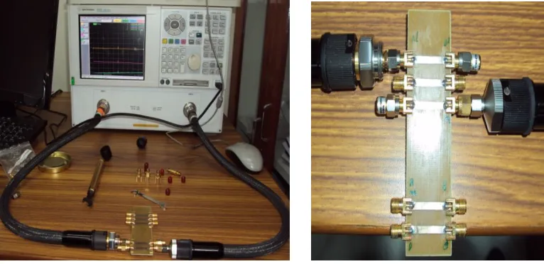
The experimental measurement of crosstalk is done by using Agilent PNA Series Network Analyzer E8363B (10 MHz – 40 GHz) in SAMEER, Kolkata. The coupling parameters S31 (Near-end) and S41 (Far-end) are measured. The experimental setup with network analyser are shown in Fig. 4.
[image:6.612.120.503.449.635.2]
Fig. 4 Experimental setup with network analyser
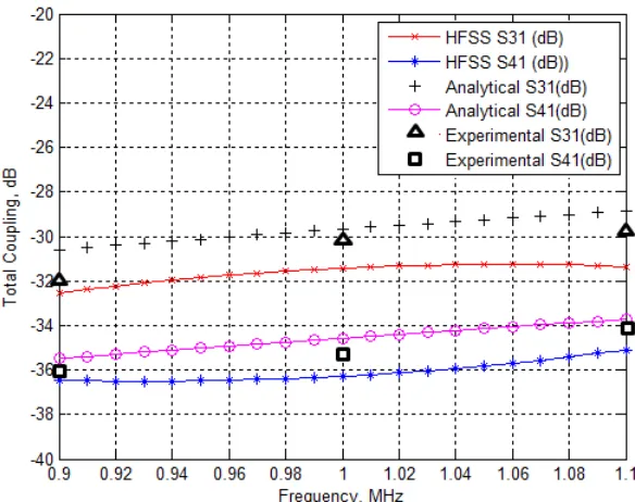
Fig. 5 Crosstalk Vs Frequency for Two adjacent traces ( w=3.1mm, s=6.2mm, h=1.6mm, εr=4.4)
Fig. 6 Crosstalk Vs Frequency for Three adjacent traces ( w=3.1mm,s=6.2mm, h=1.6mm, εr=4.4)
The discrepancies observed in these results are due to various assumptions made in the theory and also due to non ideal situations in the experimental setups.
IV.CONCLUSIONS
good agreement with little discrepancies due to various assumptions made in the theory and also due to non ideal situations in the experimental setups.
REFERENCES
[1] Paul C. R., Introduction to Electromagnetic Compatibility , A Wiley- Interscience Publications, John Wiley & Sons, Inc, Newyork, 1987. [2] Paul C. R., Analysis of Multi Conductor Transmission Lines, A Wiley- Interscience Publications, John Wiley & Sons, Inc, Newyork,, 1984. [3] R.F. Harrington, Method of Moment, Wiley Publication.
[4] R. F. Harrington, Time - Harmonic Electromagnetic Fields, Donald G. Dudley, Series Editor, Wiley Publication.
[5] Young-Soo Sohn, Jeong-Cheol Lee, Hong-June Park and Soo-In Cho , ‘ Empirical Equations on Electrical Parameters of Coupled Microstrip Lines for Crosstalk Estimation in Printed Circuit Board’ , IEEE Transactions on Advanced Packaging, VOL. 24, NO. 4, November 2001.
[6] Stephen H. Hall and Howard L. Heck, Advanced Signal Integrity for high speed digital designs, A Wiley- Interscience Publications, John Wiley & Sons, Inc, USA, 2000.
[7] Charles Walker, Capacitance, Inductance and Crosstalk Analysis, Artech House, 1988.
[8] Grover. F. W., Inductance Calculations, Working Formulas and Tables, Drover Publications, Newyork, 1946.
[9] Paul C. R., Computation of Crosstalk in Multiconductor Transmission Lines’ , IEEE Transactions on EMC, VOL EMC-23, No-4, 1981.
[10] Clayton R. Paul, ‘Solution of the Transmission-Line Equations Under the Weak-Coupling Assumption’, IEEE Transactions on Electromagnetic Compatibility, VOL. 44, NO. 3, August 2002.