N A N O E X P R E S S
Open Access
Improvement of performance of InAs quantum
dot solar cell by inserting thin AlAs layers
Dongzhi Hu
1*, Claiborne CO McPheeters
2, Edward T Yu
2, Daniel M Schaadt
1Abstract
A new measure to enhance the performance of InAs quantum dot solar cell is proposed and measured. One monolayer AlAs is deposited on top of InAs quantum dots (QDs) in multistack solar cells. The devices were fabricated by molecular beam epitaxy.In situannealing was intended to tune the QD density. A set of four samples were compared: InAs QDs withoutin situ annealing with and without AlAs cap layer and InAs QDsin situ annealed with and without AlAs cap layer. Atomic force microscopy measurements show that whenin situ annealing of QDs without AlAs capping layers is investigated, holes and dashes are present on the device surface, while capping with one monolayer AlAs improves the device surface. On unannealed samples, capping the QDs with one monolayer of AlAs improves the spectral response, the open-circuit voltage and the fill factor. On annealed samples, capping has little effect on the spectral response but reduces the short-circuit current, while increasing the open-circuit voltage, the fill factor and power conversion efficiency.
Introduction
Group III-V compound semiconductor solar cells are the highest efficiency cells developed to date [1] due to the wide range of bandgaps that can be grown with high crystalline quality in this material system. Record effi-ciencies around 40% [2] are achieved in triple junction cells with an InGaP/InGaAs/Ge structure, in which lat-tice-matched InGaAs replaces a middle GaAs layer. Due to the three-dimensional confinement of quantum dots (QDs), their incorporation into the middle layer enhances the photo current of solar cells, which can be further improved by forward scattering techniques [3]. The elec-tronic properties of QDs depend on their size, shape, and surrounding matrix [4] and can be tuned during molecu-lar beam epitaxy (MBE) by growth rate, temperature, and in situannealing procedures [5,6]. In particular, it is pos-sible to tailor the absorption spectrum of the InAs QDs to the 1.0 to 1.2 eV range, which allows for enhanced absorption with respect to the solar spectrum. To tailor
the absorption spectrum of the InAs QD, an in situ
annealing procedure is often used. Annealing of InAs QDs at relatively low temperatures, i.e., lower than 470°C right after their deposition leads to classical Ostwald
ripening. In this case, the dot density decreases with smaller dots disappearing while larger dots growing with annealing time. When the dot size becomes larger than a critical value, dislocations are formed, which is not pre-ferred for solar cells. However, when annealing InAs QDs at relatively high temperatures, i.e., higher than 490°C, a combination of ripening and InAs decomposi-tion occurs. The size and chemical composidecomposi-tion of QDs can then be tuned without formation of defects [7]. For enhancement of absorption, vertical stacks of InAs QDs embedded in InGaAs/GaAs are preferred, where segrega-tion of In has to be considered, especially with anin situ annealing procedure [8]. To suppress this In segregation, a thin AlAs capping layer can be introduced [9,10]. How-ever, the effect of this thin AlAs layer on the device performance is thus unclear and needs to be studied.
In this study, we fabricated GaAs-basedp-i-njunctions with a stack of 10 layers of InAs QDs as the intrinsic layer. The density of the InAs QDs in each layer was tuned byin situannealing at high temperature. To sup-press In segregation and thereby keeping the InAs QD composition approximately constant, one monolayer AlAs was deposited on top of the QD layer. The influ-ence of capping the dots with a monolayer of AlAs
on devices with and without in situannealed QDs is
investigated. * Correspondence: [email protected]
1
Institut für Angewandte Physik/DFG-Center for Functional Nanostructures, Karlsruhe Institute of Technology (KIT), Karlsruhe, Germany
Full list of author information is available at the end of the article
Experimental
The solar cell structures are shown in Table 1. Before growth of the structures, epi-ready Si-doped GaAs (100) substrates were pre-degassed in a load lock chamber at 130°C for 1 h. Then the substrates were transferred into the growth chamber and heated up to 600°C under As4
ambient conditions to remove the oxide layer. In situ reflection high energy electron diffraction (RHEED) was used to observe the surface reconstructions. When a clear 2 × 4 reconstruction appeared, we decreased the temperature to 570°C to start growth of a 1μm thick n-doped GaAs with a doping level of 7 × 1018cm-3. Then 10 stacks of 20 nm intrinsic GaAs, covered by InAs QDs capped with a 6.6 nm thin In0.12Ga0.88As layer,
were deposited. For the InAs QDs layers, we deposited nominally 2.3 monolayers, which correspond to 0.69 nm thick. Since the InAs QDs are formed in the Stranski-Krastanov growth mode, this leads to a wetting layer of about 1.6 monolayer thickness and the QDs on top of it. For devices with in situannealed QDs, the growth was interrupted right after deposition of each of the InAs QDs for 5 min. The temperature was kept at the growth temperature, thereby allowing for In surface dif-fusion and desorption, resulting in a combined rearran-gement of the InAs QDs to a distribution with lower dot density and lower In content [7]. For devices with AlAs capping, one monolayer (0.283 nm) of AlAs was deposited on top of the QDs before covering them with the 6.6 nm thick In0.12Ga0.88As layer. At the end a
20 nm thick intrinsic GaAs layer followed by a 100 nm thick p-doped GaAs of 1 × 1019cm-3 was deposited. Sili-con and Beryllium were used as n- and p-type dopants.
During growth, the equivalent beam pressure of As4
remained at 3.0 × 10⁻⁶Torr and equivalent beam pres-sure of Ga, In, and Al were 4.67 × 10⁻⁷Torr, 2.0 × 10⁻⁸ Torr, and 1.2 × 10⁻⁸Torr, respectively. The temperature was calibrated by a pyrometer. The growth rates were calibrated by RHEED specular spot oscillations. In total, we fabricated four types of samples: sample A contains unannealed QDs without AlAs capping. Sample B
contains unannealed QDs with AlAs capping. Samples C and D contain annealed QDs without and with AlAs capping, respectively. In order to distinguish the differ-ence of these four types of samples, they are summar-ized in Table 2. The morphology of the device surface was measured by atomic force microscopy (AFM) in contact mode. Devices were illuminated with a Newport Oriel 96000 solar simulator operating at 160 W while device performance was measured with a Hewlett-Packard 4156A analyzer. More details on fabrication of contacts and photocurrent measurements are given else-where [11].
Results and discussion
Figure 1 shows AFM images of all four samples. The surface of samples A and B appears similar. For sample A, the RMS roughness is 1.12 nm over an area of 10 × 10μm2. It is slightly better than the RMS roughness of sample B, which is 1.16 nm for an area of 10 × 10 μm2. From the AFM image of sample C, which contains annealed InAs QD layers, dashes and holes are clearly visible. The holes are anisotropic with the dashes run-ning perpendicular to the elongated directions of the holes. However, AFM images of sample D, which con-sists annealed QDs covered by 1 ML AlAs, show that a much lower density of holes is present and the dashes are barely visible compared to sample C. The scale bars of AFM images of sample C and D indicate that the holes are much deeper on sample C than the ones on sample D, although the scales do not show the real values due to the limitation of the AFM tip. The appear-ance of holes and dashes on sample C can be explained as a result of decomposition of InAs, In segregation and In-Ga intermixing [7], as well as Ga(In) migration aniso-tropically along the [1-10] and [110] direction during the in situannealing procedure [12]. These processes lead to a roughening of the surface which accumulates after 10 periods of annealed QDs. These effects are however suppressed or strongly reduced by inclusion of the AlAs capping layer, as seen in sample D. Especially the formation of holes could be explained as same as the formation of nanostructures by droplet epitaxy [13].
[image:2.595.56.290.614.730.2]Figure 2a shows the room temperature photocurrent spectra of samples A and B. The response peak of QD layer from sample A is at longer wavelength comparing to the response peak of sample B. This is consistent with the studies of Suzuki et al. [14]. The intermixing of InAs with GaAs can be suppressed by inserting a thin AlAs layer between InAs and GaAs. Therefore, the response wavelength from QDs covered by AlAs blue-shifts compared to the response wavelength of the sam-ple without AlAs layers. The same occurs for the devices with annealed QDs, i.e., for samples C and D, as shown in Figure 3a.
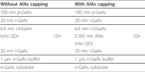
Table 1 Layer structures for samples without and with AlAs capping
Without AlAs capping With AlAs capping
100 nm p-GaAs 100 nm p-GaAs
20 nm i-GaAs 20 nm i-GaAs
6.6 nm i-InGaAs 6.6 nm i-InGaAs
InAs QDs 10× 0.283 nm AlAs 10×
InAs QDs
20 nm i-GaAs 20 nm i-GaAs
1μm n-GaAs buffer 1μm n-GaAs buffer
The curves of current density versus voltage (J-V) of samples A and B are shown in Figure 2b, while those for samples C and D are shown in Figure 3b. The fill factors, illumination short-circuit current densities (Jsc),
open-circuit voltages (Voc), and maximum power density
(VMJM) are summarized in Table 3. The fill factor is
cal-culated according to the equation:
FF=(V JM M) / (VOC SCJ ).
Jscfor all the samples are similar except for sample C.
As seen from the AFM images in Figure 1, sample C has deep holes on the surface. Their effect on the device performance is thus far unclear and is currently under investigation. From Table 3, one can see that the open-circuit voltages of the samples (samples A and B) with as-grown InAs QDs have higher values. Also, for the samples with one monolayer AlAs layers (samples B and D), the open-circuit voltages are improved compared to samples without one monolayer AlAs capping layers (samples A and C). Looking at the fill factors and open-circuit voltages, one can conclude that both quantities are higher for samples with AlAs layers than those of samples without AlAs layers, no matter with as-grown QDs or with annealed QDs. The reason for improve-ment of open-circuit voltages and fill factors in samples with a thin AlAs layer is currently under investigation.
Furthermore, by calculation of the power conversion efficiency (h) with the equation:
=V JM M / (P Pis the illumination power density),
we can conclude that with thin AlAs layers, the effi-ciency is enhanced by 6.15 and 2.75% for the devices with as-grown QDs and annealed QDs, respectively.
[image:3.595.55.542.101.139.2]Comparing Figures 2 and 3, one can see that the solar response spectra of samples C and D with annealed QDs are blue-shifted compared to those for samples A and B. The photo currents and open-circuit voltages of these samples with annealed QDs decrease. The blue-shift of the solar response spectra is probably due to the change of InAs composition, which decreases during annealing [7]. The decrease of photo currents can be related to the lower QD density due toin situannealing. A detailed explanation for this decrease in QD density
Table 2 Four types of samples
Sample A Sample B Sample C Sample D
With InAs QD layers As grown As grown Annealed for 5 min Annealed for 5 min
QDs are covered by 1 ML AlAs layers No Yes No Yes
[image:3.595.306.540.385.679.2]
Figure 1AFM images of device surfaces.(a)With as-grown InAs QDs and without AlAs layers (sample A),(b)with as-grown InAs QDs and AlAs layers (sample B),(c)with annealed InAs QDs and without AlAs layers (sample C), and(d)with annealed InAs QDs and AlAs layers (sample D).
[image:3.595.56.291.504.672.2]duringin situ annealing can be found in [7]. The holes and dashes are most likely the major reason for lower open-circuit voltage of the device with annealed QDs.
Conclusions
GaAs-basedp-i-n solar cells with a multistack of InAs QD embedded in InGaAs/GaAs matrix were fabricated by MBE. Post-growth annealing was used to tune the InAs QDs density. Annealing of InAs QDs introduces holes and dashes on the device surface and the solar
response spectrum is blue-shifted, while the fill factor decreases. With insertion of one monolayer AlAs cap-ping on top of the annealed InAs QDs for each layer in the stack, the dashes on the surface disappear and the density of holes decreases. The fill factors and power conversion efficiency and open-circuit voltages are improved, although the short-circuit current is reduced.
Abbreviations
AFM: atomic force microscopy; MBE: molecular beam epitaxy; QDs: quantum dots; RHEED: reflection high energy electron diffraction.
Acknowledgements
The authors acknowledge financial support from the Deutsche
Forschungsgemeinschaft (DFG) through grant DFG SCHA 1576/1-1, the U.S. National Science Foundation through Grant No. DMR 0806755, and the U.S. Department of Energy through Grant No. DE-FG36-08GO18016. Part of this study was also supported by DFG and the State of Baden-Württemberg through the DFG-Center for Functional Nanostructures (CFN) within subproject A2.6.
Author details
1Institut für Angewandte Physik/DFG-Center for Functional Nanostructures,
Karlsruhe Institute of Technology (KIT), Karlsruhe, Germany2Department of Electrical and Computer Engineering, Microelectronics Research Center, University of Texas at Austin, Austin, TX 78758, USA
Authors’contributions
DZH carried out growth of the devices and COMcP carried out electronic characterization of the devices. ETY and DMS conceived of the study, and participated in its design and coordination. All authors read and approved the final manuscript.
Competing interests
The authors declare that they have no competing interests.
Received: 26 September 2010 Accepted: 12 January 2011 Published: 12 January 2011
References
1. Green MA, Emery K, Hishikawa Y, Warta W:Solar Cell Efficiency Tables (Version 32).Prog Photovolt Res Appl2008,16:435.
2. King RR, Law DC, Edmondson KM, Fetzer CM, Kinsey GS, Yoon H, Sherif RA, Karam NH:40% efficient metamorphic GaInP/GaInAs/Ge multijunction solar cells.Appl Phys Lett2007,90:183516.
3. McPheeters CO, Hill CJ, Lim SH, Derkacs D, Ting DZ, Yu ET:Improved performance of In(Ga)As quantum dot solar cells via light scattering by nanoparticles.J Appl Phys2009,106:056101.
4. Ngo CY, Yoon SF, Fan WJ, Chua SJ:Effects of size and shape on electronic states of quantum dots.Phys Rev B2006,74:245331.
5. Ngo CY, Yoon SF, Fan WJ, Chua SJ:Tuning InAs quantum dots for high areal density and wideband emission.Appl Phys Lett2007,90:113103. 6. Ngo CY, Yoon SF, Tong CZ, Loke WK, Chua SJ:An investigation of growth
temperature on the surface morphology and optical properties of 1.3
μm InAs/InGaAs/GaAs quantum dot structures.Nanotechnology2007,
18:365708.
7. Hu DZ, Trampert A, Schaadt DM:Morphology and stress evolution of InAs QD grown and annealed in-situ at high temperature.J Cryst Growth2010,
312:447.
8. Moison JM, Guille C, Houzay F, Barthe F, Van Rompay M:Surface segregation of third-column atoms in group III-V arsenide compounds: Ternary alloys and heterostructures.Phys Rev B1989,40:6149. 9. Kawai T, Yonezu H, Ogasawara Y, Saito D, Pak K:Segregation and
interdiffusion of In atoms in GaAs/InAs/GaAs heterostructures.J Appl
Phys1993,74:1770.
10. Dorogan VG, Mazur YuI, Lee JH, Wang ZhM, Ware ME, Salamo GJ:Thermal peculiarity of AlAs-capped InAs quantum dots in a GaAs matrix.J Appl
[image:4.595.56.291.85.387.2]Phys2008,104:104303.
[image:4.595.56.297.641.732.2]Figure 3Photocurrent spectra and current density-voltage ( J-V) curves of the devices with annealed QDs with (sample C) and without AlAs capping layers (sample D).(a)Photo-current spectra and(b)J-Vcurves.
Table 3 Summary of short-circuit current density, open-circuit voltage, fill factor, and maximum power density for samples A grown QDs without AlAs layer), B (as-grown QDs with AlAs layer), C (annealed QDs without AlAs layer), and D (annealed QDs with AlAs layer)
Sample A
Sample B
Sample C
Sample D
Short-circuit current density (mA/cm2)
-5.65 -5.56 -7.00 -5.26
Open-circuit voltage (V) 0.617 0.642 0.475 0.540
Fill factor 0.671 0.696 0.524 0.631
Maximum power density (VMJM)
11. Yu ET, Derkacs D, Lim SH, Matheu P, Schadt DM:Plasmonic nanoparticle scattering for enhanced performance of photovoltaic and photodetector devices.Proc SPIE2008,7033:70331V.
12. Riotte M, Fohtung E, Grigoriev D, Minkevich AA, Slobodskyy T, Schmidbauer M, Metzger TH, Hu DZ, Schaadt DM, Baumbach T:Lateral ordering, strain, and morphology evolution of InGaAs/GaAs(001) quantum dots due to high temperature postgrowth annealing.Appl Phys
Lett2010,96:083102.
13. Lee JH, Wang ZhM, Kim ES, Kim NY, Park SH, Salamo GJ:Various Quantum-and Nano-Structures by III-V Droplet Epitaxy on GaAs Substrates.
Nanoscale Res Lett2010,5:308.
14. Yokota H, Iizuka K, Okamoto H, Suzuki T:AlAs coating for stacked structure of self-assembled Inas/GaAs quantum dots.J Cryst Growth2007,
301-302:825.
doi:10.1186/1556-276X-6-83
Cite this article as:Huet al.:Improvement of performance of InAs
quantum dot solar cell by inserting thin AlAs layers.Nanoscale Research
Letters20116:83.
Submit your manuscript to a
journal and benefi t from:
7 Convenient online submission
7 Rigorous peer review
7 Immediate publication on acceptance
7 Open access: articles freely available online
7 High visibility within the fi eld
7 Retaining the copyright to your article