Physics and Astronomy Dissertations Department of Physics and Astronomy
5-1-2019
Two dimensional nano-structures
Herath Mudiyanselage Herath Mudiyanselage
Follow this and additional works at:https://scholarworks.gsu.edu/phy_astr_diss
This Dissertation is brought to you for free and open access by the Department of Physics and Astronomy at ScholarWorks @ Georgia State University. It has been accepted for inclusion in Physics and Astronomy Dissertations by an authorized administrator of ScholarWorks @ Georgia State University. For more information, please [email protected].
Recommended Citation
by
H. M. THAKSHILA M. HERATH
Under the Direction of Vadym M. Apalkov, PhD
ABSTRACT
The properties of a step-like defect on the surface of ultrathin topological insulator nanofilm
have been studied. The reflectance of an electron from such a defect for different parameters
of the nanofilm and the different parameters of the defect has been calculated. An electron
incident on a steplike defect not only produces reflected and transmitted waves but also
generates the modes, which are localized at the steplike defect. Such modes result in an
enhancement of electron density at the defect by≈60%. The magnitude of the enhancement depends on the parameters of the nanofilm and the height of the step and is the largest in the
case of total electron reflection. Next, the quantum dots in 2D materials such as topological
insulator nanofilm, germanene and phosphorene were introduced. In topological insulator,
We introduce a quantum dot as a bump at a surface of nanofilm. Such quantum dot can
localize an electron if the size of the dot is large enough, ∼ 5 nm. The other type of quantum dot is created in germanene. The band gap of buckled graphene-like materials
such as germanene, depends on the external electric field. Then a specially design profile of
electric field can produce trapping potential for electrons. Another type of quantum dot can
dots have also been studied. The effects of the temperature and the substrate modify the
model parameters and should not change the results considerably.
by
H. M. THAKSHILA M. HERATH
A Dissertation Submitted in Partial Fulfillment of the Requirements for the Degree of
Doctor of Philosophy
in the College of Arts and Sciences
Georgia State University
by
H M THAKSHILA M HERATH
Committee Chair: Vadym Apalkov
Committee: Gennady Cymbalyuk Unil Perera
Douglas Gies
Alexander Kozhanov
Electronic Version Approved:
and
ACKNOWLEDGEMENTS
I would like to thank my adviser, Prof. Vadym Apalkov for his guidance and enormous
support throughout this period. I would not have even think of doing this without his help.
Also I am very thankful for Dr. Unil Perera for giving me valuable advice whenever sought.
He never asks to make appointments whenever I want to get some advice. Moreover I thank
and do appreciate all the members of the committee for their valuable time reading my
dissertation and giving me their insightful comments and suggestions.
Also, in the last three years I have been working on a project in computational
neuro-science. Dr. Gennady Cymbalyuk has been assisting and serving me as my co-adviser. Also,
Dr. Suranga Edirisinghe is a collaborator in that project and helping me in learning and
using high performance computing resources at Georgia State University and Open Science
Grid. I am very thankful for Dr. Gennady Cymbalyuk and Dr. Suranga Edirisighe for
their valuable time and support. We have still been working on that project and there is
no component from that project in this thesis. However, due to that project I have gained
many professional skills and personal skills, especially ’never give up’. We expect to have
some outcomes in the future.
I thank Carola Butler for her support coordinating and assigning the laboratory classes.
I also wish to thank all the faculty and staff of Physics and Astronomy Department at GSU
for their constant support through out these years.
Also, I am very grateful for my parents for trusting me and letting me do everything as
I wish. I would also like to thank all my teachers and friends who I met so far in my life. I
would not come this far without any of you.
Again, I am deeply grateful for my adviser for giving me a peaceful, valuable and
TABLE OF CONTENTS
ACKNOWLEDGEMENTS . . . v
LIST OF FIGURES . . . viii
LIST OF ABBREVIATIONS . . . xvii
CHAPTER 1 INTRODUCTION . . . 1
1.1 Overview . . . 1
1.2 Quantum dots . . . 2
1.3 Evolution of topological insulators . . . 4
1.4 Graphene like materials : Silicene/Germanene . . . 14
1.5 Black Phosphorous . . . 19
CHAPTER 2 ELECTRON SCATTERING BY STEP-LIKE DEFECT IN TOPOLOGICAL INSULATOR NANOFILM . . . 25
2.1 Model and Main Equations . . . 25
2.2 Results and Discussion . . . 29
2.2.1 Reflectance . . . 29
2.2.2 Evanescent modes . . . 34
2.3 Conclusion . . . 40
CHAPTER 3 QUANTUM DOT IN TOPOLOGICAL INSULATOR NANOFILM 42 3.1 Model and Main equations . . . 42
3.2 Results and Discussion . . . 47
3.2.1 Energy spectrum . . . 47
3.2.2 Optical transitions . . . 50
3.3 Conclusion . . . 54
CHAPTER 4 QUANTUM DOTS IN BUCKLED GRAPHENE-LIKE MA-TERIALS . . . 58
4.1 Model and Main equations . . . 58
4.2 Results and Discussion . . . 64
4.2.1 Energy spectrum . . . 64
4.2.2 Optical transitions . . . 65
4.3 Concluding remarks . . . 71
CHAPTER 5 ELECTRON CONFINEMENT IN BLACK PHOSPHO-RUS . . . 72
5.1 Energy spectrum . . . 72
5.2 Intranband and Interband optical transitions . . . 79
CHAPTER 6 CONCLUSIONS . . . 88
6.1 Conclusions . . . 88
LIST OF FIGURES
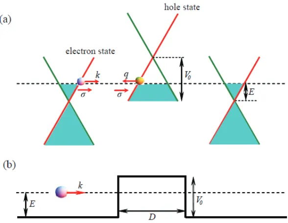
Figure 1.1 Tunnelling through potential barrier in graphene. The dashed line
represents the Fermi energy level, E. HereV0(> E) is the height of the potential barrier. σis the pseudospin. (a) The gapless linear dispersion of graphene is shown here. The blue filled areas indicate the occupied
states. k and q are wave vectors of the electron outside and inside of
the potential barrier respectively. (b) D is the width of the potential
barrier. Outside the potential barrier, the electron is in the conduction
band and inside it is in the valence band. The gapless states allows
the electrons to be in any quantum state regardless of the energy of
the electron. Due to that, electron penetrates through the potential
barrier which is known as Klein tunneling. Figure is taken from Ref.
[35] . . . 4
Figure 1.2 (color)Schematic illustration of quantum dot in topological insulator
nanofilm. The red and blue color bands are conduction and valence
band states respectively. TI nanofilm has gapped energy dispersion. V0 is the potential barrier. Outside the potential barrier, the electron’s
energy is in the conduction band. Inside the potential barrier, the
electron has no energy states to transit from valance to conduction
due to the gapped dispersion. The electron is trapped inside the TI
nanofilm with potential barrier. . . 5
Figure 1.3 (a) Electron backs off from the edge and keeps moving in the same
direction. The edge is in between the vacuum and the bulk which are
insulators. (b) conduction band and valence band touch as edge state
Figure 1.4 (a) Quantum Hall system : applied magnetic field makes electrons to
flow around the edge of the material (b) Quantum Spin Hall system
: The direction of the flow depends on the spin direction. Spin-orbit
interaction induces spin dependent magnetic field here. Figure is taken
from Ref. [41]. . . 8
Figure 1.5 (a) Electrons are localized in the bulk of the material and there are
gapped surface states. (b) Due to a magnetic field, electrons in the
bulk move in quantized orbits. The electrons near the edge bounce off
from the boundary as they are not able to complete circles. However
they keep moving forward and result in edge states. (c) Due to spin
degeneracy, electrons with spin up move in one direction and spin down
electrons move in the opposite direction. Two edge states are gapless
while the bulk has a finite gap. Figure is taken from Ref. [42]. . 9
Figure 1.6 (a) HgTe quantum well structure. Here d is the thickness of the HgTe
layer. (b) 2D band inversion is shown here as d increases. Figure is
taken from Ref. [38]. . . 9
Figure 1.7 (a) Crystal structure of Bi2Se3 topological insulator. The inset shows the enlarged version of an quintuple layer. (b) Band inversion of Bi
and Se atoms. Figure is copied from [59]. . . 15
Figure 1.8 Band structure formation of Bi2Se3. (I) Coupling of Bi and Se layers. (II) Creation of bonding and anti-bonding states (III) Energy
split-ting between p orbitals. (IV) Crossing of the levels due to spin orbit
interaction. Figure is copied from Ref. [58]. . . 16
Figure 1.9 Crystal structure of low-buckled Silicene and Germanene. (a),(b) The
side view and top view of Silicene. Atoms of two sublattices are
de-noted by red and yellow color.(c),(d) The side and top view of Ge.
Yellow and blue color atoms are used to represent atoms in two
Figure 1.10 (a),(b) Top and side view of Silicene structure. A and B atoms are on
two sublattices which separate by a perpendicular distance 2l. Electric
field Ez is applied perpendicular to the sheet (c) The band gap ∆ as
a function of Ez. As Ez increases topological phase transition occurs
between topological insulating phase to band insulating mode. Figure
is taken from [34] . . . 20
Figure 1.11 (Color) The 3D view of monolayer lattice structure of black
phospho-rous. A single layer consists of two sub lattices. Figure is copied from
[69]. . . 21
Figure 1.12 (a) Bulk BP consists with three stacked layers. (b) Side view shows
the armchair orientation. (c) Top view of BP in x-y plane shows
ori-entations of armchair and zigzag. Figure is copied from [70]. . . . 22
Figure 1.13 (Color) Energy dispersion of CB for phosphorene QD Eq. 1.22. . 23
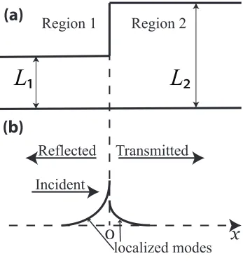
Figure 2.1 (a) Schematic illustration of a step-like defect on a surface of
topo-logical insulator nanofilm. The step-like defect at x = 0 divides TI nanofilm into two regions: region 1 with nanofilm thickness L1 and region 2 with nanofilm thickness L2. (b) Schematic illustration of electron reflection from the step-like defect. Incident, reflected, and
transmitted propagating waves are shown by arrows. The localized
modes, generated by electron reflection, are also shown. The modes
are localized at the defect. . . 30
Figure 2.2 Electron reflectance is shown as a function of the thickness L2 (see Fig. 2.1) of nanofilm in region 2 for different values of electron energy.
Figure 2.3 Electron reflectance is shown as a function of the wave vector,k, of the incident electron for different thicknesses L2 of TI nanofilm in region 2. The thickness of TI nanofilm in region 1 isL1 = 40 ˚A and the angle of incidence is ϕ= 0. The numbers next to the lines are the values of the thickness L2. . . 32 Figure 2.4 Electron reflectance is shown as a function of angle of incidence, ϕ,
for different values of the nanofilm thickness, L2, in region 2. The thickness of the nanofilm in region 1 isL1 = 40 ˚A and the wave vector of the incident electron is (a)k = 0.02 ˚A−1 and (b) k = 0.1 ˚A−1. The numbers next to the lines are the values of the thickness L2. In panel (a), the electron reflectance is exactly one atL2 = 10 ˚A and 20 ˚A. 35 Figure 2.5 Spatial distribution of electron density in the evanescent (localized)
modes is shown for different parameters of the nanofilm and different
electron energies (wave vectors). Two densities ρ1 and ρ2 correspond to two components of the wave function. The parameters of the
sys-tem (thicknesses L1 and L2 and electron wave vector k) are shown in corresponding panels. . . 36
Figure 2.6 The electron density in the evanescent mode near the step-like defect
in region 1, i.e. at x = 0−, is shown as a function of the nanofilm thickness L2 in region 2. Two densities ρ1 and ρ2 correspond to two components of the wave function. The nanofilm thickness in region 1 is
L1 = 40 ˚A and the wave vector of the incident electron is (a)k= 0.05 ˚
A−1 and (b) k = 0.1 ˚A−1. Singularities in the graphs at L
Figure 2.7 The electron density in the evanescent mode near the step-like defect
in region 1, i.e. at x = 0−, is shown as a function of the angle of incidence. Two densities ρ1 and ρ2 correspond to two components of the wave function. The nanofilm thicknesses in region 1 isL1 = 100 ˚A and in region 2 is L2 = 10 ˚A. The wave vector of the incident electron is k= 0.05 ˚A−1. . . . . 39 Figure 3.1 (a)Schematic illustration of TI quantum dot of cylindrical symmetry.
The TI nanofilm has a thicknessL2. The quantum dot is introduced as region of nanofilm with thickness L1 and is characterized by its height
h=L1−L2 and radius R. (b) Band edge profile of TI quantum dot is shown schematically for conduction and valence bands of the system.
The bandgaps ∆g,1 and ∆g,2 are the bandgaps of TI nanofilm with thickness L1 and L2, respectively. . . 43 Figure 3.2 Energy levels of conduction band (positive energies) and valence band
(negative energies) are shown as a function of quantum dot radius R. Only the levels with angular momentum m= 0, 1, and 2 are shown. 48 Figure 3.3 Energy spectra of TI quantum dot are shown as a function of angular
momentum m for different radii R of quantum dot: (a) 50 ˚A, (b) 100 ˚
A, (c) 150 ˚A, and (d) 200 ˚A. AtR = 50 ˚A there is only one energy level in the conduction band. The dotted lines with arrows show the main
intraband (labels by letters ”A”) and interband (labeled by letters
”B”) optical transitions. . . 49
Figure 3.4 Absorption interband optical spectra are shown for different radii R
of quantum dot: (a) 100 ˚A, (b) 150 ˚A, and (c) 200 ˚A. The labels of
optical lines correspond to the labels of transitions in Fig. 3.3. The
Figure 3.5 Absorption intraband optical spectra are shown for different radii R
of quantum dot: (a) 100 ˚A, (b) 150 ˚A, and (c) 200 ˚A. The labels of
optical lines correspond to the labels of transitions in Fig. 3.3. The
optical spectra have one strong line with small satellites. . . 52
Figure 3.6 The electron charge density distribution is shown for quantum dot of
radius 150 ˚A. The density is shown for conduction band states with
angular momentum (a) m= 0 and (b) m= 1. The numbers ”1” and ”2” next to the lines correspond to the lowest energy state and the
first excited state with a given angular momentum, respectively. 55
Figure 3.7 The electron density distribution is shown for quantum dot of radius
150 ˚A for two states with angular momentum m = 0. The numbers ”1” and ”2” next to the lines correspond to the lowest energy state and
the first excited state, respectively. (a) The density of electron with
spin-up, |ψ1(ρ)|2; (b) the density of electron with spin-down, |ψ2(ρ)|2; c) the electron spin density, Ξspin(ρ). . . 56 Figure 4.1 (a) Schematic illustration of silicene/germanene quantum dot. Two
sublattices A and B of silicene/germanene are shifted in z-direction
by distance l. The quantum dot has a shape of a circle with radius
R. The quantum dot is created by applying nonhomogeneous electric field, which has different strength inside (ρ < R) and outside (ρ > R) quantum dot. Arrows show the direction and magnitude of applied
electric field. (b) Magnitude of applied electric field as a function of
polar coordinateρ. (c) Band diagram of silicene/germanen monolayer. The band gap, ∆, depends on z component of electric field, Ez. Such
Figure 4.2 Energy spectra of the conduction (positive energies) band and the
va-lence band (negative energies) of germanene quantum dot. The states
are characterized by angular momentum m. The energy spectra are shown for different values of electric field in the region of quantum
dot, Ezi, and different sizes of the quantum dot, R: (a) R = 700 ˚A,
Ezi = 90 meV˚A−1; (b) R = 1100 ˚A, Ezi = 90 meV˚A−1; (c) R = 700
˚
A, Ezi = 120 meV˚A−1; (d) R = 1100 ˚A, Ezi = 120 meV˚A−1. The
electric field outside quantum dot is Ezo = 10 meV˚A−1. The arrows,
labeled as Ai, show allowed intraband optical transitions between the
states of the conduction band. The arrows, labeled as Bi, show
al-lowed interband optical transitions between the states of the valence
and conduction bands. . . 63
Figure 4.3 Energies ofm= 1 levels as function of applied electric field Ezi in the
region of quantum dot. The size of the quantum dot is (a) R = 200 ˚
A, (b) R = 400 ˚A, (c) R = 700 ˚A, and (d) R = 1000 ˚A. The effective distance, lef f, characterizes the slope of the corresponding line. The
electric field in the region of the quantum dot is Ezi = 90 meV˚A−1.
The electric field outside quantum dot is Ezo= 10 meV˚A−1. . . . 66
Figure 4.4 Energies ofm= 2 levels as function of applied electric field Ezi in the
region of quantum dot. The size of the quantum dot is (a) R = 400 ˚
A, (b) R = 700 ˚A, and (c) R = 1000 ˚A. The effective distance, lef f,
characterizes the slope of the corresponding line. The electric field in
the region of the quantum dot is Ezi= 90 meV˚A−1. The electric field
Figure 4.5 Absorption interband optical spectra. The radius, R, of the quantum dot the electric field,Ezi, in the region of the quantum dot are: (a)R =
700 ˚A, Ezi = 90meV˚A−1 (b) R = 1100 ˚A, Ezi = 90 meV˚A−1 (c) R =
700 ˚A, Ezi = 120 meV˚A−1, and (d) R = 1100 ˚A, Ezi = 120 meV˚A−1.
The electric field outside quantum dot isEzo= 10meV˚A−1. The labels,
Bi, near the optical lines correspond to the labels of transitions shown
in Fig. 4.2. . . 68
Figure 4.6 Absorption intraband optical spectra for different number of electrons
in the quantum dot. The radius of the quantum dot is: (a),(b),(c)
R = 700 ˚Aand (d),(e),(f) R = 1100 ˚A. The electric field inside and outside quantum dot is Ezi = 120 meV˚A−1 and Ezo = 10 meV˚A−1,
respectively. Ne is the number of electrons in the quantum dot. The
labels, Ai, near the optical lines correspond to the labels of transitions
shown in Fig. 4.2. . . 70
Figure 5.1 Monolayer black phosphorous quantum dot with radius R and
thick-ness of one atomic layer. . . 73
Figure 5.2 Energy spectrum of Hamiltonian H0 as a function of angular momen-tum. The positive energies correspond to the CB and the negative
energies correspond to the VB. . . 78
Figure 5.3 Complete energy spectrum of (a) the conduction band and (b) the
valance band. Each plot contains energy levels corresponding to
Hamiltonian H0 and total Hamiltonian H. . . 79 Figure 5.4 Intraband optical transitions for y-polarized light of monolayer black
phosphorous quantum dot with radius R=5 nm and 10 nm. The
in-traband transitions are shown for (a) 1 electron, (b) 2 electrons, (c) 3
electrons, (d) 4 electrons and (5) 5 electrons in the QD. HereNe is the
Figure 5.5 Intraband optical transitions for x-polarized light of monolayer black
phosphorous quantum dot with radius R=5 nm and 10 nm. The
in-traband transitions are shown for (a) 1 electron, (b) 2 electrons, (c) 3
electrons, (d) 4 electrons and (e) 5 electrons in the QD. HereNe is the
number of electrons. . . 84
Figure 5.6 Intraband optical transitions of QD for x-polarized light and
y-polarized light. The radius of QD is 5nm. The number of electron
in QD is (a) 1 electron, (b) 2 electrons, (c) 3 electrons, (d) 4 electrons
and (e) 5 electrons. . . 85
Figure 5.7 Interband optical transitions in phosphorous QD. The spectra are
shown for (a) x-polarized light and QD of radius 5 nm, (b) x-polarized
light and QD of radius 10 nm, (c) y-polarized light and QD of radius
5 nm, (d) y-polarized light and QD of radius 10 nm. . . 86
Figure 5.8 Interband optical transitions for x-polarized (black line) and
y-polarized (dashed color line) light in a phosphorene QD. The radius of
LIST OF ABBREVIATIONS
• QHS - Quantum Hall System
• QSH - Quantum Spin Hall
• QSHE - Quantum Spin Hall Effect
• TI - topological insulator
• 2DTI - two dimensional topological insulator
• QD - quantum dot
• CB - conduction band
• VB - valence band
• SOC - spin orbit coupling
• IB - interband
• BP - Black Phosphorus
CHAPTER 1
INTRODUCTION
1.1 Overview
Discovery of new 2D materials has emerged thanks to graphene’s exciting electronic,
optical, thermal and mechanical properties. Subsequently, graphene-like materials such as
silicene, germanene and phosphorene were discovered. Moreover ultrathin topological
insu-lator nanofilm has been identified as another 2D material which has remarkable properties.
In this thesis, I study the energy spectra and optical properties of nano-structures in
ultrathin TI nanofilms, graphene like-materials, and phosphorene monolayer. First a
one-dimensional step-like defect on TI nanofilm is considered and the electron transport along
the surface of TI nanofilm is studied. Then the energy spectra and optical transitions
of a confined Dirac electron in TI nanofilm, graphene-like materials such as silicene and
germanene and phosphorene are studied. To confine an electron in Dirac materials, a band
gap needs to be opened. For TI nanofilms, such a gap can be opened through hybridization of
the states at two opposite surfaces of the nanofilm. The band gap of graphene-like materials,
such as silicene or germanene, can be tuned by applying an electric field perpendicular to
silicene or germanene sheet. Monolayer or few layers of black phosphorus (BP) has an
intrinsic band gap and it can be controlled with the thickness of the BP sheet. In the
next section I discuss the general properties of quantum dots. Then the properties of TIs
and TI nanofilms, silicene/germanene and black phosphorus are studied. In Chapter 2, the
electron propagation along the step-like defect on TI nanofilm is considered. The results
are published in Physical Review B [1]. In Chapters 3, 4, and 5 I discuss the electronic
and optical properties of a confined Dirac electron in TI nanofilm, silicene/germanene and
phosphorene quantum dots, respectively. The results in Chapters 3 and 4 are published in
1.2 Quantum dots
Quantum dots are nanocrystals and often referred to as artificial atoms because the
confining potential replaces the potential of a nucleus. Usually a quantum dot can trap 2-200
electrons and the dot size varies from 10nm to 100nm [4]. Unique properties of quantum dots
are determined by their discrete energy spectrum, which can be tuned externally through the
nature and the strength of the confinement potential [5]. Such zero dimensional systems show
both specific electron transport with nonlinear features and controllable optical properties.
The main interest in quantum dots is related to their potential for applications, ranging from
novel lasers, light-emitting diodes, diode lasers, and photodetectors to quantum information
processing.
In conventional semiconductor systems, quantum dots are introduced either by
plac-ing one nano-sized material into another material, e.g., by the Stranski-Krastanow growth
technique, or by applying specially designed electrostatic confinement potential to
low-dimensional systems. In both cases a confinement potential is introduced, which results
in electron localization within the quantum dot region. The key concept here is to
local-ize an electron through a confinement potential. Recently, a new type of quantum dots,
graphene quantum dots [6–8] with electrostatic confinement potential, were considered. The
electrons in graphene behave as massless Dirac fermions. In graphene quantum dots due to
Klein paradox (Fig. 1.1), the electrons cannot be localized but can be only trapped for a
long time [7]. The longest trapping time is realized in a confinement potential with smooth
boundaries [8]. Such non-conventional behaviour of electrons in graphene is determined by
their unique low-energy dispersion, which is gapless and relativistic, while the corresponding
states are chiral [9, 10].
Other systems which have a dispersion law similar to graphene and corresponding
will be presented in the next section.
Similar to graphene, the conventional quantum dots, which can localize an electron,
cannot be realized in TIs through electrostatic confinement potential. To introduce a
quan-tum dot in TI, one can consider a TI of a finite nano-scale size [18, 19] or introduce a gap
in the dispersion law of coupled surface states of TI nanofilm [1, 20, 21]..Due to the finite
extension of the surface states into the bulk, the surface states at two surfaces of TI nanofilm
are coupled. Such coupling introduces a gap in the energy dispersion law. The magnitude
of the gap depends on the film thickness. Thus the trapping potential in this case can be
realized through modulation of the film thickness [2], which results in modulation of the
band gap. The schematic illustration of quantum dot in TI nanofilm is shown in Fig. 1.2.
Since TI nanofilm itself has a bandgap, an electron, confined in TI nanofilm QD, has no
energy states in the continuum to escape from the quantum dot.
In Chapter 3, we consider a quantum dot in TI nanofilm. A quantum dot is introduced
as a finite region of TI nanofilm with a larger thickness. Due to a gapped structure of the
energy dispersion in TI nanofilm, such quantum dot can localize an electron. We consider
only a single electron problem and for a single electron, both the energy spectra and the
optical transitions within TI quantum dot were calculated.
Other Dirac 2D materials, in which the gap can be opened, are buckled graphene-like
materials, such as silicene and germanene [22–30]. The main difference between
silicene/ger-manene and graphene is that due to a larger radius of a Si/Ge atom compared to a C atom,
the corresponding hexagon lattice in silicene/germnene has buckled structure [27] consisting
of two sublattices that are displaced vertically by a finite distance Lz ∼0.5 ˚A. As a result,
silicene has large spin-orbit(SO) interaction, which opens up band gaps at the Dirac points
(the band gap is ≈ 1.55−7.9 meV for silicene [31, 32] and ≈ 24−93 meV for germanene [31, 32]). For graphene, the corresponding spin-orbit-induced gap is very small, 25µeV [33]. The buckled structure of silicene/germanene lattice allows the band gap to be tuned almost
linearly by an external electric field applied perpendicular to the film [34]. Therefore in the
Figure (1.1) Tunnelling through potential barrier in graphene. The dashed line represents the Fermi energy level, E. Here V0(> E) is the height of the potential barrier. σ is the pseudospin. (a) The gapless linear dispersion of graphene is shown here. The blue filled areas indicate the occupied states. k and q are wave vectors of the electron outside and inside of the potential barrier respectively. (b) D is the width of the potential barrier. Outside the potential barrier, the electron is in the conduction band and inside it is in the valence band. The gapless states allows the electrons to be in any quantum state regardless of the energy of the electron. Due to that, electron penetrates through the potential barrier which is known as Klein tunneling. Figure is taken from Ref. [35]
a spatially dependent bandgap, which can produce electron localization.
In chapter 4, we study silicene/germanene quantum dots, which have cylindrical
sym-metry and are characterized by radius R. Such quantum dots are produced by a special distribution of external perpendicular electric field, which has different values in two regions:
ρ < R and ρ > R where ρ is the radial distance. The results are published in Ref. [3]
1.3 Evolution of topological insulators
Conventionally solid state materials can be divided into conductors, insulators, and
[image:24.612.151.445.91.319.2]No states
No states
V
o
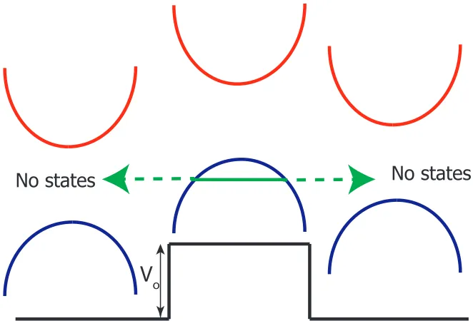
[image:25.612.140.471.232.457.2]Figure (1.3) (a) Electron backs off from the edge and keeps moving in the same direction. The edge is in between the vacuum and the bulk which are insulators. (b) conduction band and valence band touch as edge state becomes metallic. Figure is taken from Ref. [38]
new quantum states of matter is one of the most attractive topics in condensed matter
physics. Two-dimensional electron systems at low temperatures and high magnetic fields
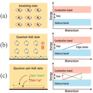
have metallic edge states and insulating bulk properties. This new quantum state was
discovered in 1980 and is called the quantum Hall (QH) state [36]. In this QH state, electrons
in the bulk follow quantized circular orbits due to the strong magnetic field. However,
electrons on the edge cannot complete a circular orbit. They hit the boundary, reflect, and
keep propagating along the edge. This is a drift motion, the direction of which depends
on the direction of the magnetic field. The quantum Hall system(QHS) has gapless edge
states and insulating bulk, see - Fig. 1.3. Only ”one-way” edge state exists due to external
magnetic field. The corresponding Hall conductivity is a multiple integer ofe2/hindependent of material [37].
In Mathematics there is a branch called topology. If two objects can be smoothly
trans-formed into each other through continuous deformation without changing their properties,
they are called topologically equivalent, i.e., they are in the same topological class. For
example, an orange and a ball are in one class as they both have zero number of holes or
genus(g) and one object can be transformed into another one without changing the number
deformed into a coffee cup while preserving its property a number of genus, a single hole.
In quantum mechanics, the main object of topology is a Hamiltonian. The two quantum
systems are called topologically equivalent if the Hamiltonian of the first system can be
continuously transformed into the Hamiltonian of the second system without closing the
bulk energy band gap. Similar to genus in Mathematics, topological classes in quantum
mechanics can be distinguished by a topological invariant called the Chern invariant n. If the Chern invariant remains constant when the Hamiltonian is deformed, it is called
topologically invariant. This is valid only for gapped materials such as insulators and gapped
superconductors. Topological classes are protected by the symmetry of a system.
A new quantum state, which belongs to a new topological class of materials called 2D
topological insulator (TI) or QSH state, has been theoretically predicted in 2006 [39] and
experimentally observed in HgTe/CdTe quantum wells in 2007, base temperatureT <30mK [40]. 2DTI or QSH state is invariant under TR symmetry and has strong intrinsic spin-orbit
coupling. Electrons with spin-up move in one direction and spin-down electrons move in the
opposite direction and no backscattering is allowed - see Fig. 1.4. The QH system requires
a magnetic field to create edge state while spin-orbit interaction plays the role of magnetic
field in QSH. The energy dispersions of different quantum states are shown in Fig. 1.5. In
QH system and QSH system, there is a ’one-way’ edge current while the bulk material has
a band gap. The difference in two systems is that QSH edge states are spin-split due to the
spin-orbit coupling. This splitting is called the Rashba splitting.
The trivial insulator and 2D TI cannot be transformed into each other without closing
a gap, i.e., they belong to two different topological classes. Let us consider the HgT e/CdT e
quantum well system. HgTe and CdTe are II-VI semiconductors which have strong spin-orbit
interactions. In CdTe s-states on the group II atom contribute to the conduction band and
p-states of VI atom contribute to the valence bands. In HgTe, p-states rise above s-states and
2D band inversion occurs. When HgTe is sandwiched in between CdTe layers, the 2D electron
structure can be tuned with the quantum well thickness d - see Fig. 1.6. If d < dc = 6.3nm
Figure (1.4) (a) Quantum Hall system : applied magnetic field makes electrons to flow around the edge of the material (b) Quantum Spin Hall system : The direction of the flow depends on the spin direction. Spin-orbit interaction induces spin dependent magnetic field here. Figure is taken from Ref. [41].
d > dc. The band structure gets inverted as the well thickness increases. At d = dc the
quantum well has a gapless band structure which indicates the phase transition from trivial
insulator to quantum spin Hall insulator or 2D topological insulator. The experiments have
shown that ifd > dc the quantum hall system has helical edge states [39, 43]. The significant
idea here is that a normal insulator becomes a topological insulator when the band structure
is inverted, so that they do not belong to the same topological class.
Soon after the discovery of 2D TI, three-dimensional TIs were predicted theoretically
and observed experimentally in BixSb1−x, Bi2Te3, Sb2Te3, and Bi2Se3 materials [11–17]. The unique feature of 3D TI is the gapless surface states with low-energy dispersion, which is
similar to the dispersion law of massless Dirac fermions. Such a relativistic dispersion law has
been observed experimentally by angle-resolved photoemission spectroscopy [13, 14, 16, 17,
44], oscillations in the local density of states [45], magnetoconductivity measurements[46],
quantum oscillations of magnetization [47], Aharonov-Bohm oscillations in TI nanoribbons
(a)
(b)
(c)
Figure (1.5) (a) Electrons are localized in the bulk of the material and there are gapped surface states. (b) Due to a magnetic field, electrons in the bulk move in quantized orbits. The electrons near the edge bounce off from the boundary as they are not able to complete circles. However they keep moving forward and result in edge states. (c) Due to spin degeneracy, electrons with spin up move in one direction and spin down electrons move in the opposite direction. Two edge states are gapless while the bulk has a finite gap. Figure is taken from Ref. [42].
[image:29.612.141.464.85.407.2][53].
Thus, topological insulators, 2D or 3D, should have strong spin-orbit interaction, which
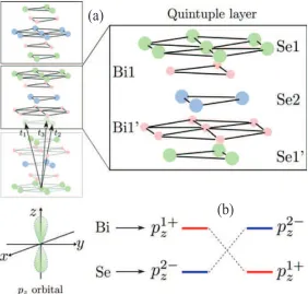
creates band inversion. The largest bulk gap of 3D TI is realized in Bi2Se3 TI with the bulk band gap of 0.3 eV. The crystal structure of well known real 3D topological insulator
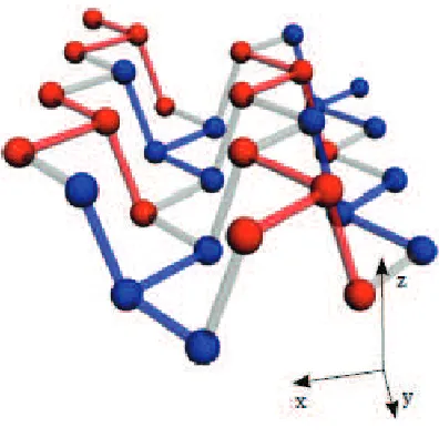
mate-rial, Bi2Se3, is shown in Fig. 1.7. The crystal structure has inversion symmetry I, three fold rotation symmetry C3 along the z-axis and time-reversal symmetry T. There are five atoms in a unit cell. Five-atom layers stack on top of each other, and this combined layer is called
a quintuple layer. A quintuple layer has two Bi layers, two Se layers and another Se layer
which acts as an inversion center. Though there is a weak interaction between two quintuple
layers, there is a strong SO coupling within a single quintuple layer. This strong SO coupling
can invert bands near the Γ point which makes this material a topological insulator.
The growing interest in 3D TI systems is related to the unique relativistic massless energy
dispersion law of their surface states. The surface states also have chiral spin texture, i.e.,
the direction of electron spin is correlated with direction of its momentum. The low energy
dispersion is of relativistic Dirac type. In general TIs can have an odd number of Dirac
cones, but in experimentally realized 3D TI systems, there is only one Dirac cone. Such a
Dirac cone is described by an effective Hamiltonian of relativistic type.
The relativistic massless dispersion law is also realized in another system - graphene [54].
Although the low energy dispersions in TI and graphene are similar, there is a fundamental
difference between these systems. Namely, TIs have only one Dirac cone (or odd number of
Dirac cones), while graphene has two Dirac cones, corresponding to two valleys. The states
of each Dirac cone in graphene are chiral, but chirality corresponds to pseudospin, not the
real spin, while the states of TI are spin chiral, where the real electron spin is correlated
with its momentum. Thus, each state in graphene has double spin degeneracy, whereas the
states in TI have no spin degeneracy.
Another fundamental difference between graphene and TI is that the surface states in
graphene are purely two-dimensional, whereas the surface states of TI are three-dimensional
of TI brings additional features to TI systems. For example, for TI nanofilm of small
thick-ness, the surface states at two boundaries of the nanofilm are coupled due to the 3D nature
of TI surface states [20, 55, 56]. Such coupling of the states of two TI surfaces opens a gap in
otherwise gapless surface relativistic dispersion, resulting in an energy dispersion similar to
the dispersion of narrow-gap semiconductors. The value of the gap depends on the thickness
of TI nanofilm. Studying surface states provides better understanding of TI nanofilm.
We consider Bi2Se3TI thin film grown along z-direction. The atomic p orbitals of Bi(6s26p3) and Se(4s24p4) contribute to the Hamiltonian. Formation of the band structure of 3D TI is illustrated in Fig. 1.8 and can be explained as follows. (1) Coupling of Bi and Se layers
makes Bi energy levels higher than Se energy levels due to the level repulsion. The p orbitals
of Bi and Se are hybridized and result in new states Bx,y,z, B
′
x,y,z, Sx,y,z, S
′
x,y,z and SOx,y,z− .
(2) The bonding and anti-bonding states,P1±
x,y,z andP2±x,y,z are created due to the inversion
symmetry. (3) The crystal has a layered structure which results in energy splitting between
pz and px,y. (4) The coupling between spin and orbital angular momentum leads to
cross-ing of the levels P1+
z and P2−z. It transforms the system into a topological insulator phase
[57, 58]. So P1+
z,↑(↓) and P2−z,↑(↓) are the closest energy levels to the Fermi level and
are considered as the basis of the effective Hamiltonian. The corresponding basis states can
be written as [ϕ(A1),0]T, [0, χ(−A1)]T, [χ(A1),0]T and [0, ϕ(−A1)]T. With this basis states, we can write down the effective Hamiltonian for bulk Bi2Se3 following Ref.
citeshan2010effective:
H(k) = ǫ0(k)I4×4+
M(k) A1kz 0 A2k−
A1kz −M(k) A2k− 0 0 A2k+ M(k) −A1kz
A2k+ 0 −A1kz −M(k),
, (1.1)
where I4×4 is 4×4 unit matrix, ǫ0(k) = C +D1kz2 +D2k2, M(k) = M − B1kz2 −B2k2,
k± = kx ±iky and k2 = kx2 + k2y. Here k is the finite wave vector. Model parameters
B2 = 56.6eV˚A2, C=−0.0068eV, D1 = 1.3eV mathrm˚A,D2 = 19.6eV mathram˚A. We solve the eigenvalue problem following Ref. [21]
H(k, kz)ψ =Eψ, (1.2)
using the four component trial wave function ψ = ψλeλz. The secular equation gives four
solutions ofλ(E) ,±λ1 and±λ2. We label them asβλα(E) withα∈
1,2 andβ ∈+,− .
λα(E) =
−2DF
+D−
+ (−1)α−1 √
R
2D+D− 1/2
, (1.3)
where
F =A21+D+(E−L1) +D−(E−L2),
R =F2−4D+D−[(E−L1)(E−L2)−A22k+k−],
D± =D1±B1,
L1 =C+M + (D2−B2)k2,
L2 =C−M + (D2+B2)k2.
Due to the double degeneracy each wave function can be written as
ψαβ1 =
D+λ2α+L2+E
−iA1(βλα)
0
A2k+
, (1.4)
ψαβ2 =
A2k− 0
iA1(βλα)
D−λ2
The general wave function is a linear combination of these eight functions
Ψ(E, k, z) = X
α=1,2 X
β=±γ
X
γ=1,2
Cαβγψαβγeβλαz, (1.6)
where Cαβγ is the superposition coefficient. Using the semi infinite boundary conditions
Ψ(z = 0) = 0 and Ψ(z → +∞) = 0, the energy dispersion of the surface states can be written as
E± =C+
D1M
B1 ±
A2 r
1−(D1
B1
)2k+ (D 2−
B2D1
B1
)k2. (1.7)
The Fermi velocity near the Γ point is,
vF =
1
~
dE
dk (1.8)
= (A2/~) p
1−(D1/B1)2. (1.9)
For real roots λ1,2, the edge states decay near the surface (z = 0) and the decay length is of the order of the characteristic length 1/λ1,2. For a film of finite thickness, if the thickness is
∼1/λ1,2, then two states at opposite surfaces are coupled and a finite energy gap is opened. If λ1,2 is real, the gap ∆ =E+−E− at the Dirac point can be approximated by
∆≃ p 4|A1D+D−M|
B3
1(A21B1+ 4D+D−M)
e−λ1L, (1.10)
with the finite-thickness boundary conditions Ψ(z = ±L/2) = 0 where two boundaries are located at z = L/2 and z = −L/2. If λ1,2 are complex conjugates, then the gap can be written as [21]
∆≃ p 8|A1D+D−M|
−B3
1(A21B1+ 4D+D−M)
e−aLsinbL, (1.11)
where λ±=a±ib and
a≃ A1
2√−D+D−
, (1.12) b≃ s M B1 + A 2 1 4D+D−
The energy band gap decays exponentially as a function of the thickness of TI film. If the
thickness of the nanofilm is small, i.e., L≪1/λ, then
tanh(λ1L
2 ) = 0 =⇒λ1 =i
π
L, (1.14)
and
H=D1
π2
L2 +D2 ˆ
p2
~2 +
A2
~ (ˆσxpˆy−σˆypˆx) + (B1
π2
L2 +B2 ˆ
p2
~2)ˆτz⊗σˆz. (1.15) where ˆσi (i = x, y, z) are Pauli matrices corresponding to spin degrees of freedom, and
ˆ
τz(= ±1) is the Pauli matrix corresponding to electron pseudospin. We use this effective
continuous Hamiltonian in Chapter 2.
In Chapter 2, we introduce the step-like defect by changing the thickness of the nanofilm.
The thickness of the film changes the energy band gap. We study how electron reflectance
and transmittance depend on the parameters of the step-like defect and properties of TI
nanofilm. The results are published in Ref. [1]
1.4 Graphene like materials : Silicene/Germanene
Graphene is a monolayer of Carbon(C) atoms. The unique properties of graphene lead
scientists to study other elements in the same group of periodic table. As a result, other
monolayer materials such as Silicene and Germanene have been discovered [22–27]. Silicene
and Germanene are single layers of Si and Ge atoms, respectively. The main difference
between silicene/germanene and graphene is that due to a larger radius of a Si/Ge atom
compared to a C atom, the corresponding hexagonal lattice in silicene/germanene has a
buckled structure [27], consisting of two sublattices that are displaced vertically by a finite
distance l ∼ 0.5 ˚A Fig. 1.10. As a result, silicene has a large spin-orbit interaction, which opens up a band gap at the Dirac points (∆so ≈1.55−7.9 meV for silicene and ∆so ≈24−93 meV for germanene [31, 32]). For graphene, the corresponding spin-orbit-induced gap is very
(a)
(b)
[image:35.612.163.445.235.504.2]to incorporate silicene/germanene into current devices and to create new spintronic devices.
The growth temperature for silicene on a Ag(1 1 1) surface ranges from 220 to 260◦C [60]. Germanene can be grown on Au(1 1 1) at∼200◦C [29].
The lattice geometry of low-buckled monolayers of Silicene and Germanene is shown in
Fig. 1.9. The low-buckled structure with sp3-like hybridization is stable.
Silicene/Germanene are expected to be topological insulators as they have strong
in-trinsic spin-orbit coupling. Additionally these materials have properties similar to graphene
as they reside in the same group IV. First-principle calculations demonstrated QSHE in
Sil-icene/Germanene and showed a gap opening at the Dirac points due to spin-orbit coupling
[61].
The low energy effective Hamiltonian with SOC of planar silicene at the Dirac point K
has the following form
Hef f[K] ≈
−ξσz vF kx+iky
vF kx−iky
ξσz
, (1.16)
wherevF is the Fermi velocity near the Dirac point andσz is the Pauli matrix. The effective
SOC ξ for the planar silicene is [61]
ξ ≈2ξ02|∆ǫ|/ 9Vspσ2
,
where ∆ǫ is the energy difference between the 3s and 3p orbitals, ξ0 is half the intrinsic spin-orbit coupling, and Vspσ is the parameter that corresponds to theσ bond. The σ bond
is created by the 3sand 3porbits. The energy spectrum can be obtained from Eq. (1.16) as
E(−→k) =±p(vFk)2+ξ2. (1.17)
The energy gap is 2ξ at the Dirac points. Due to its fascinating buckled structure, the charge will be transferred from one sub-lattice to the other sub-lattice and will open the
gap can be controlled. When we apply electric field, Ez normal to silicene/germanene sheet,
the low-energy effective Hamiltonian is
Hη =~vF(kxτx−ηkyτy) +ητzh11+lEzτz, (1.18)
where
h11=−λSOσz −aλR(kyσx−ηkxσy). (1.19)
vF =
√ 3
2 at = 5.5×10⁵ms−1 is the Fermi velocity, a = 3.86 ˚Ais the lattice constant of the sublattice and τa is the Pauli matrix corresponding to pseudospin. The Hamiltonian (1.18)
will be discussed more in Chapter 4. The energy dispersion corresponding to the Hamiltonian
(1.18) is
εη =±
r
(~vFk)2+ (lE
z−s
q
λ2
SO+ (aλRk)2)2,
where s = ηsz and sz = ±1 is the electron spin and η = ±1 corresponds to the K or K’
Dirac points. The energy band gap at the Dirac points is
∆(Ez) = 2|lEz−ηszλSO|. (1.20)
According to Eq. (1.20) the gap closes at Ez = ηszEc where Ec = λSO/l. At the critical
electric fieldEc, the gap closes and silicene becomes semimetal. Elsewhere the gap is opened
and silicene is an insulator. If |Ez| < Ec it is a topological insulator, while if |Ez| >
Ec, silicene is a band insulator. Fig. 1.10 shows the change of the band gap as electric
field increases. Therefore in the case of silicene/germanene, application of a nonuniform
perpendicular electric field results in a spatially dependent bandgap. This property can be
used to design silicene-based quantum dots.
In Chapter 4, we study silicene/germanene quantum dots, which have cylindrical
sym-metry. Such quantum dots are created by the spatial distribution of an external
(a)
(b)
(c)
(d)
Figure (1.9) Crystal structure of low-buckled Silicene and Germanene. (a),(b) The side view and top view of Silicene. Atoms of two sublattices are denoted by red and yellow color.(c),(d) The side and top view of Ge. Yellow and blue color atoms are used to represent atoms in two sublattices. Figures are taken from Ref. [61, 62].
optical transitions of such silicene/germanene quantum dots. The results are published in
Ref. [3].
1.5 Black Phosphorous
A well known phosphorus allotrope is white phosphorus (WP),P4. The molecule has a tetrahedron structure with six single bonds and it has sp3 hybridization. Each atom has 3 bonds with its neighbors. White phosphorus is not a stable material. When WP undergoes
high pressure, it forms a tripod shape by breaking three bonds in P4. Instead of becoming a fully flat layer, it has a puckered surface due to sp3 hybridization. It is the most stable phosphorus allotrope which is called black phosphorus (BP). The structure of monolayer
black phosphorus is shown in Fig. 1.11. Due to the puckered honeycomb structure, each
phosphorene layer consists of two atomic layers which are separated by 2.244˚Avertically. In BP the puckered layers are stacked on top of each other and stay together by weak van
(a)
(b)
(c)
Figure (1.10) (a),(b) Top and side view of Silicene structure. A and B atoms are on two sublattices which separate by a perpendicular distance 2l. Electric field Ez is applied
per-pendicular to the sheet (c) The band gap ∆ as a function ofEz. As Ez increases topological
[image:40.612.140.461.162.542.2]Figure (1.11) (Color) The 3D view of monolayer lattice structure of black phosphorous. A single layer consists of two sub lattices. Figure is copied from [69].
”zigzag” on two sides of the structure - see Fig. 1.12. Due to the different orientations, BP
has highly anisotropic properties. BP has different Young’s modulus and ultimate strain
values for the armchair direction and zig-zag directions [63]. According to first principle
cal-culations, Young’s modulus along the armchair direction is 21.9N.m−1 while it is 56.3N.m−1 for the zig-zag direction. By solving the phonon Boltzman transport equation (BTE), the
thermal conductivity at 300 K is 30.15Wm−1K−1 in the zigzag direction and 13.65Wm−1K−1 in the armchair direction [64]. Similar to graphene, the mechanical exfoliation method can
be used to prepare a single to few BP layers [65–68]. Phosphorene is a 2D semiconcuctor
with a finite band gap, while graphene is a semi-metal with zero band gap.
A monolayer BP has a gap of 1.5−2 eV around the Γ point which is greater than the gap of 0.3 eV of bulk BP. This gap depends on the thickness of the BP layer [71]. In addition to the relatively large band gap, BP has other unique properties, such as carrier mobility up to
1000cm2V−1s−1. These properties can be tuned by the thickness of phosphorene. Moreover few-layer phosphorene can be used for field effect transistors at room temperature [67].
[image:41.612.203.401.81.278.2](c)
Figure (1.12) (a) Bulk BP consists with three stacked layers. (b) Side view shows the armchair orientation. (c) Top view of BP in x-y plane shows orientations of armchair and zigzag. Figure is copied from [70].
[69] and is in the following form [72]
H =
Ec+ηck 2
x+νcky2 γkx+βk2y
γkx+βk2y Ev−ηvkx2−νvk2y
. (1.21)
whereEc and Ev are the lowest energy of conduction band and the highest energy of valence
band. Then the band gap is ∆ = Ec −Ev ≈ 2 eV. The band parameters ηc,v and νc,v
are related to the in-plane effective masses and γ and β represent the coupling between the conduction and valence bands. The parameters have the following values [72]: ηc,v = ~2/0.4m0 = 19.0763 eV ˚A2,νc = ~2/1.4m0 = 5.4504eV ˚A2,νv = ~2/2.0m0 = 3.8153 eV
˚
A2,γ = 4a/π= 2.8393 eV ˚A,β = 2a2/π2 = 1.0077eV˚A2 and a= 2.23 ˚A. Here m
0 is the free electron mass. From the Hamiltonian (1.21) we can find the corresponding energy dispersion
[image:42.612.88.526.85.292.2]-0.1
-0.05
0
0.05
0.1
k
x
(
˚
A
−
1
)
-0.1
-0.05
0
0.05
0.1
k
y
(
˚
A
−
1
)
2.05
2.1
2.15
2.2
2.25
Figure (1.13) (Color) Energy dispersion of CB for phosphorene QD Eq. 1.22.
E+= 1 2(p+
p
p2 −4q), (1.22)
E− = 1 2(p−
p
p2−4q), (1.23)
where
p = Ec +Ev + (νc−νv)k2y,
q = (Ec+ηckx2+νck2y)(Ev−ηvk2x−νvky2)−(γkx+βk2y)2.
The energy of the conduction band is shown in Fig. 1.13. We can see that the energy
dispersion is highly anisotropic. We can create a finite phosphorene quantum dot by using a
piece of phosphorene itself or by trapping potential. Here we consider a piece of phosphorene
[image:43.612.121.487.93.338.2]the energy levels and the corresponding wave functions of such a quantum dot. Then we
CHAPTER 2
ELECTRON SCATTERING BY STEP-LIKE DEFECT IN TOPOLOGICAL
INSULATOR NANOFILM
By changing the thickness of the TI nanofilm one can control the gap in the dispersion
law and introduce the defects into the system. The simplest defect is a step-like defect,
which divides two regions of TI nanofilm with different thicknesses. Such type of defect with
the height of a step∼30.5 ˚A was introduced on a surface of Bi2Te3 to study experimentally the oscillations of the local density of states due to the step defect. The step-like defect was
also considered theoretically in Refs. [73, 74] within a 2D model of surface states of TI. The
defect was introduced into the 2D effective Hamiltonian of the surface states as a δ-function potential.
Here we consider the properties of a one-dimensional step-like defect on a surface of TI
nanofilm. An electron, propagating along the surface of TI nanofilm, can be scattered by the
defect, which results in generation of reflected and transmitted electron waves. We study how
electron reflectance and transmittance depend on the parameters of the defect. Although
some properties of the electron reflection can be explained within a picture of reflection
from a step-like barrier, there are properties which are specific to TI system. Namely, the
scattering of an electron by a step-like defect generates not only reflected and transmitted
electron waves, but also localized (evanescent) modes. Such modes are localized at the defect,
which results in an increase of the electron density at the defect.
2.1 Model and Main Equations
We consider a TI nanofilm with a step-like singularity, which means that the TI nanofilm
consists of two regions with different thicknesses – see Fig. 2.1(a). We assume that the linear
and axis z perpendicular to the nanofilm – see Fig. 2.1(a). In two regions, determined by the defect, the thickness of the nanofilm is L1 at x < 0 (region 1) and L2 at x > 0 (region 2). Below we consider both L1 < L2 and L1 > L2 cases.
We study the reflection (scattering) of an electron by the step-like defect. The electron,
propagating in region 1 in the positive direction of axis x, is incident on the defect and is partially reflected (transmitted) by the defect. The specific feature of TI system is that the
scattering of the incident electron by the defect produces not only the propagating (reflected
and transmitted) electron waves but also the evanescent (localized) waves as schematically
illustrated in Fig. 2.1(b).
To study the scattering of an electron by the step-like defect, we employ the effective
low energy model of TI nanofilm, which is described by 4×4 matrix Hamiltonian of the following form [21]
H =
H+ 0
0 H−
= D1
π2
L2 +D2 ˆ
p2
~2 +
A2
~ (ˆσxpˆy−σˆypˆx) + (B1
π2
L2 +B2 ˆ
p2
~2)ˆτz⊗σˆz. (2.1)
where ˆσi (i=x, y, z) are Pauli matrices corresponding to spin degrees of freedom, and ˆτz is
the Pauli matrix corresponding to electron pseudospin, which determines the block diagonal
Hamiltonian matrix with H+ (for τz = 1) and H− (for τz = −1). Here ˆpi = −~∂/∂ri
(i = x, y) is the electron 2D momentum, L is the thickness of the nanofilm, and A2, B1,
B2, D1, D2 are parameters of 3D model of TI. Below we consider Ti2Se3 TI, for which these parameters takes the following values [57] A2 = 4.1 eV·˚A, B1 = 10 eV·˚A2 , B2 = 56.6 eV·˚A2, D
1 = 1.3 eV·˚A2, D2 = 19.6 eV·˚A2. The third term in Hamiltonian (2.1), which is determined by constant A2, describes the spin-orbit interaction in the effective Hamiltonian of TI.
Since the electron dynamics for two components of pseudospin are decoupled, we
For such a component of pseudospin, the scattering is described by a 2×2 Hamiltonian, where the two components of the wave function correspond to two spin components, σz =±1. The
scattering amplitudes for pseudospin component τz =−1 are the same as forτz = 1.
Within each region (1 or 2) the nanofilm thickness is constant. Then the electron wave
functions corresponding to Hamiltonian (2.1) have the plane wave form Ψ ∝ ei(kxx+kyy),
where (kx, ky) is an electron wave vector. The corresponding energy spectrum, which is
given by expression
E±(k, L) =
D1
π2
L2 +D2k 2 ± s B1 π2
L2 +B2k 2
2 +A2
2k2, (2.2)
has a gap ∆g(L) = 2B1π
2
L2, which is determined by the thickness of the nanofilm. Here k = pk2
x+ky2. For a given wave vector (kx, ky) there are two energy bands, E+(k) and
E−(k), which can be identified as ”conduction” and ”valence” bands of TI nanofilm. The two component wave function, corresponding to wave vector (kx, ky) and energy E±(kx, ky)
have the following form
ˆ
Ψkx,ky,L =
1
q
A2
2|k|2+ (F1+N1k2−E±)2
×
−A2(ikx+ky)
F1 +N1k2−E±(k, L)
ei(kxx+kyy). (2.3)
where we introduced the following notations F1 = D1+B1
π2/L2 and N
1 = D2+B2
.
For the reflection (elastic electron scattering) problem, we need to identify the reflected
and transmitted states for a given incident electron wave. Such states are determined by the
condition that the energy of the reflected (transmitted) electron is equal to the energy of the
incident electron.
E =E±(k). These solutions are given by the following expressions
k1,±(E, L) = ± s
β+pβ2+ 4αγ
2α , (2.4) k2,±(E, L) = ±
s
β−pβ2+ 4αγ
2α , (2.5)
whereα=B2
2−D22,β = B1B2−D1D2 2π2
L2 + 2ED2+A22,γ =E E−D1
2π2
L2
+ (D2
1−B12)π
4
L4.
If energy E is not in the energy gap of TI nanofilm, then wave vectors k1,± are real and correspond to two propagating waves, whereas the wave vectors k2,± are purely imaginary and describe decaying and growing modes. If energy E is in the gap, i.e., E−(k= 0) < E <
E+(k = 0), then all solutions, k1,± and k2,±, are imaginary, which means that there are no in-gap propagating modes and all the modes are either decaying or growing modes.
The existence of four different wave vectors with the same energy introduces an additional
features in electron scattering by a defect in TI nanofilm. For a step-like defect the problem
of scattering (reflection) is formulated as follows. An electron with wave vector (kx >0, ky)
and energy E±(k) is propagating in the positive direction of axis x and is incident on the step-like defect. The direction of electron propagation is characterized by the angle of
inci-dence, π/2≥ ϕ ≥ 0, defined as tanϕ = ky/kx. The scattering of an electron by the defect
results in generation of two reflected and two transmitted propagating or evanescent waves,
see Fig. 2.1(b). Such waves are determined by the condition that the energy of the reflected
or transmitted wave is equal to the energy of the incident electron and the y component of the wave vector, ky, of the incident electron is equal to the y component of the transmitted
and reflected waves. Here for the reflected (transmitted) waves we need to choose the waves,
which propagate or decay in the negative (positive) direction of axis x.
The corresponding wave functions are described by Eq. (2.3) and are characterized by the
following parameters:
(i) the incident wave is ˆΨkx,ky,L1, where k =k1,+(E, L1) and E is the energy of the incident
(ii) the reflected waves are ˆΨ−kx,ky,L1 (propagating wave) and ˆΨ−iλ,ky,L1 (evanescent wave),
where λ >0 and−λ2+k2
y = [k2,+(E, L1)]2. (iii) transmitted waves are ˆΨk′
x,ky,L2 (propagating or evanescent wave) and ˆΨiλ′,ky,L2
(evanes-cent wave), where (k′
x)2+k2y = [k1,+(E, L2)]2, λ′ >0, and−(λ′)2 +ky2 = [k2,+(E, L2)]2. Then the electron wave function is
ˆ Ψ0 =
ˆ
Ψkx,ky,L1 +r1Ψˆ−kx,ky,L1+r2Ψˆ−iλ,ky,L1, x <0, t1Ψˆk′
x,ky,L2 +t2Ψˆiλ′,ky,L2, x >0,
(2.6)
where r1,r2 are amplitudes of the reflected waves and t1, t2 are amplitudes of the transmit-ted waves. The amplitudes r1, r2, t1, and t2 are found from the boundary condition, i.e., continuity of the wave function, ˆΨ0, and its derivative, ∂xΨˆ0, at x= 0, which is equivalent to continuity of the current (electron flux). Then the reflection and transmission coefficients
are R=|r2
1| and T = 1−R, respectively. Since the evanescent modes do not contribute to electron current, there is no contribution of the evanescent modes into the reflectance and
transmittance.
2.2 Results and Discussion
2.2.1 Reflectance
Since the evanescent waves produce zero current, only the propagating waves contribute
to the electron reflectance. Thus, if the energy of the incident electron, which is in the region
1 of the nanofilm with thickness L1, is in the energy gap of the TI nanofilm in region 2 with thickness L2, then there are no propagating transmitted waves and the transmittance in this case is 0, i.e., the reflectance is exactly 1. Such total internal reflection can be realized only
if ∆g(L1) = 2B1π
2
L2
1 <∆g(L2) = 2B1
π2
L2
2, i.e. L1 > L2.
If the energy of the incident electron is not in the gap of TI nanofilm in region 2 then
there is a finite reflectance of the incident electron. In Fig. 2.2 the reflectance is shown
L
1
L
2
Reflected
Transmitted
Incident
(a)
(b)
localized modes
x
0
Region 1 Region 2
[image:50.612.148.495.139.514.2]0
20
4060
80
1000
0.2
0.4
0.6 0.8 1.0
k=0.005Å-1
L
1
=
40 Å
j=
0˚
0.02
0.01
0.04
0.1
Re
fl
ec
ta
nc
e
L
2(Å)
0
0.02
0.04
0.06
0.08
0.10
0
0.2
0.4
0.6
0.8
1.0
L
2 =
10 Å
L
1
=
40
Å
20
j
=
0
°
30
50 100
R
ef
le
ct
an
ce
k
(
Å
-1)
Figure (2.3) Electron reflectance is shown as a function of the wave vector,k, of the incident electron for different thicknesses L2 of TI nanofilm in region 2. The thickness of TI nanofilm in region 1 is L1 = 40 ˚A and the angle of incidence isϕ = 0. The numbers next to the lines are the values of the thickness L2.
electron, i.e., for different energies of the incident electron. The thickness of the nanofilm
in region 1 is fixed and is equal to L1 = 40 ˚A. The reflectance is zero at L2 = L1 = 40 ˚
A, which corresponds to homogeneous TI nanofilm with constant thickness. At L2 6= L1 the reflectance is not zero, but it shows different behaviours for L2 > L1 and L2 < L1. At
L2 > L1 the reflectance monotonically increases with L2, reaching some asymptotic values at largeL2, which are around 20% - 40 % depending on the electron energy.
At L2 < L1, within a narrow interval of thickness L2, the reflectance shows very strong dependence on L2. At each value of electron energy (or wave vector), there is a critical thickness L(2cr) so that at L2 ≤ L(2cr) an electron experiences total internal reflection with reflectance equal to one. This corresponds to the condition that the electron energy E is in the energy gap of TI nanofilm in region 2. The critical thickness is determined by an
equationE+(0, L(2cr)) = E, which givesL (cr)
2 =
p
π2(D
within a narrow interval of thicknesses L2.
The reflectance as a function of electron wave vector (energy) is shown in Fig. 2.3 for different
values of L2. At L2 > L1 = 40 ˚A, the reflectance is large within narrow interval of wave vectors near k = 0 and becomes one at k = 0. At L2 < L1, there a range of wave vectors, which satisfy the condition of total reflection, i.e. the energy E is in the gap of nanofilm of thickness L2. The total reflection occurs at small wave vectors (small energies), i.e., at
k < k(cr)(L
2). The critical wave vector is determined by the condition that the electron energy is exactly at the edge of the ”conduction” band dispersion for the nanofilm of region
2. Thus, the critical wave vector satisfies an equation E =E+(k(cr), L2). The dependence of the reflectance on the wave vector (energy) is strong near the critical value, k ≈ k(cr). Within a good accuracy, one can say that the reflectance is one within a finite range of wave
vectors, k < k(cr)(L
2), and zero at k > k(cr)(L2).
This property can be used to design an electron filter to select electrons within a given
range of energies. Namely, if an electron beam with a broad energy distribution is incident
on a step-like singularity with the known values of L1 and L2 < L1, then only the electrons with k < k(cr)(L
2) will be totally reflected.
In Fig. 2.4 we show the dependence of the reflectance on the angle of incidence, ϕ, for different wave vectors (energies) of the incident electron and different thicknesses, L2, of TI nanofilm in region 2. The total internal reflection, which can be realized only at L2 < L1, occurs at ϕ > ϕ(cr). The critical angle is determined by condition E = E
+(ksinϕ(cr), L2), i.e., kx in region 2 is zero at the critical angle and the y component of the wave vector is
ksinϕ(cr). Comparing small [Fig. 2.4(a)] and large electron energies [Fig. 2.4(b)], one can see that the critical angle ϕ(cr) increases with electron energy. The critical angle also increases with the thickness L2. If the thickness L2 of the nanofilm in region 2 satisfies an inequality
E+(0, L2)≤E, then even at zero angle of incidence the electron experiences total reflection. In this case for all angles there is total internal reflection of the incident electron [seeL2 = 10 and 20 ˚A in Fig. 2.4(a) and L2 = 10 ˚A in Fig. 2.4(b)]. Near the critical angle ϕ≈ ϕ(cr) (at