o
MicroVAX
II System
Digital Technical Journal
ofDigital Equipment Corporation
Cover Design
Hardware, software, and peripheral devices for the Micro VAX 11 system are featured in this issue. Two VLSI devices, the 78032 CPU chip and the 78132 FPU chip, form the core of this system. Our cover shows the input programmable logic array for the FPU chip.
The cover was designed by Deborah Falck of the Graphic Design Department.
Production Staff
Production Editor- M. Terri Autieri Designer - Charlotte Bell
Typesetting Programmer -James K. Scarsdale
Advisory Board
Samuel H. Fuller, Chairman Robert M. Glorioso John W . McCredie John F. Mucci
Mahendra R. Patel Grant F. Saviers William D. Strecker Maurice V. Wilkes
The Digital Technical journal is published by Digital Equipment Corporation, 77 Reed Road, Hudson, Massachusetts 01749.
Comments on the content of any paper are welcomed. Write to the editor at Mail Stop HL02-3/KI1 at the published-by address.
Comments can also be sent on the ENET to RDVAX::BEANE or on the ARPANET to BEANE%RDVAX.DEC@DECWRL.
Copyright © 1986 Digital Equipment Corporation. Copying without fee is permitted provided that such copies are made for use in educational institutions by faculty members and are not distributed for commer cial advantage. Abstracting with credit of Digital Equipment Corporation's authorship is permitted. Requests for other copies for a fee may be made to the Digital Press of Digital Equipment Corporation. All rights reserved.
The information in this journal is subject to change without notice and should not be construed as a com mitment by Digital Equipment Corporation. Digital Equipment Corporation assumes no responsibility for any errors that may appear in this document. ISBN 932376-89-4
Documentation Number EY-3474E-DP
The following are trademarks of Digital Equipment Corporation: CompacTape, DEC, the Digital logo, MicroVAX, MicroVAX I, MicroVAX II, MicroVMS, PDP-7, PDP-I I , Q-BUS, RSTS, TK50, ULTRIX, ULTRIX-32, UN113US, VAX, VAX-ll/730, VAX-ll/750, VAX-ll/780, VAX 8600, VAX 8200, VAXELN, VAXstation, VMS, VT.
Apple II is a trademark of Apple Computer, Inc. AT&T is a trademark of American Telephone & Tele graph Company.
IBM is a registered trademark of International Business Machines, Inc.
Mylar is a trademark of E. I. duPont deNemours & Company.
Tek is a registered trademark of Tektronix, Inc. UNIX and System V are trademarks of AT&T Bell Laboratories.
Xerox is a registered trademark of Xerox Corporation. 68000 is a trademark of Motorola, Inc.
Contents
8
Foreword
jeffrey C. Kalb
12
The MicroVAX 78032 Chip, A 32-Bit Microprocessor
Daniel W. Dobberpuhl. Robert M. Supnik, Richard T. Witek24
The MicroVAX 78132 Floating Point Chip
William R. Bidermann, Amnon Fisher, Burton M. Leary, Robert J Simcoe, William R. Wheeler3 7
Developing the Micro VAX II CPU Board
Barry A. Maskas48
The Evolution of the Custom CAD Suite Used on the
Micro VAX
IISystem
Anthony F. Hutchings
56
The Making of a Micro VAX Workstation
Rick Spitz, Peter George. Stephen Zalewski66
The RQDX3 Design Project
Nicholas A. Warchol, Stephen F. Shirron76
The Evolution of Instruction Emulation for the
MicroVAX Systems
Kathleen D. Morse, Lawrence). Kenah
86
The TK50 Cartridge Tape Drive
Steven E. Doone, Guemer E. Schneider99
Porting ULTRIX Software to the Micro VAX System
Raymond J. Lanza
Richard W. Beane F.ditor
This issue of the journal is the second pub lished by Digital's engineering organization. Our first issue ( August 198 5 ) fe atured papers about the technologies us ed i n designing the VAX 8600 processor. The jour nal presents papers written by the technical contributors who design Digital's products . The information is directed at engineering faculty members, Digital's own engi neers, and customers.
This issue features the M icroV AX ll system , which imp lements the VAX architecture o n a single CPU chip, the 780 3 2 . Another chip, the 7813 2 , executes fast floating point oper ations ; a si ngle board holds both those chips, plus one m egabyte of memory. New per i pherals have been designed, and the VMS a n d ULTRIX s o ftware a d a p ted to the MicroVAX II syste m . This col l ecti o n of papers, by authors from different engineer ing groups, presents a wide spectrum of the MicroVAX II hardware and software.
The first paper, by Dan Dobberpuhl , Bob Supnik, and Rich Witek, is a description of the 780 3 2 CPU chip, which imp le ments a subset of the full VAX i nstruction set. The decisions a bout w hi c h i n s truc t i o n s to microcode are discussed , along with hard ware simplifications needed to fit functions on one chi p . The chip's various operations are explained, with emphasis on paral le l execution .
The CPU chip can use a coprocessor, the 78 1 3 2 FPU chip , to perform fast floating p oint o p e ra t i o n s . T h e p a p e r by B i ll Bidermann, Amnon Fisher, Mike Leary, Bob Simcoe , and Bill Wheeler relates t he 7813 2's arch itecture and algori thms. The protocol between the two chips is discussed and a
description is given of the wiring and signal i n t e g r i ty i s sues a n d how t h e y were addressed.
Both chips are mounted on a single board containing one megabyte of me mory. Barry Maskas' paper exp lains how the CPU board had to be designed as a linked sequential machine with dual ports . The development process is interesting because the board and the chips were designed in para l lel.
The paper on CAD tools , by Tony Hutch i ngs, relates the large role they played in the chi p and board designs . The various levels of CAD support , from be havioral modeling, t hrough logic and circuit simulation, to wire list generation is described.
The software gra p hics t hat turn t he MicroVAX II system into a single-user work station are reported in the paper by Rick Spitz , Peter George, and Steve Zalewski . The control of windowing software and virtual displays is discussed, as are the implementa tion details.
The RQDX3 disk controller provides fast data transfers between a CPU and disk stor age devices. Nick Warc hol and Stephen Shir ron explain the top-down development pro cess that lead to unique solutions to difficult problems. Their descri ption of the fi nal architecture shows how the original goa ls were met in the eventual design.
With a subset architecture , those instruc t ions not in the set have to be executed another way. The paper by Kathy Morse and Larry Kenah describes the macrocode emula tion of the VMS changes required to do that. The testi ng techniques are i nteresting since they were done without M icroVAX hardware . The paper by Steve Boone and Guenter Schne ider describes the TKSO, a streaming cartridge tape drive providing fast data trans fer. The authors d iscuss the unique cartridge, tape transport , and controller designs, high Iighting the self-thread i ng technique and the serpentine readjwrite process .
The fi nal paper, by Ray Lanza , describes porting the ULTRIX- 3 2 software to the MicroVAX processor. Ray explains the cross development environment and the mapping techniques that allowed the heart of the ULTRIX software to fit on a small system .
Biographies
4
William R. Bidermann Bill Bidermann is the engineering manager of the Advanced Development Memory Group. He consu lted on the float ing point chips for both the VAX 8 2 0 0 and MicroVAX II processors . Before joining Digital in 198 4, he was a consultant for Tenex and Rampower. Previously, he worked as a project manager at Hewlett Packard LaboratOries in Palo Alto, Cal ifornia, and as a design engineer at Texas Instru ments Central Research Labs . Bill received his S.B. and S . M . degrees i n electrical engineering and computer science from M . I .T. i n
1978
Steven E. Boone Steve Boone graduated from Michigan State Univer sity (B.S. E . E . , 1974) and the University of Mich igan (M.S. E .C . E ., 197 5). He has also done advanced graduate work at Southern Methodist Un iver sity. Before joining Digital in 1984, Steve worked as a principal hard ware engineer for Sequoia Systems, and as a senior design engineer at
Prime and Raytheon. For two years, he was an engineering supervisor working on the TK 50 controller design . Steve is currently the technical �ngineering manager for TK Cartridge Tape Su bsystem Engineering.
Daniel W. Dobberpuhl Dan Dobberpu hl is a senior consulting engi neer and manager of the Processor Advanced Deve lopment Group. On the MicroVAX II project, he led the implementation of the 78032 CPU chip. Previously, he consulted on CMOS, ZMOS, and TIPI technology development, and worked on the Til and F l l projects . Dan joined Digital in 1976 from General Electric Company. He received a B .S . E . E . degree from the University o f I l linois in 1967. A member o f IEEE, he holds fou r patents and is the coauthor of The Design and A nalysis of
VLS! Circuits.
Amnon Fisher Ed ucated at Israel Institute of Techno logy (B.S. E . E . ,
1973) and City College o f New York (M.S.E . E . , 1975), Amnon Fisher worked as both a contribu tor and project leader on the 3 20 16 CPU at National Semiconductor. join ing Digital in 1983, he was a project leader of the Vl l jSCORPIO floating point chip (VAX 8 2 0 0 system) , and a contrib u tOr tO the MicroVAX I I 78132 chip. Amnon is currently an engineering manager in the SemiconductOr Engineering Grou p , working on t h e design and deve lopment of a fou r-chip s e t VAX implementation .
for 16 years, he designed operating systems and was one of the VME· system architects on the 2900 series . He later became corporate man· ager of CAD . Tony joined Digital in 1 982 as the project manager for the proprietary DECSIM software and then became manager of the VLSI CAD Group. Tony, a member of IEEE and the British Computer Society, is currently chairman of the CAD section of the ICCD.
Lawrence J. Kenah Larry Kenah , a consulting software engineer in the VMS Development Group, wrote the decimaljstring emu lator for the MicroVA.X project. Since joining engineering i n 1 980, Larry has worked on the VMS nucleus in the areas of memory management, pro· cess scheduling, and image activation. He came to Digital in 1 9 7 5 as an instructor and course deve loper in Educational Services. Larry received his B.S. degree ( 1 968) from Boston College and his M . S. ( 1 970) and Ph . D . ( 1 977) degrees in high-energy physics from Northwestern Uni· versity. He is coauthor of VAXjVMS Internals and Data Structures.
Raymond J. Lanza Ray Lanza is currently the project leader for the ULTRIX- 3 2 system. After joining Digital in 1 98 3 , he ported the ULTRIX system to t he MicroVA.X I processor. As project leader, he ported the system to the Micro VAX I I processor in 1 9 8 4 . Ray received h is B . S .E.E.jC.E. degree from the University of New Hampshire in 1 980, then became the lead engineer in a UNIX group a t AT&T. Later he was a senior software engineer a t Wa ng Laboratories, Inc . , researc hing wi ndowing systems and UNIX distribu ted systems.
Burton M. Leary In 1 980, M ike Leary joined Digital after receiving his B.S. degree i n electrical engineering from the University of Massa· chusetts . In semiconductor engineering, he worked on chip designs and helped to develop the floating point chip for the MicroVA.X II system . Mike did behavioral model ing, wrote microcode , and designed the main sequencer for that chip. He is now a senior engineer in the Advanced Development Memory Group, designing the internal cache for an advanced chip project .
Barry A. Maskas Barry Maskas is a principal engineer cu rrently speci fying and designing an integrated circuit, and fiber-optic boards for future systems . As a senior engineer on the MicroVA.X I I project , he was co-designer of the CPU board and the memory boards. Barry came to Digital in 1 9 79 after receiving his B. S.E.E. degree from Pennsylvania State University. He also holds a n associate's degree from the Commu· nity College of Allegheny Cou nty and did u ndergraduate work at LSU . Barry is a member of Eta Kappa Nu ; he has a patent pending for a seJf. configurable memory su bsystem .
---�---- Biographies
6
Kathleen D. Morse As a consulting software engineer, Kathy Morse is
responsible for VMS support on all low-end CPUs and peripherals. Ear lier, she did the VMS support for both MicroVAX systems , the VAX 1 1 /782 system , and the MA780 multiport memory. Kathy joined Digital in 1 9 76 after receiving her B . S . C . S . degree from Worcester Polytechnic Institute, where she also earned her M . S . C .S . degree in 1 98 5 . Kathy is a member of IEEE, the Professional Council, and ACM, as wel l as Tau Beta Pi and Upsilon Phi Epsilon . She has published in the Computer Mea surement Group ' s 1 985 Conference Proceedings , and Datamation.
Guenter E. Schneider Guenter Schneider joined the Mass Storage
Group in 1 97 0 , when it had only about 2 5 people . He has worked on the designs for the RX0 5 , RL0 1 , RX0 2 , TU5 8 , RX5 0 , and RD50j5 1 storage devices . As a consulting engineer, he helped to design the TK5 0 cartridge tape drive . Guenter received a Diplom lngenieur from the Technische Hochschu le Aachen in West Germany and his M . S . M . E . degree from M . I .T. in 1 969 . H e holds two patents , with a third pending, and is a member of the e ngineering society Verein D e u tscher I ngenieure .
Stephen F. Shirron Educated at Catholic University of America (13 . S .,
1 980 and M . S . , 1 98 1 ) , Stephen Shirron came to Digita l after graduating Summa Cum Laude . As a senior software engineer, he developed an interpreter for VAXjSmalltalk-80 and designed the V�Xstation 1 00 firmware . Currently a principal software engineer, Stephen designed and implemented the firmware for the RQDX3 disk controller. He is a member of Phi Beta Kappa and has written a chapter in Sma/ltalk-80: Bits of History, Words of A dvice.
Robert J. Simcoe 13ob Simcoe is a technical manager currently work·
ing on serial interconnect products . He was the technical manager for the floating point chips in both the MicroVAX I I and VAX 8 2 0 0 systems. Before joining Digital in 1 98 2 , Bob worked for the Department of Defense and General Electric Company. His du ties i nvolved MOS design , process deve lopment, and product design using custom res. Bob holds seven patents on IC circuitry and systems. He graduated from the University of llli nois (B.S . E . E . , 1 966) .
Rick Spitz Rick Spitz manages VAXjVMS software deve lopment for
)
project, he was project leader and lead m icroprogrammer. Bob was the project manager for the J 11, a contributor to the F11, and supervised advanced development on the HSC50 and U DA5 0 . Before joining Digital in 1977, he worked at Applied Data Research . Bob received his S . B . degrees (1967) in math and history from M . I .T. and his M .A. degree
(1972) in history from Brandeis U niversity. He received Science
Digest's" 1 00 Top I nnovators of 1985" award.
Nicholas A. Warchol In 1977, Nick Warchol joined Digital after
receiving his B . S . E . E . degree (cum laude) from the New Jersey I nstitute of Technology. Later he earned his M . S . E . E . degree from Worcester Polytechnic I nstitute in 1984. He is a member of Tau Beta Pi and Eta Kappa Nu . Nick has worked on the advanced development of charged couple device memories , bubble memories, and laser video disks . I n his present position a s a principal engineer, h e worked on the design of the RQDX3 disk controller.
William R. Wheeler After earning his B .S . E . E . degree in 1982 and his
M . S . E . E . degree i n 1983 from Cornell University, Bill Wheeler came to Digital as a junior engineer. On the Micro VAX I I project, he designed the exponent datapath and control for the 78132 floating point chip. Later he designed the exponent section of the floating point chip in the VAX 8 2 0 0 system . Bill is currently working on the instruction box and bus interface unit for a new m icroprocessor chip.
RichardT. Witek Rich Witek is a consulti ng engineer working on the
architecture and implementation of new m icroprocessors . He helped to develop and debug the MicroVAX 78032 CPU chi p . Rich a lso worked on implementing DECnetjE and on the DECnet Architecture Review Group during Phases 2 and 3. He also worked in the VLSI CAD group . Before joining Digital i n 1977, Rich was a senior technical associate at AT&T Bell Laboratories and an engineering assistant at Argonne National Laboratory . He received his B .A . degree in computer science from Aurora Coll ege , and is a member of ACM and I E E E .
Stephen H. Zalewski Steve Zalewski i s a senior software engineer
working on the graphics execution routines for the VAXstation IIjGPX system . He joined Digital i n 1981 after receiving his B . S . degree in computer engineering from \Vorcester Polytechnic I nstitute . Steve developed the graphics device driver for the VAXstation I and II sys tems. His earlier work involved writing RMS file-sharing internals and impl ementing RMS fi le sharing and global buffers for VAXcluster software .
---
Foreword
8
Jeffrey C. Kalb Vice President and Group Manager Large Scale Integration
The roots of the MicroV AX program go back to the summer of 1 98 1 . To understand why this program was initiated and the thinking behind it, one has to look at the events of that time. Many developments were taking place, sug gesting that a whole new class of systems capa bilities could emerge before long .
The VAX-I 1 /780 system was in its heyday. It was recognized as the standard against which a l l other c o m p u t e rs w e re c o mpared a n d benchmarked . And true t o fashion , everyone seemed to find some way to benchmark his machine in some particu lar niche against the l l j780's capabilities . That was particu larly t r u e of t h e u p c o m i n g g e n e r a t i o n o f microprocessors and microprocessor-based sys tems. The universities were busily benchmark ing Intel Corporation's latest generations of 8 0 86s, 80 1 86s, and the early 8 0 2 86s on spe cific jobs. The same was true of the 68000-based system . Many companies were starting tO come to market with engineering workstations a n d s i m i l a r p ro d u c t s b a s e d o n t h e s e m icroprocessor chips . I n fact i f one believed the trade press , the VAX - l lj780 system had actu a l ly been eclipsed i n performance and capabil ities by these "upstarts . "
oping a multichi p implementation of the VAX archi tecture . Built with a midrange , multiuser, high-performance system in m ind, this chip set and its attendant system implementations were aimed at the marketplace for systems above SSO thousand. CAD tools were being developed and ma nufactu r i n g p rocesses de velo p e d a n d refined . The module and system concepts were then i n the definition stage .
Discussi ons began a t this t i me , centered around what was later known as the MicroVAX system . There was a perceived need to counter the rising tide of encroachment on our systems business by microprocessors. We wanted tO cre ate systems with volumes high enough to war rant the attention of the i ndependent software vendors. I n general, we wanted to establish the VAX architecture as one of the preferred archi tectures at all potential price levels in the entire i ndustry.
These discussions and strategic thinking con verged after receiving an unsolicited proposal from a semiconductor manufacturer. This firm had approached us during that summer, want i ng tO implement the VAX archi tecture in one or two high-performance chips. This set of chips could be used in our systems and sold as standalone products. The firm wanted tO use the VAXjVMS architecture (and primarily the software associated with it) to get a jump in the marketplace by establi s h i n g a h i g h-volume architectural standard at the 3 2-bit level. We were concerned from the beginning that the capabi lities and resources of this smaller firm would not be sufficient tO execute such a for midable program. But the notion t hat building a single-chip VAX implementation and using it to counter-attack the emerging m icroprocessor based systems had struck a responsive chord . Until that time, our thinking had been in terms of our traditional pricejperformance learning curves . Our strategies did not i nclude extraor dinarily low-priced VAX systems.
As indicated above , the Semiconductor Engi neeri ng Group i n Hudson, Massachusetts, was already heavily com m itted to the multichip
fore , we searched for a larger semiconductOr vendor who could bring additional design and manufacturing resources to bear on this con cept . Such a vendor could also make available additional distribution channels for sales of high-volume chips tO the general marketplace . This line of thinking was pursued with various vendors throughout the fall and winter of 1981, until April 1982
Interestingly enough , there was less than wholehearted enthusiasm on the part of the various vendors who were approached. Each of them had already decided on an approach tO the problem and were unwilling to make the development of the MicroVAX chip a priority i t e m. That com m itment was an extremely i mportant issue tO us . Experience had shown that complex projects of this nature always exceeded the schedules and the budgets antici pated when they received second-class atten tion within the merchant semiconductOr indus try . Thus one criteria for working with a vendor was that he commit to the M icroVAX architec ture as a pri mary market thrust. No one was willing tO do that .
At the same time, other issues had to be worked. I t was clear that the full VAX architec ture as implemented in the multichip set could not easily be put on a single chip. That would have taken over 1 million transistOrs, a capabil ity t hat would not be avai lable until the end of the decade . Therefore , early in the project, we recognized that there was a need to subset the architecture to make it implementable on a sin gle chip. By December 1981, the idea of devel oping a single-chip VAX implementation was begi nning to get some positive re-enforcement within Digital. As a result , in that month , Gordon Bell, then vice-president of Engineer ing, chartered a subcommittee tO investigate what s hould be i ncluded in a M icroVAX architecture .
The key people involved were Roy Moffa , who had been leading the strategic th inking about a single-chip VAX system; Bob Supnik, representing semiconductor technology; Dick
Fo reword
H u s tvedt a n d Dave C u t l e r , r e p r e s e n t i ng software technology; and Bill Strecker, repre senting VAX architectu re technology. After a few intensive meetings, they proposed a subset of the VAX architecture in January 198 2 . Bob Supnik and the sem iconductor technologists thought that this subset could be implemented i n a single chip. This new archi tecture would be modified slightly later in the year, but it is essentially the architecture that exists today. The only sign ificant modification was in the memory management capabi l i ty, and in some sense , this change actually simplified the devel opment o f the chip.
I n para l le l with these other activities, Bob Supnik and other members of SEG had been studying ways to get the chip developed inter na l ly . They were h o p i ng to l ev e rage t h e existing i nvestments in process technology, chip mode ling, CAD tools, and the various other e lements that were necessary. Further more, and highly signi ficant to the whole pro gram, they developed ways of re-using some of the i nvestments be ing made in the multichip VAX i m p l e me n tation and o t h e r p rograms already in progress . As a res u l t the fl oating point c h i p being dev e loped for a PDP-1 1 microprocessor was used as the building block for the MicroVA.X implementat ion. Not only that but the chip was a lso retrofitted back into the existing m u ltichip set to minimize the workload . Moreover, the datapath was lifted from the instructionjexecution u n i t of the mul tichip s e t to fo rm t h e backbone o f the MicroVA.X CPU. Tools and techniques were bor rowed whenever it was possible .
I n this sense the Mi croVA.X program was u n iq u e . There were al most n i ne months of strategy discussion and evaluations of various ways of implementing and executing before any real design actua l ly started. While many of the p roposed b u s i n e ss strategies were never adopted, they a t least received a hearing. In any case the die was cast.
The real i mplementation of the MicroVA.X chip did not get started until June 198 2, the official start date being July 6, 1982 . (Some work had been done prior to that for recru iting
10
and staffing.) It was soon evident that there were some key e l e m e n ts t h a t had to be addressed. The first was CAD tools. There was no question that this device had to be simulated extensively at a l l leve ls of implementa tion . There was no other way ro get the quality of design and performance l evels being planned . At the time the program started, these tools were mostly experi menta l . Some techn iques had been tested, but the real i ty was that CAD rools "broke" on numerous occasions during the deve lopment of the system . Crisis-ori ented SWAT teams had to be put in place to bridge over or break through barriers that threatened to bring the entire program to a halt.
There was another equa l ly i mportant ele ment. The entire program was an extremely complicated one, with many elements on para l lel paths . Process technology had to be devel oped, CAD tools deve loped and refined, chip designs done, systems imple mentations exe cuted, and test tech niques and equ ip ment deve loped. Each of t hose elements was inti mately entwined with the others . Therefore the possibili ty clearly existed that, upon reaching the end of the design, we wou ld be faced with debugging a new process technology, a new manufactu ring line, new testers, a new chip design, new packages, and a new system , a l l s i m u l taneously. A real possibil ity existed that we cou ldn 't separate the variables in a suffi ciently clear and timely manner to a llow the chip debugging and system eva luation to take place. This phase could last for months or per haps even years , something that has happened before on many such programs i n the merchant i ndustry.
ni-manufacturing cou ld run wafers, debug process steps, and i mprove the basic yields of the pro cess well before the new chip arrived. In the test area, test programs were implemented on older, proven testers on which the engineers had experience . That worked even though we knew that, for the eventual production, an entire ly new generation of testers wou ld be necessary tO precisely test such a complicated device at its full speed .
Simi larly, other areas , such as packaging, CAD cool development, and parts of the system evaluation , were exam ined and improved i n parallel long before they had tO work together. A major program was put in place to u ncouple risks and tO hire and train the workforce wel l in advance of the completion of the MicroVAX chip design . This effort was quite expensive; some people thought that much of the money was being thrown out with the materials that were made experimentally. But the end result was one of the smoothest debugs and introduc tions i ntO chip manufacturing that I have ever witnessed for a complex device . While there were problems and a lthough thi ngs didn ' t always work right, there were almost always independent ways of separating the variables in the proble m . In that way it cou ld be properly analyzed and corrections put in place . This example should serve us wel l with comp lex development programs in the future .
One other thing done tO enhance the debug and ensure the qual ity at the system level was to co-locate the CPU modu le designers with the chip designers . I n that way their interaction was enhanced and the rate of problem resolu tion greatly accelerated. The module team itself was exceptionally sma ll for such a major pro gra m , consisting of only three primary engi neering people. But this unique program envi ronment featured a high degree of simu lation , close proximity of the engineers (the Micro VAX chip team had only 20 people) , and heavy rel i ance on thorough evaluation at every step.
The end result was very, very few bugs in either the chip or the system. In fact there were
tO boot the operating system . It should be noted that this quality has continued tO manifest itself in the rapid manufacturing ramp-up and the qual ity of the systems that have been generated . There were more engineering changes to the parts and the system tO enhance our margin and ease of manufacture than there were tO make the system functional in the first p lace . That is evidence of a fundamentally different approach to building systems.
As noted above , the MicroVAX program is
quite u nique, from its initial conception to the continuing efforts to enhance quality and pro ductivity. From the i nitial conception of the strategy, through the organization of the people and problems, to the ongoing e ngineering activity around quality and ease of manufac ture , this program has provided a new paradigm for program execution and management. Our hope is that, with this knowledge, people can emulate the success of this program while elim i nating the errors . I n so doing, Digita l can greatly enhance its abil ity to build and manu factu re high-quality systems in i ncreasingly shorter periods of time.
Daniel W. Dobberpuhl
I
Robert M. Supnik
Richard T. Witek
The Micro VAX 78032 Chip,
A 32-Bit Microprocessor
The Micro VAX 78032 implements the VAX architecture on one chip. To do that, the instruction set was repartitioned to reduce the number of tran sistors. The instructions used most frequently are in microcode; others, notably floating point, are emulated in macrocode. Hardware was sim plified by having a small address translation cache and no memory cache; however, full VAX memory management is supported. Afast 200-nanosecond microcycle allows instructions to execute in parallel. The CPU chip is made using a 3-micron, double-metal NMOS process. The control store ROM has X-shaped cells, which help to reduce its size.
The MicroVAX 780 3 2 chip is the latest exten sion of the VAX architecture and the first in the form of a single-chip microprocessor. As the CP of the MicroVAX II computer system , the 7 8 0 3 2 p e rfo r m s n e a r l y as fa s t as t h e VAX- 1 1 / 7 8 0 superminicomputer, b u t i n a microcomputer package .
Origins and Goals
Digital began the MicroVAX CPU chip project in late 1981 in anticipation of increasing com p e t it i ve pressu res from i n d u s t ry-standa rd microprocessors . The original intent of the pro gram was to license a semiconductor vendor to design and manufacture a MicroVAX single-chip microprocessor. However, the l eading semicon ductor companies were unable tO meet the h i g h - pe rformance req u i r e m ents a n d t i g h t schedules that the project requi red . I n May 1 98 2 , an i nternal development project was chartered tO design the MicroVAX CPU chip .
From a designer's viewpoint, the develop ment of this CPU was a challenging exercise i n shrinking the VAX computer architecture with out changing i ts functio n . There were five major goals that governed the design.
1 2
1 . The kernel architecture was tO be imple mented on a single chip . Other chips or hardware could be used to i mprove per formance or to provide additional
func-tional ity, but the basic VAX functions had to be i ncorporated in the base CPU design .
2 . The chip had to be compatible with all VAX application programs . I t had t o exe cute any application program, whatever its size or complexity, written for any computer in the VAX fam ily. And it had tO execute without alterations to the pro gram code . That meant that the chip had to run the M i croVMS and ULTRIX- 3 2 m ( D igita l ' s e n h a n c e d U N I X software) operating systems, and the VAXE LN real time kernel .
3 . The chip had tO perform at or near the speed of the VAX - 1 1 /780 processor . This goal implied that the chip had to have a highly parallel internal implementation, a high-performance external interface , and a fast microcycle . Accordingly, the internal microcycle of the chip was set at the same 200 nanoseconds (ns) as the
l l j780's microcycle .
4 . The price of the chip had to be competi t i v e w i t h c o m m e r c i a l 3 2 -b i t m icroprocessors of comparable com plexity. This required a relatively con servative d i e size and an i nexpensive package . I t also required the i
tation of an external interface that was compatible with standard VLSI periph eral chips and demanded minimal sup port from the hardware on the C PU board .
5 . The chip had to be designed and buil t quickly. T o meet or beat competitive products, the chip had to be in produc tion less than 2 Yz years after the start of development.
With these goals gu iding the chip design team, the major problem was quickly identi fied: to reduce the number of transistors. That, in t u rn, re q u ired reparti t i o n i n g the VAX instruction set and simplifying hardware func tions wherever possible .
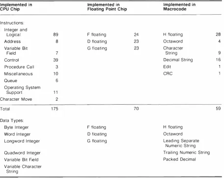
Reducing the Number of Transistors The pri ncipal problem in designing the 7 8 0 3 2 was how t o implement the complexity o f the VAX architecture on a single chip . There are 3 0 4 instructions in the ful l instru ction set, w i th 1 4 data types and 2 1 addressing modes. I nstruc tions vary in length from 1 byte to 54 bytes. 1
Dema n d - paged virtu a l memory s u pport is requ ired to guarantee compatibility with the operating system software . To accommodate this complexity in a ful l-scale VLSI VAX imple mentation requ ires about 1 . 2 5 million transis tor sites2 However, the semiconductor tech nologies available at the time of design could support only about one-tenth that number in a single-chip microprocessor.3
The architectural functions i n all VAX sys t e m s a r e p a r t i t i o n e d a m o n g h a r d w a r e , microcode, and the operating system . Al l previ ous VAX implementations have similar bounda ries between these three. The hardware pro vides the registers and memory, the microcode provides the instruction set, and the operating system provides the program services . A large contro l store-a minimum of 4 00 kilobits (Kb)
is requ i re d to c o n t a i n t h e i ns t r u c t i o n microcode . The console function is handled in either microcode or a support processor. More over, the control logic needed to support mem ory manage ment and the variable instruc tion format is quite complex4
Two d i fferent approaches were taken to reduce the transistor count in the microproces sor chip. First, the VAX instruction set was repartitioned to cut the size of the control store
Digital Technical journal
No. 2 Mm·cb 1986
to 62Kb . Second , the amount of on-chip hard ware was reduced by simplifying some func tions, placing others elsewhere, or omi tting some altogether.
Repartitio n ing the Instructio n Set
As the first repartitioning step, the design team assumed that all VAX instructions had to be implemented in order to execute all VAX appli cation software . However, there are several classes of i nstructions that involve a good deal of m ic rocode and yet are infrequently exe cuted. For example, a typical timesharing work load is handled by base instructions, scientifi cally oriented i nstructions , and commercially oriented i nstructions . Analyses of more than 70 mill ion executed i nstructions showed that the commercially oriented ones represented less than 0 . 2 percent of the total executed5·6 Stud ies of scientific and engineering workloads showed even lower percentages. Even in com mercial applications, the commercially ori ented instructions represented less than 4 per cent of the total executed , the majority being base instru ctions. Therefore , emu lating the commercially oriented instructions in the oper ating syste m rather than u s i ng m i crocode wou ld significantly reduce the size of the con trol store, but would have l ittle effect on over a l l performance because these i nstructions were seldom executed .
On the other hand, floating point instructions require a good deal of microcode and are exe cuted more frequently. Even with m icrocode, i nstruction execution is relatively slow unless a separate floating point accelerator (FPA) is used . Therefore, although existing VAX imple mentations offered both m icrocoded (warm) a nd hardware (hot) floating point , the design team decided not to implement these instruc tions in microcode . I nstead, floating point instructions wou ld be executed in an optional floating point chip, or by e m u lation using macrocode .
I n tota l , 1 75 of the 3 0 4 VAX instructions and 6 of the 14 data types are implemented in on chi p microcode . Those include integer and log ical instructions, variable-bit fie l d , contro l , queue, procedure calls, character string moves, and operating system support . This microcoded subset comprises over 9 8 percent of the instructions that are used to execute a typical program . H owever, the requ i red microcode
.--- The Micro VAX 78032 Chip, A 32- Bit Microprocessor
occupies only one-fifth the control store space of a fu l l VAX impl ementation. Seventy t1oating point instructions and three data types (F. D, and G t1oating) are implemented in the t1oating poinr chip, when it is present. If that chip is absent, the instru ctions are emu l ated i n macrocode . T h e remaining 59 instruct ions and
5 data types are a lways emu lated in macrocode. Those are main ly decima l string, character string, and H floating point operations . The CPU chip provides some microcode support for the emu lated instructions . Table 1 summarizes the instruction set arch itecture of the 78032 chip.
The decis ion to emu late instructions in macrocode has an effect on speed because emu lated instructions take three to ten times longer to execute than microcoded instructions . How ever, the instructions in this group of 59 a re
Table 1 Instruction Set Architecture
normally used so infreq uently that the execu tion speed of a typical program is reduced by no more than four percent. Tab le 2 i l lustrates the division of instructions between the CPU chip , the FPU chip, and the macrocode . All in all, the fivefold reduction in the size of the control srore ha lved what wou ld have been the active area of the chip .
Simplifying the Hardware Fu nctio ns
The principal hardware simp lifications in the 78032 are the reduced size of the address trans lation cache (translation buffer) , and the e limi nation of a memory cache in favor of tightly coupled local memory.
As mentioned earlier, demand-paged virtual memory management was requ i red for compati bi lity with the VAX architecture . Consequently, the design team decided that the 78032 woul d
Implemented i n CPU Chip
Im plemented i n Floating Point Chip
Implemented in Macrocode
In structions: I nteger and
Logical
Address Va riable Bit
Field
Control
Procedure Call
M iscellaneous Queue
Operati ng System
Support
Character Move
Total
Data Types:
Byte I nteger
Word Integer
Longword I nteger
Quadword Integer
Variable Bit Fie ld
Variable Character
String
14
89
8
7 39 3
10
6
11
2
175
F floati ng
D floating
G floating
F floating D floating G floati ng
24
23
23
70
H floati ng
Octaword
Character String Decimal String
Edit CRC
H floating Octaword
Leading Separate
Numeric String
Trai ling N u meric String Packed Decimal
28
4
9 16
59
[image:15.592.79.536.351.715.2]Table 2 Division of I nstructions
Percent by I n struction Count
Percent by Microword Count
Percent by Typical Execution Frequency
Instructions Implemented in CPU Chip
57.6%
20.0%
98. 1 %
be the first single-chip CPU with fu l l demand paged virtual me mory support right on the chip. At first the design team proposed to use a simp lified version o f VAX memory manage ment. During the course of the design , how ever, the software engineers reported that not providing fu l l memory management was quite expensive in terms of the use of p hysical mem ory. Therefore, the design team i mpleme nted fu ll VAX double-mapped compatibil i ty in the chip. As the design progressed, it became evi dent that the incrementa l cost of providing this capabi l i ty was much lower than orig i n a l l y anticipated .
Al l existing VAX processors implement mem ory management with a large address transla tion cache (at least 1 2 8 entries) , with system and process addresses in separate halves. A translation cache must have a high hit rate to be effective . Si nce most caches are direct mapped, many entries are requ ired to achieve a high cache rate 7·H Implementing a comparable num ber of translation cache entries in the 780 3 2 was out o f the question, due to die size con straints. However, the VLSI technology in the 780 3 2 is very amenable to using a fu l ly associa tive translation cache with least-recently-used
(LRU) replacement.
Such a cache needs many fewer entries to achieve the same hit rate as the d irect-mapped version. In add ition, the tight coupling to loca l memory, as explained i n the next paragraph, made i t poss ible to reduce drastica l l y the amount of time requ ired to process a transla tion cache miss . Thus the translation cache in the chip has only eight entries , but the cache is fu lly associative , uses true LRU replacement, a nd is su p p o r t e d b y h i g h l y o p t i m i z e d microcode for fast processing o f m isses.
More-Digital Tecbni<:al jourual
No. 2 /lfarch 1 ')86
Instructions Implemented in Floating Point Chip
23.0%
20.0%
1 .7%
Instructions Implemented in Macrocode
1 9.4%
60.0%
0.2%
over , simu lation studies showed that the best use of the eight entries was with a homogene ous structure . Therefore, the system and pro cess addresses are cached together .
The team also decided to forgo the use of an external memory cache, which requ ired a com plex external interface . Use of an internal mem ory cache had already been ruled out due to die size constraints. Accordi ngly, the speed of memory access is 400 ns, or two m icrocycles, which is the speed of local memory. Thus the chip encounters no wait states, and its average time to access memory is approximately the same as the 1 1 j780's. In a typical program , there is little difference between the i nteger instruction performance of the two CPUs .
Additional s i mplifications i ncluded the elim i nation of warm (microcoded) floating point in favor of a floating point accelerator , e l i m i na tion of wri table control store capabi l ity, and e l i m i nation of on-chip console su pport.
Design Narrative
The starting point for the chip design was the i nstruction execution chip of a multichip VLSI VAX processor already in design . This chip would provide a general floorplan and a base m i croarchi tecture , and might even provide complete design sections that cou ld be used for t h e M i c r o VAX 7 8 0 3 2 . As t h e p r o j e c t progressed, the designs o f the VLSI VAX proces sor and the MicroVAX 780 3 2 tended to d iverge under the pressure of differing constraints : chip set and system functionality for the former ; die size, power, and time to market for the latter . Ultimately, only part of the main datapath was s hared betw e e n the two ; the rest o f t he M icroVAX 7 80 3 2 design and i ts m icrocode were unique.
--- The Micro VAX 7803 2 Chip, A 3 2-Bit Microprocessor
The MicroVAX 780 3 2 project took 20 momhs from start to fi rst-pass mask generat i o n : 6 months for specification and general design, and 1 4 months for physical implementation . Eighteen people worked on the design ream .
Project Design Tools
The design ream was aided by a h ierarchica l CAD rool suite that ran on a VAX system. The use of these tools was one of the primary rea sons that the project was completed on sched u le . The principal components of t h is rool su ite are as fol lows :
1 . A proprietary chi p-database manager and tool i nterface called the CHAS system
2 . A schematic capture progra m , QUICK D RAW, t hat uses simple term inals
3 . A proprietary h i e rarch ical s i m u lator ca l l e d t h e DECS I M system , used for behavioral simulation
4 . A switch- leve l MOS logic s i m u lator, RSI M , used for u n i t-delay l ogic s i m u la tion
5 . A modified version of the standard SPICE circu i t simu lator that incorporates new ana lytica l, rather than empi rica l, MOS transistOr mode Is
6 . Design-rule checking programs, DRC and DRACULA I I
7 . A n i n te rcon nect verifica t i o n program cal led the IV system , which performs both layout extraction and wiring verifi cation9
8 . A cross-reference progra m , XREF, that ana lyzes c o u p l i n g , boots trap ra t i os , dynamic node stabi l i ty, and other c i rcuit problems
The chip layout was done on Calma GDS n systems. Three dedicated VAX- 1 1 /780 systems and five Ca lma stations were used throughout the project. The back-end verification of cir· cu i ts and the layout required as many as eight VAX systems .
Final Chip Design
The fina l product of this design process is a microprocessor that conta i ns 1 2 5 , 000 transis tOr s i tes in a 3 - micron , double-metal NMOS chip that measures 8 .7 by 8 . 6 m m . It requires
1 6
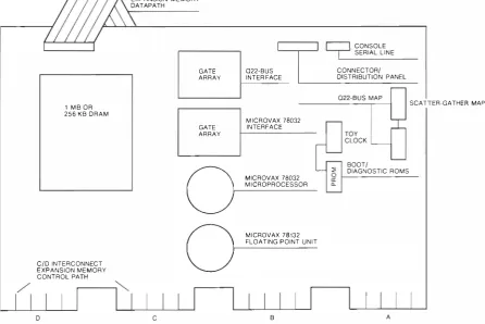
only 5 Vdc and a maxi mum o f 3 watts of power; it is pac kaged in a 68-p i n , su rface-mounted leaded chip carrier. The chip operates at 2 0 MHz and has fu ll 3 2 -bit i n terna l and external datapaths. The 780 3 2 is mounted on a s i ngle board , quad-si zed ( 8 . 5 by I 0 . 5 i n . ) CPU mod u le having a Q 2 2 1/0 bus and 1 megabyte (MB) o f loca l m e m o r y . An o p t i o n a l FPA, t h e M icroVAX 78 1 3 2 chip, can also be mou nred o n the CPU board .
The measu red speeds of integer and floating point operations of the 780 3 2 represent a breakthrough in 3 2-bit m icroprocessors . System evaluations of M icroVAX 780 3 2 modu les ind i cate that t h e i r performance in processi ng i nte gers is approxi mately equal to that of the VAX- 1 1 /780 system . With the floating point chip, the performance is between those of the VAX- 1 1 /7 5 0 and VAX- 1 1 /780 systems w i t h FPAs .
The remainder of this paper expla i ns the fu nctional organization of the chip and i ts phys ical i mplementation in silicon .
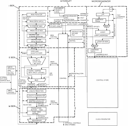
Functional Organization
The diagram i n Figure 1 and the photomicro graph in Figure 2 out l i ne the various subsec tions, or fu nctional boxes, of the M icroV AX 780 3 2 chip. They are organi zed i n to three sec tions . At the left of Figure 2 are the darapaths for decod ing and executing i nstructions and for memory management. At the center is the con trol logic for i nternal operations and the proto col signal logic for external operations. At the right is the sequencing l ogic for both internal and external operations.
The left sect i o n i n t h e p hotom icrograph ( Figure 2 ) , comprising the data paths, consists of the I Box, the E Box, and the M Box.
• The l Box prefetches and decodes instruc
tions. I ts main function is to parse the cur re n t macro i nstruct i o n in the i nstructi o n stream and work in conjunction with the mi crosequencer to generate t h e m icroad dress for the next mi cro instruction . This microaddress is a function of the current macroinstru ction . A prefetcher, which works i n para l l e l w i t h other c h i p opera t i o n s , accesses a n d stores instruction data i n a n eight-byte prefetch q u e u e . The prefetcher acts autonomously by atte mpting to keep that queue fu l l at all ti mes, using any free I/O-bus cyc les to access the i nstru ction
Digital Technical journal
INTERRUPT M I CROSEOUENCER
I BOX
...,_ "" •r - - - � - \
_j
JIN;,;R�-
�
� - - - - �- - --r--8-l ----,
r+---,---.---1 PRIORITY I
•
II
I
LEVEL Irl
READ ROTATORJ
Lr
INTERRuPT
1
,... .. pc r-L___.. TESTI
SYNCHRONIZERE
REO:
UES�S DATAPATH.l AN
D HALT I
L
,uADDRESSTOP BUS I INTERRUPT PRIOA1T1ZE R
POWER FAI L JtAOO RESS
Lr---H
REAO OATA LATCHI
L CONTROL - - - .-l STACK It _j INSTRUCTION (ENTAY·POINT .uADDAESSES)
�
UX�
ALIGNMENT Mux1
n oecooe LOGIC (�-tBRANCH oFFsET)t
I
! ,L...1 PREFETCH STACK
I'
I
1,--L---'.__,L...
r-1
�
I
NSTRUCT
I
ON
ADDER�-1
INSTRUCTION !BOX ,----'-....1...-, ��ODEI ,I
p OOR sSTREAM ROTATOR CONTROL
I
(JUM p.A E 51I
INSTRUCTIONI
MICROSEOUENCERI I
DATA REGISTER CONTROL I
I
1-'TRAP/OR BOXI
•
I I
�
L �
EBOX INPUT MUX_;-
jI
MUXI -
-n�·
- - - -r- - 1
I
I
,---p-:-:A0:-::D':::R:-:ES:-:S---,JI �
GPRS ANDJ-
LATCHB BUS SCRATCH PADS
I
I
I
I
p.ADDRESS BUSE BOX
I
�
I
Ly�-;.,-..-===-=�
--''N
\
ALU ,;;;ITHI
I
LATCH AND EBOX
I
:
I BIT SHIFT CONTROLI
rw-::R:::,T::-E---, I ROTATOR • �
I
I
AND �
I I
BARRELSHIFTER
I
Ig��e��
I wtTH INPUT lATCHES Aw MtCROtNSTAUCTtONEXTERNAL DATA AND ADDRESS BUS
I ---,
l
Bus 14---Bu_s_____.l._ ___ '--1I ---. t .--- CONTROL
I
INTE RNAL
\
MUXI
I
DATA AND
B
ADDRESS �
I
B� DRIVER
l�J_,
· - - - - _ ...Jr r--- - - -,
INPUT
L..
I
---1
LENGTH REGISTERSJ
I
DRIVERS [-I
•I
I
I
LENGTH COMPARATORJ
I
t
I
..___.j ADDRESS REGISTERSI
MBOXI
I
IWITH
INCREM ENTER CONT ROLI
TB/AW BUS
I
VIRTUALM sox,
I
• ADDRESS BUSII
f...J
I
TRANSLATIONI
I �I
BUFFER, TAGSI
PAGE TABLE
I
I
ENTRIESI
I
J
PHYS!CAL _JADDRESS BUS r -1 -1 ....--J \ .__M_U_X/-"D-R I-VE-R--,/
I
L.. _ _ -.- _ _ J I EXTERNAL CONTROLS
t AND STROBES
Figure 1 Block Diagram of the CPU Chip
CONTROL STORE
CLOCK GEN ERATOR
strea m . Even i f t h e q u e u e is fu l l , the prefetcher will start to read data if the queue will be at least half-empty after the current microcycle.
The l Box a lso decodes i nstructions and vari able-length operand specifiers in para l lel with other chip operati ons . That avoids requ iring explicit decode cycles to execu te successive macroinstructions . Due to the constraints on the size of the control store, most of the address-specific microcode had to be shared among a l l instructions. The
i nstruction-decode PLA (lPLA) generates 1 9 bits of opcode-specific data for controlling other chip operations related to a giv e n instruction . That a l l ows many microcode sequences to be table driven and shared.
DigiUll Technical journal
No. 2 March 1986
• The E Box is the instruction execu tion unit and contains the main datapath of the chip. This box holds 1 6 VAX-specified genera l pu rpose registers (GPRs) , 20 microcode reg isters, a 3 2-bit arithmetic logic unit (ALU) , and a 3 2 -b i t barrel shifter. The E Box a lso maintains condition codes for t he process
[image:18.591.73.506.88.514.2]The Micro VAX 78032 Chip, A 3 2-Bit Microp1·ocessor
1 8
t. -:... -�.,.:-- --..
-I
t
I
.
.-
�
.' .. .. . · t., · J · I I---'"� .J .,,_ .
I "' - t • •.: :
�
• I I .. I
Figure 2 Photomicrograph of the CPU Chip
status longword (PSL) and determi nes VAX branch conditions at the macrocode level . In a 200-ns cycle , the E I3ox can read two regis ters , perform an ALU operation or shift, and write the result into a register. Si nce reading a n d writing to regis ters are performed sequentially, the ALU result bus is mul tiplexed with an i nput bus. thus saving vert i cal interconnect . The ALU employs a 4 -bit
lookahead carry sche me, with ripple carries across the nibbles . The carry chain uses dual rail logic for maxi mum speed . The barre l shifter is a pass-transistor network, which is very compact and fast enough for this task.
• The M I3ox serves as the memory ma nage
ment unit and translates vi rtual addresses to physical addresses. The address translation cache , which is ful ly associative, stores t he most rece ntly referenced address transla tions. The M I3ox maintains three virtual address registers , one for instruction data and two for program data. This unit also detects cross-page accesses and includes a separate compararor for length checking. A dedicated adder generates the next vi rtual address for seque ntial data and instruction addresses . The time to perform an add ress translation is less than 2 5 ns when the virtua l address is i n
[image:19.592.93.535.92.513.2]the translation cache . This short translation time a l lows memory management to be trans parent to the external chip timing.
The center section of the photom icrograph is composed mostly of random control logic. That logic translates the highly vertical ( 3 9 - bit) microcode into the many discrete control sig na ls requ ired to operate the datapath .
The right section of the photomicrograph, comprising the sequencing and clock ing logic, consists of the inte rrupt logic, the control store , t h e DAL interfa c e , and t h e c l oc k generatOr.
• The interrupt logic accepts , synchronizes, and prioritizes external interrupt requ ests, compares them with the current interrupt priority leve l (IPL) , and determines if the request w i l l be s e rv i ce d . T h e interrupt requ ests are c hecked at the beginning of each microcycle and the interrupt update is forwarded to the I Box . That all happens through the central control logic before the next microcycle begins .
Exte rna l interrupt processing has been implemented on-chip in the 78032 to avo id the complex ity that results from having the interrupt priorities arbitrated outside the chip. Since these priorities are an integral part of the processor state, an off-chip design wou ld invo lve broadcasting the interrupt priority level eac h time it changed . More over, off-chip interrupt processing wou l d also require additional hardware o n t h e C PU board .
• The microsequencer accepts inputs from various points on the chip and generates the next microaddress to access the contro l store . The microsequencer logic pe rforms such operations as microsubroutine calls and returns, microcode traps, n-way (or case) branches , and s i gned offset cond it ional branc h e s . I m pl emented in the m i c rose quencer is an e ight- level m icroprogram stack.
• The control store is a 3 9 -bit ROM with 1 6 00 entries . It receives microaddresses and status s ignals and generates the next set of microin structions . The control store transfers those microinstructions to the control section in the center area . That section , in turn,
gener-Di�ital Tecbnica/ journal
No. 2 Manb I ')8()
ates control signa ls for the three principal functions in the main datapath : the I Box , the E Box , and the M Box. The access time of the control store is less than I 00 ns .
• The DAL interface handles a l l control signals and transfers data and addresses between the chip and local memory, peri pherals, and other devices outside the c h i p . The DAL interface transparently processes variable length operands and al igns data references that cross natural 3 2 -bit memory boundaries. It also causes the microprocessor to sta l l dur ing r;o referenc e s , so t h at add i t i ona l microcode is not needed tO test for I/0 com pletion. The DAL interface contro ls transac tions involving the C PU chip, the FPU chip, and externa l devices. It also a rbitrates direct memory access (DMA) requests .
• The clock generatOr receives an externa l 40 -MHz c lock reference and produces the eight 2 5 -ns clock phases that time functions on the chip . The control logic of the chip makes extensive use of bootstrapped drivers . For that reason, certain clock phases have to drive very high capac itances, as much as 2 5 0 picofarads . To assist in that task, a special driver c ircu it with cu rrent- l i m iting resistors is used to provide fast edges without using excessive power or silicon area. These resis tors control the overlap cu rrent drawn d u r ing bootstrapping and provide a voltage drop during the overlap.
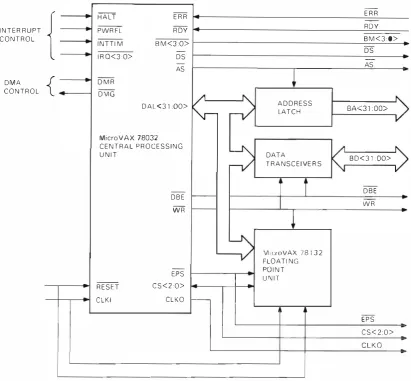
External Interface
A principal goa l in designing the chip's exter nal interface (Figure 3) was to demand as few support functions as possible from the CPU board . The 7 8 0 3 2 chip provides seven hard ware interrupt inputs . Fou r of these inp uts
(IRQ<3 : 0> L) correspond to standard VAX I/0 interru pts and res u l t in vectored interrupt transacti ons . Three others (I NTTIM L, PWRFL L, HALT L) have preassigned interpretations and the corresponding vectors are generated inside the chip. The 7 8 0 3 2 takes in a double-fre qu ency clock input from a standard oscil lator. The chip produces a normal-frequ ency clock output, which can be used to drive or synchro nize external logic. The functions between the chip and the Q-bus can be implemented in off the-shelf discrete logic .
--- The Micro VAX 78032 Chip, A 32-Bit Microprocessor
I N T E R R U P T C O N T R O L
D M A C O N T R O L
{
{
H A LT
PWR F L
--I N T T --I M
I R Q < 3 0>
--D M R
--D M G
-E R R E R R
- R O Y
R OY
B M < 3 :0> B M < 3 O>
- D S
D S
- AS
AS
�
/"
�
A D D R E S S D A L < 3 100>Y--
r-V
LAT C H BA<3 1 : 00>M i c ro V A X 78032
C E N T R A L P R O C E S S I N G
�
�
8 0 < 3 1 : 00>U N I T DATA
r-V
T R A N S C E I VE R S- D B E
O B E
-- W R
W R
-�
�
M 1 cr0VAX 7 8 1 3 2F L O A T I N G
- PO I N T
EPS
U N I T
--R E S E T C S < 2 0 >
C L K I C L K O
r--E P S
C S < 2 : 0 >
C L K O
Figure 3 External Interface
E xcept for the 3 2-bit DAL bus , the external interface closely resembles t hose for existing 1 6-bit microprocessors . Specifical ly, its timing and signal complement are quite similar tO those in current machines . The addresses and data on the DAL are time division multi plexed, with separate timing strobes (AS and DS, respec tively, in Figure 3) . The data direction and the data buffer signals (WR and DBE in Figure 3) are used to control exte rnal transcei ve rs directly. The cycle status signals differentiate among the various types of bus transactions . Four-byte mask signals , one for each group of eight bits on the DAL bus, allow straightfor ward manipulation of bytes within longwords
(four bytes) .
2 0
The ROY signal a l l ows slower peri p heral devices on the I/0 bus to stretch the me mory access time beyond 4 0 0 ns until they are ready tO respond .
Parallel Opera tio n
Besides giving the 780 3 2 opti mized microcode and a fast microcycle time, the design team en hanced the chip's performance by allowing parallel operations between and within func ti onal subsections. This parallel flow is actually a form of pipel ining in which the operations happen independently a nd concurre ntly. For e xa m p l e , w h i l e the E Box is execut i n g a datapath operation, the control store can access the next microinstruction . At the same time , the
[image:21.592.96.508.99.480.2]microsequencer can be calculating the add ress of the microinstruction after that one, and the M Box can be trans lating a virtual ad dress . Meanw h i l e , the I Box can be decoding an instruction or operand specifier and prefetch ing more instruction data . And the DAL inter fa ce can be i n i ti a t i n g or c o m p l e t i n g a n external bus operation .
For example, assume that the chip is tO exe cute the fo l l owing two t h r e e - m icro cyc l e macroinstructions i n sequence :
ADDL3 RO, R l , R2
SUI3L3 R4 , R S , R6
Withi n the thi rd 2 0 0-ns microcyc!e, some operations associated with these two macroin structions are performed in parallel by several subsections. The E Box will write the resul t of ADDL3 into R2 in the register fil e , set the PSL condition codes, and check for arithmetic exceptions, such as an overflow trap. Mean while, the I Box w i l l decode the next macroi n struction , SUBL3 , and its first specifier, R4 . Concurrently, the prefe tcher in the I Box will determine i f the decode of the instruction and specifier w i l l c le a r e n o u g h space i n t h e prefetch stack t O warrant another longword transfer. If so, the I Box will then initiate the transfer and fetch another macroinstruction, which also involves the DAL interface .
Within each subsection, there are a lso a num ber of parallel operations that reduce the over all execution speed significantly. In addition tO simultaneous prefetch and decode actions in the I Box (as described above) , the microcode access in the control stare is pipeline d : The next microaddress is accessed while the current microinstruction at the current microaddress is being executed . In the M Box, length checks against referenced addresses take place simulta neously with the translation cache l ookups . If a lookup misses , therefore, the length check will have already determined whether or not the ref erenced page is within range . In the E Box, a separate program counter ( PC) adder maintains the PC so that the ALU can be dedicated to its primary tas k.
Some typical execution times for instructions u nder normal operating conditions (al igned operands, no memory management exceptions) are as fol lows :
Digital Technical journal No. 2 March 1986
Typical
Execution Time In struction Operands (Nanoseconds)
MOVL Reg , Reg 400
ADDL2 Reg , Reg 400
MOVL Mem, Reg 800
A D D L2 Mem, Reg 800
MOVL Reg , Mem 600 A D D L2 Reg , Mem 1200
Conditional 200
Branch ,
not taken
Conditional 800
Bra nch,
taken
Physical Implementation
The MicroVAX 780 3 2 chip is made using a 3-micron, double -meta l NMOS process that a llows power savings and superior circuit flexi bility . Until the MicroVAX 7 8 0 3 2 chip design, single metal was a standard for NMOS technol ogy. The use of a second layer on the 7 8 0 3 2 c h i p was a significant departure for NMOS design . There are two main advantages of a double-metal implementation . First, it is easier to place logic circu its in the interconnect layer, where there are more circuits per u nit area of silicon . Second, the metal interconnect has lower resistance than polysilicon, thus avoiding wire delays that are difficu l t to elim inate in design .
The double-metal process provided the chip design team with two layers of alu minum inter connect and fou r types of devices (N, E, L, and D) . The four types allow some savings in power and a substantial i ncrease in circuit flexibility. However , the E device ( l ight enhancement) is typical l y used only in source-follower circuits, and the L device ( l ight depletion) only in latches and stati c memories . The second layer of aluminum interconnect manages the com plexity associated with 3 2 -bit microprocessors . That p e r m i t s g l o b a l c o m m u n i c a t i o ns a n d a llows local control or routing to share the same chip area. H owever, second metal can only contact first meta l , and then only through an offset, or staggered, contact.