Digital Equipment Corporation
Maynard, Massachusetts
Reference Manual
;1
PDP-15 Systems
DEC-15-BRZA-D
PDP-15
1 st Printing August 1969
Copyright
©
1969 by Digital Equipment CorporationInstruction times, operating speeds and the like are in-cluded in this manual for reference only; they are not to
TABLE OF CONTENTS
Chapter Page
General Description
Introduction 1-1
PDP-15 Highlights 1-1
Summary of PDP-15 Characteristics 1-2
2 PDP-IS System Organization
Central Processor 2-1
Memory 2-1
I/O Processor 2-1
System Peripherals 2-3
3 Organization of the Central Processor
Summary of Characteristics 3-1
Central Processor Description 3-1
Processor Expansion 3-4
4 Memory Organization
Summary of Characteristics 4-1
Core Memory 4-1
5 Organization of the Input/Output Processor
Summary of Characteristics 5-1
I/O Processor 5-1
Addressable I/O Bus 5-7
Program Interrupt Facility 5-9
Automatic Priority Interrupt 5-10
Common I/O Bus 5-12
IOP1, IOP2, IOP4 5-13
6 Addressing
Interpretation of Words From Memory 6-1
Information Retrieval From Memory 6-1
Memory Reference Instructions 6-2
Bank Mode Addressing 6-5
Nonmemory Reference Instructions 6-5
Operate Instructions 6-5
Data Words 6-6
Basic Software Floating-Point Formats 6-7
TABLE OF CONTENTS (cont.)
Chapter Page
7 Instruction Repertoire
Instruction Groups 7-1
Transfer Instructions 7-3
Arithmetic Instructions 7-3
Logical Instructions 7-4
Rotate Instructions 7-S
Control Instructions 7-S
Jump Instructions 7-7
Index and Limit Register Instructions 7-9
Register Control Instructions 7-10
Microcoding 7-11
Input/Output Instruction Group 7-13
8 Internal Options Instruction Set
EAE 8-1
Basic Shift Instructions 8-4
Normalize Instructions 8-6
Arithmetic Instructions 8-7
Automatic Priority Interrupt Instruction Set 8-13
Memory Parity 8-lS
Real-Time Clock 8-16
Power Failure 8-16
Memory Protection Option 8-17
Memory Relocation and Protect KT IS 8-19
The Hardware 8-21
9 Peripheral Options
Standard Input/Output Devices 9-1
Mass Storage Devices 9-1
Line Printers and Plotters 9-3
Data Communications Devices 9-3
Display Devices 9-4
Interprocessor Buffer Systems 9-S
Analog-to-Digital Converters 9-S
Digital-to-Analog Converters 9-6
Operational Amplifier, Type AH03 9-6
I/O Bus Adapter, Type DWIS 9-6
10 PDP-IS Console
Information/Control Switches 10-1
Operate Control Switches 10-3
Special Switches 10-4
TABLE OF CONTENTS (cont.)
Chapter Page
11 System Software
Appendix
PDP-15/10 Compact Software System PDP-15/20 Advanced Monitor System Common PDP-15 Software
PDP-15/40 Disk-Oriented BACKGROUND/FOREGROUND System Additional Systems Software
Diagnostics
A Installation Planning Physical Configuration Placement of Options
11-1 11-2 11-3 11-7 11-7 11-9
~.
INSTALLATION MANUAL
MODULE MANUAL
HARDWARE ACCEPTANCE
TE ST PROCEDURES
INTERFACE MANUAL
PDP-15 FAMILY OF MANUALS
OPERATORS GUIDE
SOFTWARE
MACRO -15
FOCAL -15
UTILITY PROGRAMS
MANUAL
FORTRAN nz::
8/15 TRANSLATOR
-<
.-. .
.-..
SYSTEM REFERENCE MANUAL - Overview of PDP-15 hardware and software systems and op-tions; instruction repertoire, expansion features and descriptions of system peripherals.
USERS GUIDE VOLUME 1, PROCESSOR -Principal guide to system hardware includes sys-tem and subsyssys-tem features, functional descrip-tions, machine-language programming consider-ations, instruction repertoire and system expan-sion data.
VOLUME 2 PERIPHERALS - Features function-tiona I descriptions and programming consider-ations for peripheral devices.
OPERATOR'S GUIDE - Procedural data, includ-ing operator maintenance, for usinclud-ing the oper-ator's console and the peripheral devices asso-ciated with PDP-15 Systems.
PDP-15/10 SYSTEM USER'S GUIDE - COM-PACT and BASIC I/O Monitor operating proce-dures.
PDP-15/20 SYSTEM USER'S GUIDE - Advanced monitor system operating procedures.
PDP-15/30 SYSTEM USER'S GUIDE - Back-ground/Foreground monitor system operating procedures.
PDP-15/40 SYSTEM USER'S GUIDE - Disk-oriented background/foreground monitor system
PDP-15/10 SOFTWARE SYSTEM - COMPACT software system and BASIC I/O Monitor system descriptions.
PDP-15/20 ADVANCED Monitor Software Sys-tem - ADVANCED Monitor SysSys-tem descriptions; programs include system monitor and language, utility and application types; operation, core or-ganization and input/output operations within the monitor environment are discussed.
PDP-15/30 BACKGROUND / FOREGROUND Monitor Software System - Background/Fore-ground Monitor description including the asso-ciated language, utility and applications pro-grams.
PDP-15/40 Disk-Oriented BACKGROUND/ FOREGROUND Monitor Software System -Background/Foreground Monitor in a disk-ori-ented environment is described; programs include language, utility, and application types.
MAINTENANCE MANUAL VOLUME 1, PRO-CESSOR - Block diagram and functional theory of operation of the processor logic. Preventive and corrective maintenance data.
VOLUME 2, PROCESSOR OPTIONS - Block diagram and functional theory of operation of the processor options. Preventive and corrective
VOLUME 3, PERIPHERALS (Set of Manuals) -Block diagram and functional theory of operation of the peripheral devices. Preventive and correc-tive maintenance data.
INSTALLATION MANUAL - Power specifica-cations, environmental considerations, cabling and other information pertinent to installing PDP-15 Systems.
ACCEPTANCE TEST PROCEDURES - Step-by-step procedures designed to insure optimum PDP-15 Systems operation.
MODULE MANUAL - Characteristics, specifica-tions, timing and functional descriptions of mod-ules used in PDP-15 Systems.
INTERFACE MANUAL - Information for inter-facing devices to a PDP-15 System.
UTILITY PROGRAMS MANUAL - Utility pro-grams common to PDP-15 Monitor systems. MACRO-15 - MACRO assembly language for the PDP-15.
FORTRAN IV - PDP-15 version of the FOR-TRAN IV compiler language.
PDP-IS Systems offer comprehensive solutions to real-time data problems. They combine new design concepts with a wide array of traditional features that spring from Digital's years of leadership in the medium-scale scientific com-puter field. Both elements share the common purpose of simplifying the user's tasks in a demanding real-time environment.
Since certain types of data-handling tasks re-quire specific hardware and software configura-tions, Digital has developed four standard PDP-IS Systems, ranging in power from the modestly priced basic PDP-IS / I 0 to the real-time disk monitor environment of the PDP-IS/40. At every level, the capabilities of the hardware are under the control of a monitor designed specifically for them.
The software systems were designed around the hardware with the user environment in mind. The principal design objectives were to provide (a) a system that is convenient for the user to implement and that affords the user access to the full power of the hardware, (b) a system that allows the user to easily integrate his
appli-FOREWORD
cations programs and special peripheral device handlers without forcing him to become a sys-tems programmer and (c) a system that can expand naturally with any additional hardware the user purchases. PDP-IS Systems software allows the user to move from a very basic machine to a sophisticated system environment without the cost and complication of repro-gramming at each upward step.
I
SYSTEM DESCRIPTIONS
PDP-IS/1O: Basic System
The PDP-IS
II
0 is the first level PDP-IS System. The system's design provides limited budget users access to the power, speed, and 18-bit word length of PDP-IS hardware, in the expec-tation that the system can later be expanded to take full advantage of the advanced software capabilities inherent in the system's design.Hardware includes 4,096 18-bit words of core memory and a Model ASR33 Teletype console teleprinter. The system has the rapid PDP-IS 800-ns memory cycle time which provides 1.6-Ms add capability. Facilities for later expansion are prewired into the system; additional memory and peripherals can be plugged in as they are required.
Software is governed by the COMPACT Pro-gramming System, a complete package including Assembler, Editor, Octal Debugging Technique, and mathematical and utility routines. All are designed to function in a 4096 word system. The software offers complete upward compati-bility at the source level and field-proven relia-bility. Programs written for execution under COMP ACT may also run, with little or no modification, within all PDP-IS system levels up through PDP-IS/30 and PDP-IS/40 BACK-GROUND/FOREGROUND systems.
PDP-IS/20: Advanced Monitor System
PDP-IS/20 is an 8,192-word mass storage ori-ented system designed for research and engineer-ing environments where real-time data acqui-sition and control tasks are combined with program development and testing.
Program development, debugging, and modifi-cation are all handled under monitor control, virtually ending intermediate operations. Unique real-time input/output routines can also be in-tegrated into the system monitor to accelerate set-up and recovery.
Users are spared the task of writing system software to handle input/outputs to all standard system peripherals, since appropriate routines are supplied with the monitor. The net result is that even inexperienced computer users can get their applications programs "on the air" in a minimum of time.
PDP-IS /20 hardware facilities include not only 8,192-words of core memory and high-speed paper-tape facilities but also a DECtape control unit and two tape transports for convenient mass-memory storage. DECtape is Digital's com-pact, inexpensive answer to the problems of program and data storage. A single pocket-sized reel of tape can accommodate up to ISO,OOO words of information. The extra-heavy duty K S R 3S Teletype unit is included in the PDP-IS/20 configuration to guarantee a high degree of reliability under the strain of con-tinued heavy use. Also included is the extended arithmetic element described in Chapter 3. This unit facilitates high-speed multiplication, divi-sion, shifting, normalization, and register mani-pulation.
The IS /20 Advanced Monitor System provides not only mass-memory supervisory control but also complete device independence, so that pro-grams need not be limited to the use of certain specified input/output devices. Simple I/O state-ments control data handling; and the selection of physical devices is determined at run time on the actual machine, not when the program is written. This system also allows for easy integra-tion of real-time I/O level subroutines as new devices are added.
The Advanced Monitor permits two types of user interaction. These are (a) batch processing for routine production jobs and (b) keyboard interaction so that the user operates the system with simple commands typed at the keyboard.
Other Advanced Monitor features which utilize processor options, include a real-time clock con-trol and a priority interrupt concon-trol.
have a single aim: to make the system as approachable as possible to users who want "hands-on" interaction, yet as automatic as possible in terms of taking care of routine elements in programming.
PDP-15/30 BACKGROUND/ FOREGROUND System
The PDP-I 5 /30 System was designed to meet the demands of research, engineering, and industrial environments, where one or more real-time tasks typically require continuous re-sponsiveness from the computer but do not use
100% of its capacity.
Under the control of the PDP-I5/30 BACK-GROUND/FOREGROUND Monitor, real-time tasks are handled in the computer foreground and have immediate call on the system's re-sources via interrupts. Background time (time left over between service calls for the real-time tasks) is available for program development and testing or other lower priority computation.
The PDP-15/30 Background/Foreground system contains 16,384 words of core memory and all the devices standard for the PDP-I5/20. In addition, PDP-I5/30 Systems are equipped with a memory protect system, a real-time clock, automatic priority interrupt, a third DECtape transport and a second on-line teletype for background use.
The Background portion of the PDP-15/30 System encompasses the Advanced Monitor functions and capabilities: Macro assembler (MACRO-15), FORTRAN IV, FOCAL-15, EDIT, DDT (Dynamic Debugging Technique), DUMP for off-line debugging, PIP-15 for in terdevice file transfers, S-GEN (System Generator), link-ing and loadlink-ing, and interactive file access. In addition, the BACKGROUND/FOREGROUND Monitor contains all the supervisory controls
necessary for concurrent processing of back-ground and foreback-ground tasks.
In addition to the Advanced Monitor programs and routines, PDP-I5/30 users (and all other PDP-I5 system users) can draw on the consider-able program library and applications knowledge of DECUS (the Digital Equipment Computer Users Society), the second largest and most active computer users' group in the world. DECUS members share in the exchange of pro-grams a nd technical papers at regularly scheduled meetings throughout the year. Pro-ceedings of society meetings are published and distributed to members under Digital sponsor-ship.
PDP-15/40 Disk-Oriented BACKGROUND/ FOREGROUND System
PDP-I5/40 Disk-Based Background/Foreground System fulfills the demands of industrial and engineering environments where the need for a background/foreground mode of operation is compounded by the necessity for large random-access files.
The PDP-I5/40 System with 24,576 words of core memory, high-speed paper"tape facilities, and DECtape storage, also incorporates a DEC-disk control and two random access DECDEC-disk files. The two disks, whose storage capacity of 524,288 18-bit words can be expanded to 2,097,152 words, permit high-speed overlays chaining and system and user loading.
Other hardware features of the PDP-I5/40 in-clude a memory protect system, background Teletype and a real-time clock.
INTRODUCTION
Digital Equipment Corporation's PDP-IS Sys-tems are 18-bit fixed word-length, general pur-pose, binary digital computers. These systems are highly reliable, flexible, and complex tools which, together with their monitor systems and line of peripherals, can be used to help solve such diverse problems as data acquisition, pro-cess control instrumentation, scientific computa-tion and man-machine communicacomputa-tions.
This manual furnishes the reader with enough background information to familiarize himself with the PDP-IS System's present and potential capabilities.
PDP-IS HIGHLIGHTS
Complete System Autonomy
The basic PDP-IS System has an organization consisting of three autonomous subsystems Central Processor, Memory, and I/O Processor -each with independent timing and control logic. Communication between these subsystems is
CHAPTER 1
GENERAL DESCRIPTION
accomplished through the use of an effective, asynchronous, request scheme. This subsystem autonomy facilitates wide-scale expansion of the system, increased throughput, high capacity, re-liability and maintainability. With this approach, there is no concern about obsolescence; new subsystems incorporating the latest develop-ments in computer technology can be added readily, without affecting either program com-patibility or the operation of other subsystems.
Central Processor Autonomy - The full
capa-bility for controlling and executing the stored program is centered in the system's Central Processor. The Central Processor, by virtue of its control autonomy, coordinates its own opera-tion with that of other subsystems, thus pro-viding supervisory control over the PDP-IS.
The basic processor includes a number of major registers for processor-memory communications, a program counter, an accumulator, an index register and a limit register. Two 18-bit registers are used for memory buffer functions. This allows for processor overlap with memory cycle time, and effects faster instruction execution times.
Memory Autonomy - Independent read/write
control and buffer logic in each memory bank establishes complete autonomy for the memory. This means that memories of different cycle times can be used together, and also provides for the expansion beyond 32,768 words.
Input/Output (I/O) Processor Autonomy - The
I/O Processor has prime responsibility for con-trolling intercommunications between external system devices and the PDP-IS Memory or Central Processor. This third autonomous sub-system of the PDP-IS System contains eight data channels which may use either single-cycle block transfer devices or multi-cycle devices. The I/O Processor also contains an addressable I/O bus and provisions to add a real-time clock and an automatic priority interrupt system. The I/O Processor operates in parallel with the system's Central Processor and grants external devices access to PDP-IS Memory through the single- or multi-cycle data channels.
Real-Time Capabilities
The unique combination of a powerful processor and a very fast autonomous I/O section with such real-time features as an 8-level, 32 channel, automatic priority interrupt system coupled with a range of monitor systems, gives the user exceptional real-time capabilities on his PDP-IS.
System Reliability
To ensure system reliability, options such as power fail detection, memory relocation, mem-ory protection and memmem-ory parity are all avail-able on the PDP-IS System.
Hardware Reliability, Maintainability and Low Cost
A combination of such engineering considera-tions as worst-case design criteria for propaga-tion delays, over-voltage and over-current pro-tection, point-of-load regulator cards, minimal cable lengths, and extensive control panel (where twenty-four 18-bit groups of signals can be displayed including all major registers and buses), proven TTL logic, single time-state stepping and automatic checkout procedures provide the PDP-IS with two key characteristics.
It is an extremely reliable and easily maintain-able digital computer.
SUMMARY OF PDP-IS CHARACTERISTICS
Description - Programmed Data Processor - fixed
18-bit word length, parallel mode, autonomous operation, TTL circuitry.
Instruction List - Five basic instruction groups:
Memory Reference Operate
Input/Output Transfer Register Control/Transfer Extended Arithmetic Element
Core Memory - 800-ns magnetic core memory
expandable to 32,768 words; expansion with 4096 word pages or 8192 word memory banks; independent bank read/write control; provision for expansion beyond 32,768 words to 131,072 words built in.
Fixed Point Arithmetic (J's and 2's Comple-ment) - 18-bit ADD in 1.6 J1S 18-bit multiply* in 7.0 J1S, 18-bit divide* in 7.2S J1S.
Addressing - Single level indirect addressing;
direct addressing to 4,096 words, indirect ad-dressing to 32,768 words, indexed to 131,072 words. In bank mode, direct addressing to 8,192 words and indirect to 32,768 words.
Indexing - 1 index register, 8 auto-increment locations.
Input/Output - Up to 8 bidirectional channels communicating directly between the I/O bus and memory; addressable I/O bus normally ser-vices up to 42 device controllers.
Interrupt System - Basic machine has one pro-gram interrupt line. As an option there is an 8-level (4 hardware and 4 software) 32-channel Automatic Priority Interrupt that is expandable to eight devices per hardware leveL priority can be changed dynamically under program control.
System Console - Includes facility to display twenty-four l8-bit groups of signals including all major registers and buses of the processor and I/O section. These displays provide both pro-gramming and maintenance information.
Non-Existent Memory Trap - Accessing non-existent memory is sensed by a timer performing a watch-dog function. The user is informed of such errors through an API (level 0) or PI interrupt.
Real- Time Clock - Core location 00007 can be incremented by a user determined frequency. The real-time clock interrupts control the CPU when location 00007 overflows.
Peripheral Equipment - Includes paper-tape sta-tion, card readers, line printers, magnetic tape controllers, disk systems, displays, processors, A/D and D/ A equipment and communications equipment.
Options - Extended Arithmetic Element. Power Fail, Memory Protection, Memory Parity, Mem-ory Relocation, Real-Time Clock, Automatic Priority Interrupt system.
Operating Environmental Specifications
Equipment Temperature Relative Humidity
Processor 00 to 500C 10% - 95%
Typical System
*
100 to 350C 25% - 75%*Inc1udes paper tape station, card reader, magnetic tape, line-printer, etc.
Power Requirements
Voltage (AC) Frequency (Hz) Current Average
(± 15%) (±2 Hz) (A)
100 50 33
115 50 30
200 50 18
215 50 17
230 50 16
120 60 29
240 60 16
NOTE
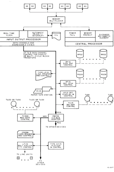
Three autonomous subsystems - Central Proces-sor, Memory, and I/O Processor - operating together under console control define the PDP-IS System. Coupled to the PDP-IS I/O Processor and serviced under the jurisdiction of the Monitor systems, an extensive line of peri-pherals including mass storage, displays, data communications and data acquisition equipment combine to form the PDP-IS System. Figure 2-1 illustrates the relationship of each computer subsystem and the peripherals to the entire complex.
CENTRAL PROCESSOR
The Central Processor functions as the heart of the computer by carrying on bidirectional com-munication with both Memory and the I/O Processor. Provided with the capability of per-forming all required arithmetic and logical op-erations, the Central Processor plays the major role in the control and execution of the stored program. It accomplishes this with an extensive complement of registers, control lines and logic gates.
CHAPTER 2
PDP-15 SYSTEM ORGANIZATION
MEMORY
The Memory, second of the three autonomous subsystems, is the primary storage area for com-puter instructions and system data. Memory is organized into pages which are paired into mem-ory banks. Each page has 4096 l8-bit binary words of high-speed random-access magnetic core storage. Each bank is an asynchronous unit of 8192 words; expansion capability to 32,768 words (four banks) is provided for each PDP-IS System. Any word in Memory can be addressed by either the Central Processor or the I/O Processor. The CPU has provisions to address up to 131,768 words of core memory. The autono-my of the memory system allows mixing banks with different cycle times.
I/O PROCESSOR
REAL TIME CLOCK
AUTOMATIC PR lOR I T Y INTERRUPT
INPUT OUTPUT PROCESSOR
DATA CHANNELS AND ADDRESSABLE lIO BUS
TU20 OR TU30
UP TO 8 DATA CHANNEL CONTROL FOR SINGLE-OR MULTI-CYCLE BLOCK TRANSFERS
~
PAPER TAPE STATION TU20 OR TU30
9 ...
L _ _ _TO LI N E UN ITS
TO OTHER DEY ICES
TO OTHER DEVICES POWER
FAIL EXTENDED ARITHMETIC
ELEMENT
CENTRAL PROCESSOR
~
I_ _ --.J
e
R
_ -.l
TU55
.... .. Q
---~
15· 0017
Figure 2-1. System Organization
[image:20.612.134.508.83.648.2]..
Single cycle block data transfer; blocks of data transfer at rates up to one million words per second.
Multicycle block data transfer; blocks of data transfer at rates up to 250,000 words per second for input and 181,000 words per second for output.
Program controlled data transfers; single word transfers to/from the accumulator in the Central Processor
The I/O Processor provides timing, control and data lines for information transfers between memory or the Central Processor and the
periph-eral devices, it also includes provision for such options as the Automatic Priority Interrupt Sys-tem and the Real-Time Clock.
SYSTEM PERIPHERALS
The PDP-IS System Peripherals range from sim-ple input/output Teletypes to sophisticated in-teractive display processors. These peripherals communicate with the PDP-IS I/O Processor via one 72-wire bidirectional cable called the com-mon I/O bus.
..
CHAPTER 3
CENTRAL PROCESSOR ORGANIZATION
SUMMARY OF CHARACTERISTICS
Description - 18-bit parallel operation,
autono-mous operation, fixed-point signed and unsigned arithmetic (l's and 2's complement)
Instmction Types
-Memory Reference Operates
Register Transfer and Control Extended Arithmetic Element Input/Output Transfer
Indexing - 1 index register, I limit register, 8
auto-increment locations
Timing
-Typical Instructions 18-bit ADD 18-bit Multiply* 18-bi t Divide* 36-bit Shift* 36-bit Normalize*
*With EAE
Execute Time
1.6 J.l.s
7.0 J.l.S
7.25 J.l.S
7.25 J.l.S
7.25 J.l.S
CENTRAL PROCESSOR DESCRIPTION
The Central Processor (CPU) is the nerve center for control and execution of stored programs. By coordinating its own operation with that of other subsystems, it provides supervisory control over the PDP-IS System.
The Central Processor contains arithmetic and control logic hardware for a wide range of operations. These include high-speed fixed-point arithmetic with a hardware multiply and divide option, extensive test and branch operations implemented with special hardware registers, high-speed input/output instructions and other arithmetic and control operations.
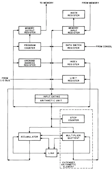
The PDP-IS Central Processor contains several major registers for processor-memory communi-cations, a program counter, an instruction regis-ter, an accumulator, an index regisregis-ter, and a limi t register.
instructions work are stored in the core memory of the PDP-IS. The arithmetic and logical opera-tions necessary for the execution of all instruc-tions are performed by the arithmetic unit oper-ating in conjunction with central processor regis-ters. Figure 3-1 shows a simplified block diagram of the Central Processor.
Arithmetic Unit (AU)
The PDP-IS arithmetic unit handles all Boolean functions and contains an 18-bit, 100-ns adder. The arithmetic unit acts as the transfer path for inter-register transfers and shift operations.
Instruction Register (lR)
Accepts the six most-significant bits of each instruction word fetched from memory. Of these bits, the four most-significant constitute the operation code, the fifth signals when the fetched instruction indicates indirect addressing, and the sixth indicates indexing.
Accumulator (AC)
This 18-bit register retains the result of arithme-tic/logical operations for the interim between instructions.
For all program-controlled input-output trans-fers, information is transferred between core memory and an external device through the AC. The AC can be cleared and complemented. Its contents can be rotated right or left with the Link (see below). The contents of the memory, buffered through the memory input register, can be added to the contents of the AC with the result left in the AC. The contents of both registers can be combined by the logical opera-tions AND and exclusive OR, the result remain-ing in the AC. The inclusive OR can be per-formed between the AC and the accumulator switches on the operator console (through the data switch register) and the result left in the AC.
Data Switch Register
The data switch register receives an 18-bit word through the console bus from data switches on the console. This register buffers the informa-tion so that the console may either be attached to the processor or operated remotely through cabling.
Link (L)
This I-bit register is used to extend the arithme-tic capability of the accumulator. In l's comple-ment arithmetic, the Link is an overflow indica-tor; in 2's complement arithmetic, it logically extends the accumulator to 19 bits and func-tions as a carry register. The program can check overflow into the Link to simplify and speed up single- and multi-precision arithmetic routines. The Link can be cleared and complemented and its state sensed independent of the accumulator.
It is included with the accumulator in rotate operations and in logical shifts.
Program Counter (PC)
The program counter determines the program sequence (the order in which instructions are performed). This 18-bit register contains the address of the memory cell from which the next instruction is to be taken. The least-significant IS bits are used for addressing 32,768 words of core memory. The remaining 3 bits provide the capability to address memory systems greater than 32,768 words.
Operand Address Register (OA)
The operand address register contains the effec-tive address of the location where data is cur-rently being fetched.
Memory Input and Output Buffer Register (MI) and MO)
Informa-FROM
I/O B US
TO MEMORY FROM MEMORY
I
INSTRI
REGISTER
rf
MEMORY~
I
MEMORYr--OUTPUT
l
INPUTREGISTER REGI STER
H
PROGRAMI
I
DATA SWITCHI
FR
COUNTER
I
I
REGI STERI
OM CONSOLEH
OPERANDI
I
INDEXr--ADDRESS
I
I
REGISTERREGISTER
I
LIMITr--I
REGISTERL
INPUT GATING Jl
ARITHMETIC UNI TI
r---,
I
IJ
STEPI
I
COUNTER-1
ACCUMULATOR~
J MULTIPLIER
r---R
QUOTIENTLINK
L
I
1
EXTENDED
ARITHMETIC I
LiLi~~T ______ ...1
15-0002
[image:25.617.119.491.80.639.2]tion is read from the Central Processor into memory through the memory output register and is interpreted as either an address or a data word. The use of two 18-bit registers for mem-ory buffer functions allows processor overlap with memory cycle time to decrease execution time and to allow autonomous operation of the CPU and memory.
Index Register (XR)
This 18-bit register is used to perform indexing operations with no increase in instruction time. An indexed operation adds the contents of the index register to the address field of the instruc-tion operand producing an effective address for the data fetch cycle. Index value can be positive or negative in 2's complement form (± 131,072).
Limit Register (LR)
The limit register enables a program to detect loop completion. The base address of a data array is loaded into the index register and the ending address is loaded into the limit register. Within an indexing loop, add to index and skip (AXS) instruction adds a signed value (-2561 o~
y ~ +25510 ) to the index register and compares the sum in the index to the contents of the limit register. If the contents of the index register are equal to or greater than those of the limit register, the next instruction is skipped. The limit register also provides a means for magni-tude comparison of values between the accumu-lator and the limit register, through the use of a similar instruction, AAS (add to the accumu-lator and skip).
PDP-IS Control Console
The PDP-I 5 's control console contains the keys, switches, and lights required for operator initia-tion, control, and monitoring of the system. Up to twenty-four 18-bit registers can be displayed to provide the user with visual indication of all registers and buses.
The console can be ordered in any of three different forms: a flush-mounted console which can be covered by cabinet doors for applications where "hands-off" security is paramount; a tilted console with table; or a remote console attached to the CPU by a single cable. The console can be remoted up to 100 ft.
Some of the features of the console are:
A READ-IN switch to initiate the reading of paper tapes; REGISTER indicators and REGISTER DISPLAY switches to allow continual monitoring of key points in the system such as the accumulator, index ister, limit register, multiplier-quotient reg-ister, program counter, memory address, interrupt status, input/output bus, input/output address, and I/O status.
DAT A switches to establish an 18-bit data or instruction word to be read into mem-ory by DEPOSIT switch or to be entered into the accumulator by a program instruc-tion.
EXAMINE switch to allow the manual examination of the contents of any mem-ory location.
PROCESSOR EXPANSION
The following additional expansions extend pro-cessing capabilities of PDP-15.
Extended Arithmetic Element (EAE)
The Extended Arithmetic Element (standard on PDP-I 5/20/30/40 Systems) facilitates high-speed arithmetic operations and register manipu-lations. Installation of the EAE adds an 18-bit multiplier-quotient register (MQ) to the system as well as a 6-bit step counter register (SC). The multiplier-quotient register and accumulator per-form as a 36-bit register during shifting, normal-izing, and multiplication operations. The con-tents of the multiplier-quotient register are dis-played by the REGISTER indicators on the
-operator's console when the REGISTER DIS-PLA Y control is in the MQ position. The option and the basic computer cycle operate asynchro-nously, permitting computations to be perform-ed in the least possible time. Moreover, EAE instructions are microcoded so that several oper-ations can be performed by one instruction to simplify arithmetic programming and reduce ex-ecution time. Worst case multiplication time is 7
/lS; division time is 7.2S /lS. The EAE is option-ally available for the PDP-IS
II
O.Memory Protection
The memory protection feature, standard on PDP-IS/30 and IS/40 Systems, establishes a background/foreground environment for PDP-IS processing activity by specifying the boundary between protected (lower) and unprotected (up-per) regions of system core memory. Allocation of memory locations (in increments of 2S6 words) to the protected region is dynamic and program-controlled under the Background-Foreground Monitor. The protect feature in-creases all memory cycle times by 100 ns and write cycles in user mode by an additional 100 ns.
The protection option also provides a user/ monitor mode of operation. When in user mode, attempted execution of any privileged instruc-tions results in a trap to the monitor and a corresponding error message. These illegal in-structions include input/output transfers and control, halts, chained executes, any references to the memory protect option itself, or protect-ed memory. In monitor mode, all instructions are executable.
Power Failure Protection
SUMMARY OF CHARACTERISTICS
Speed Cycle time - 800 ns Access time - 400 ns
Stack Organization - 3-wire, 3D Core type - extended
temperature 18 mil Drive Scheme - de
Environment Temperature - 0 to 50°C ambient
Special Features Single Bus Type - Multiuser, bidirectional
Parity (optional) Bank Selection
Cycle Types Read - Restore Clear - Write
Read - Pause - Write
CHAPTER 4
MEMORY ORGANIZATION
CORE MEMORY
I
Memory Data Transfer
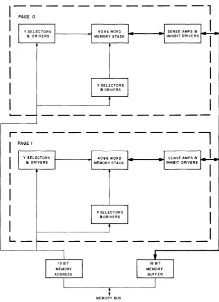
The PDP-15 Memory communicates directly with the Central Processor and the Input/Output (I/O) Processor through the memory bus. Data and instruction words of each bank are read from and written into individual memory cells through a buffered register referred to as the memory data buffer. (See the Memory Block Diagram, Figure 4-1.)
Words in a memory bank are selected according to the address in the memory address buffer. The 13-bit capacity of the memory address buffer allows 213 or 8192 words to be refer-enced in each bank.
The memory address buffer receives the memory cell address from the Central Processor or I/O Processor. The address provides the coordinates for locating a word in a memory bank.
Decoding of the memory address to select a particular word location containing 18 bits is performed by the memory selection logic. Bit 5 of the memory cell address selects which page the cell is in, and the remaining bits select the X and Y coordinates of the cell.
Bits 1 to 4 of the memory bus select lines are used to select which bank of Memory the word is in. Up to 4 banks can normally be added to the PDP-I 5 , but a special provision to expand memory up to 16 banks can be accommodated by the 18-bit address registers in the CPU.
Memory Cycles
Words are read from and written into Memory by a fixed sequence of events called a memory cycle. The memory cycle consists of a read half-cycle and a write half-cycle. Each type of half cycle requires 400 ns. Thus, the effective cycle time is 800 ns. For most applications, however, the two processors initiate a memory request and wait until the end of the read half-cycle only. At this time, the desired data is available for reading or has been accepted at the memory data buffer for writing, and the Central Processor or I/O Processor may proceed to the
next step in its logical sequence of operations and perform useful functions while the write half-cycle is taking place. Thus, main memory access operations normally cause the two proces-sors to wait only 400 ns. Delays caused by simultaneous requests by the two processors are discussed later in this section.
Read Half-Cycle - The read half-cycle copies the contents of the memory cell specified by the contents of the memory address buffer into the memory data buffer. If the parity option is present, a parity check bit is copied into the memory data buffer at the same time.
Write Half-Cycle - The write half-cycle copies the contents of the memory data buffer into the addressed memory cell. This half-cycle always occurs in conjunction with and following a read half cycle, although there may be a "pause" between them, during which the I/O Processor can manipulate the data in its Add-to-Memory mode (see I/O Data Processor Add-to-Memory Description, Chapter 5).
Parity
The parity option provides core planes that have 19 bits for each word and parity checking/ generating control logic. When the parity option is present, the accuracy of transfers to and from Memory is verified by means of parity checking. A parity bit is added to each word stored in Memory such that the total number of 1 bits in the word, including the parity bit, is odd. For example, if the 18-bit word to be stored in Memory contains an even number of Is, the parity bit is automatically made a I, and is stored with the word. When the word is later read from Memory, the computed parity bit is calculated on the basis of the content of the 18-bit word. The two parity bits are then com-pared, if they do not agree, the memory parity error alarm is turned on, causing a program interrupt or automatic priority interrupt re-quest, or simply a Halt.
All 18 bits and the accompanying parity-check bit (when present) are transferred in parallel
-PAGE 0
Y SELECTORS
a. DRIVERS
4096 WORD MEMORY STACK
X SELECTORS
a. DRIVERS
..
SENSE AMPS a. INHIBIT DRIVERSL . . - _ _ _ _ _ _ _ _ _ _ _ _
r
-I
I
I
I
I
I
L
PAGE I
Y SELECTORS
a. DRIVERS
-I
13 BIT MEMORY ADDRESS
I
4096 WORD MEMORY STACK
X SELECTORS
a. DRIVERS
;
MEMORY BUS
18 BIT MEMORY
BUFFER
[image:31.617.81.519.60.663.2]I
Figure 4-1. PDP-IS Memory Bank
SENSE AMPS 8 INHIBIT DRIVERS
I
I
I
I
I
I
I
memory data buffer, as shown in Figure 4-1. The memory data buffer is connected to the memory bus and hence to the rest of the PDP-IS System. This is also an 18-bit parallel transfer.
Memory Modularity
The PDP-IS/l 0 System contains one page of 4096 memory words. Additional modules (pages) may be added to the system. The basic system can accommodate up to 32,768 core memory words (eight 4K pages) in the basic 19-in. rack mount cabinet. Expansion beyond 32,768 words requires the addition of another cabinet to the system configuration. Memory communicates with the central processor and the I/O processor on the bidirectional, inter-locked party-line memory bus (See Figure 4-2).
1/0 BUS
110 CENTRAL
PROCESSOR PROCESSOR
MEMORY MULTIPLEXER
---MEMORY RELOCATION
I
MEMORY BUS8K
Memory Multiplexer
The memory multiplexer allows both the Cen-tral and I/O Processors to share core memory. In
the event that both request a memory cycle simultaneously, the I/O Processor will be ser-viced first and the Central Processor must wait. However, if only one processor is using Memory, then both can process at the same time. For example, the Central Processor may be execut-ing an EAE instruction while the I/O Processor transfers data out of Memory to a DECdisk.
Memory Relocation
Memory relocation is optional on all PDP-IS Systems. This feature provides a relocation regis-ter and an upper boundary regisregis-ter to permit hardware relocation of both system and user programs. It allows the relocated program to execu te only wi thin its specified boundary; thereby providing protection for all other pro-grams.
8K 8K 8K
MEMORY MEMORY MEMORY MEMORY
BANK BANK BANK BANK
0 1 2 3
IS -0003
..
...
CHAPTER 5
ORGANIZATION OF THE INPUT-OUTPUT PROCESSOR
SUMMARY OF CHARACTERISTICS
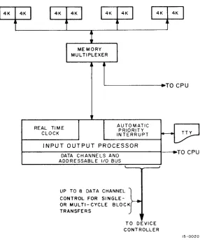
The I/O Processor contains two subunits, the data channel controller and the addressable I/O bus.
Data Channel Controller
Data Transfer Modes - Single and multicycle
block transfer, memory-increment, add-to-mem-ory
Data Channels - Eight standard Options - Real-Time Clock
Addressable I/O Bus
Features - Two cycle skip line, program
inter-rupt, teletype interface, console interface
Data Transfer Modes - Program controlled data
transfers
Device Ports - A maximum of 50 physical ports
shared between the data channels and the ad-dressable I/O bus.
Options - API - Eight levels of automatic priority
interrupts - Four hardware levels and four software levels
I/O PROCESSOR
transfers are being made between Memory and the I/O Processor, the CPU is free to operate independently. Requests from the I/O Processor for memory access are, however, given priority over CPU requests by the memory multiplexer; this can cause the CPU an occasional "cycle-stealing" delay. The structure of the I/O Proces-sor provides the following benefits to the user:
Synchronous and asynchronous devices can be handled with equal ease.
Modes of Data Transfer
Peripheral devices may transfer data in anyone of three modes: single-cycle block transfers, mul-ti-cycle block transfers, and program-controlled transfers.
The simultaneity of data transfers and CPU computing permits high-speed processing to meet the demands of real-time applications.
The I/O Processor can be expanded or re-configured at any time without major mod-ification of the rest of the system.
Data Channel Controller
User-designed or special-purpose equipment can be easily and inexpensively interfaced to the system.
The data channel controller implements the first two modes of data transfers and in addition has an add-to-memory mode and an increment mem-ory mode. The real-time clock option is also implemented in this section.
14K 4K
I
r
4K 4K1
14K 4KI
4K 4KI
MEMORY MUL TI PLEXER
REAL TIME AUTOMATIC PRIORITY
CLOCK INTERRUPT
INPUT OUTPUT PROCESSOR
DATA CHANNELS AND ADDRESSABLE I/O BUS
UP TO 8 DATA CHANNEL "" CONTROL FOR
SINGLE-~
OR MULTI-CYCLE BLOCK
TRANSFERS
,
TO DEVICE CONTROLLER
Figure 5-1. I/O Processor
TO CPU
W
- T O CPU15-0020
[image:34.612.178.464.340.684.2]•
Eight data channels are standard on all PDP-15 Systems and may serve to concurrently transfer data from eight different devices. Four of these are normally reserved for multi-cycle block transfers and the remaining four are reserved for single-cycle block transfers. However, the chan-nels are designed to accept any mixture of either single- or multi-cycle devices.
Multi-Cycle Block Transfers
Normally, four of the eight standard channels are used for multi-cycle block transfers. A two-word packet in core memory is reserved for each of these channels: locations 30 and 31 for the first, 32 and 33 for the second, 34 and 35 for the third, and 36 and 37 for the fourth. The two words in the packet are used to store the "word count" (number of words to be transferred in the block), and the "current address" (where the data is to be transferred). The I/O Processor contains the control logic and an I/O adder to automatically fetch and increment the contents of the two registers.
Data is read into memory in three I/O Processor cycles and is read out in four cycles. (The additional cycle allows I/O bus settling and the settling of control gates prior to the strobing of the data word into the device buffer register.) Three memory cycles are required for both. Maximum input rate is 250,000 words/second and maximum output rate is 181,000 words/ second, ensuring data transfer integrity.
A multi-cycle block transfer, flowcharted in Figure 5-2, is initiated by an input/output in-struction after the two core registers have been initiated by minus the word count and the current address minus one. During the first cycle, the contents of the word-count register are incremented by one and restored. During the second cycle, the current address is incremented by one and restored, in addition to being trans-ferred to the memory address buffer of memory. During the third cycle (or fourth in the case of output), the actual data transfer occurs. The I/O Processor continues to transfer data sequentially until the word-count register reaches zero, at which time an interrupt is generated to notify
the monitor that the block transfer is complete. Because these multi-cycle block transfers are completely automatic in nature and do not require any CPU attention except for the I/O transfer initialization, the CPU is free to com-pute while they are taking place. The only limi tation on simultaneity lies in the sharing of memory. The I/O Processor has first priority on memory requests and effectively "locks out" the CPU for three cycles. As data transfer rates approach maximum, the CPU can be completely locked out.
Figure 5-3 illustrates how the data channel controller registers implement the multi-cycle transfers .
Assume the two-word core-memory packets assigned to a given multi-cycle data channel have been loaded by the respective I/O service rou-tine. For the case of data input to memory the following occurs:
An instruction from the service routine enables the device controller. This allows the controller to request a data transfer from the I/O processor.
When the device controller's data buffer registers are full it issues a "data channel request."
The I/O Processor, if not busy, acknow-ledges the request by returning a "data channel grant."
The device controller then generates a fixed code pointing to its packet address in core memory. This is transmitted over the com-mon I/O bus address lines and is stored into the data storage register of the data channel controller through the I/O adder. The adder is inhibited during this operation.
The I/O Processor then generates a "mem-ory cycle request."
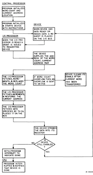
CENTRAL PROCESSOR PROGRAM INITIALIZES WORD COUNT AND CURRENT ADDRESS LOCATION
l
PROGRAM INITIALIZES DEVICE
a STARTS DEVICE
-WITH INSTRUCTIONS WHEN DEVICE HAS
I
DATA READY OR NEEDS DATA A RE-110 PROCESSOR QUEST IS PLACED WHEN THE I/O PRO- ON THE I/O BUS CESSOR IS READY AI
GRANT IS ISSUEDTO REQUESTING DEVICE
I
THE DEVICESUPPLIES THE ADD-RESS OF THE WORD
•
COUNT,CURRENT ADDRESS PAIR
I
l
DEVICE CLEARS ITSTHE 110 PROCESSOR IF WORD COUNT ENABLE AFTER FETCHES ,INCRE- OVERFLOW, THEN AN CURRENT WORD MENTS, a REPLACES OVERFLOW IS SENT HAS BEEN THE WORD COUNT TO DEVICE TRANSFERRED
l
THE I/O PROCESSOR FETCHES,INCREMENTS,
a RESTORES THE CURRENT ADDRESS
~
THE I/O PROCESSOR FETCHES DATA SPECIFIED BY TH CA, PLACES IT ON THE BUS
I
~
j:HEI DEVICE STROBES THE DATA INTO ITS REGISTER
IS NO DEVICE
•
STILL ENABLED ?SET A, PROGRAM YES
INTERRUPT TO INDICATE DONE CPU
•
PROGRAM I NTER-RUPTED a NOTIFIED THAT DEVICE IS DONE
15 -0004
[image:36.613.150.472.68.673.2]TO MEMORY BANKS
1
j
I
r--- ---
- - - ---
- - - ,+
I
I
I
I I I I I I
I
I
DATA STORAGE REGISTER
110 ADDER MIXER LOGIC
r
BUS BUFFER
MEMORY GRANT
MEMORY REQUEST
REQUESTI GRANT
LOGIC
110
PROCESSOR
I I
I
I
I
CENTRAL PROCESSOR
L _______________________________ ~~S.:!S2~.J
IIOOFLO FROM TOIFROM BIDIRECTIONAL
//0 BUS I/O BUS DATA II NES ADDRESS
LI NES
DATA CHANNEL
GRANT TO
1/0 BUS
DATA CHANNEL REQUEST
IS-0005
Figure 5-3_ Multi-Cycle Transfer Implementation
The address data in the data storage register is then stored into the memory address (MA) register of the memory bank I and the data (word count) from the first word of the packet that the MA is now pointing to, is transmitted out of memory and into the data channel controller's adder. The word count data word is incremented by one and stored back into memory_ If dur-ing this incrementdur-ing the adder overflows (indicating that the current address was the last), then an I/O overflow pulse is trans-mitted back to the device to disable future
data-channel requests and also to post an interrupt to the Monitor.
This "word count" operation occurs in one I/O processor cycle, using one memory cycle_
[image:37.615.86.520.65.480.2]packet - the "current address," which is then transmitted back to the adder, incre-mented by one and strobed back to mem-ory. During the third I/O processor cycle, the current address is strobed into the MA register to point to the data array word where the I/O data will be transferred. The data is then gated from the device con-troller, through the adder, (which is inhib-ited during this cycle), and into memory.
A memory request/grant synchronization again occurs; and
The data in the storage register is strobed into the data array ending the cycle.
Data output follows the same sequence, with the exception that one additional I/O processor cycle is required to allow the bus to settle before data is strobed out of memory and into the device.
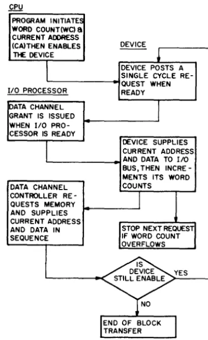
Single-Cycle Block Transfers
Single-cycle block transfers, flowcharted in Figure 5-4, are used by high-speed peripherals that normally transfer complete records (blocks) of information, such as disks and CRT devices. A single cycle of the I/O Processor takes I JJ.S
allowing a maximum transfer rate of up to one million 18-bit words per second.
High-speed hardware registers, designed into the device controllers of the high-speed peripherals, store the "current address" (the memory cell where data is currently being transferred), and the "word count" (the number of words remain-ing to be transferred in a block). These registers are loaded by input/output transfer (lOT) in-structions issued by the CPU. Device testing and initialization are handled by the CPU via lOTs to provide supervisory control. A subsequent lOT initiates the data transfer. The I/O Processor uses the current address information to address core memory, then strobes the data between memory and the device controller buffer regis-ter. Logic within the device controller then
increments the current address register and the word count register to provide sequential block transfer. .
CPU
-PROGRAM INITIATES WORD COUNT(WC) a CURRENT ADDRESS
(CAl THEN ENABLES DEVICE
-~
TI£ DEVICE
DEVICE POSTS A SINGLE CYCLE RE-QUEST WHEN
1/0 PROCESSOR READY DATA CHANNEL
J
GRANT IS ISSUED WHEN 110
PRO-cEssoR IS READY
DEVICE SUPPLIES CURRENT ADDRESS AND DATA TO 110 BUS, THEN INeRE-MENTS ITS WORD DATA CHANNEL COUNTS
CONTROLLER
RE-I
QUESTS MEMORY AND SUPPLIES CURRENT ADDRESS
AND DATA IN STOP NEXT REQUEST SEQUENCE IF WORD COUNT
OVERFLOWS IS
DEVICE YES
?
NO lEND OF BLOCKTRANSFER
[image:38.620.343.548.117.451.2]15-0006
Figure 5-4. Single Cycle Block Transfer, Flowchart
When the word count register overflows at the end of a block transfer, an interrupt is generated to allow the monitor system to take further action. Typically, this action will include discon-necting the device from the I/O bus or reloading the device controller registers for another block transfer. The maximum number of words that may be transferred in a single-block is 32,768.
controller, and has then enabled it, the following occurs:
The device controller posts a single-cycle data channel request to the I/O Processor.
The I/O Processor, as soon as it becomes available, acknowledges the request by re-turning a "Data Channel Grant."
The device then strobes both its current address and its data onto the I/O bus to the I/O Processor.
The data channel controller feeds the cur-rent address through its adder (which is inhibited throughout the single cycles) to the data storage register. A memory cycle is requested, and this address is strobed into a memory bank's address buffer. The data is then strobed off the 18 I/O data lines and into the memory location specified by the current address.
During this operation, the device incre-ments its own word count, and disables itself on overflow. It then posts an inter-rupt to the monitor to indicate that its operation has been completed.
Increment Memory
The increment memory mode allows an external device to add one to the contents of any memory location in a single cycle; this feature is most commonly employed in the accumulation of data in histogram form. Effectively, the incre-ment memory mode simply goes through the word-count cycle of a multi-cycle channel trans-fer, and then stops. The maximum rate at which it can increment is 500 kHz. This feature is particularly useful for in-core scaling and count-ing in pulse height analysis.
Add-To-Memory
Add-to-memory is a standard feature of the PDP-IS that adds unique capabilities to the already powerful I/O facilities.
In add-to-memory mode, the contents of an external register can be added to the contents of a memory location in four cycles. This feature is extremely valuable in signal averaging and other processes requiring successive sweeps for signal enhancement.
The add-to-memory operation is a combination of cycle data channel input and multi-cycle data channel output operations. The data transmitted by the device is added to a word read out of memory as specified by the current address, and the result is rewritten into the same location. It is simultaneously transmitted to the device via the I/O bus. Four I/O processor cycles are required.
Real-Time Clock
When enabled, the real-time clock counts, in memory location 00007, the number of cycles completed by anyone of three inputs:
a. The line voltage (50 or 60 Hz)
b. Any standard DEC clock may be op-tionally installed.
c. A user supplied TTL compatible signal which can be fed through a coaxial cable to a BNC connector on the PDP-IS.
When location 00007 overflows, an internal program interrupt (or API request, if available) is generated informing the monitor that its preset interval is over. The monitor must either disable the clock or reinitialize location 00007 to the 2's complement of the number of counts it needs to tally.
The incrementing of location 00007 during a real-time clock request occurs via the I/O proces-sors' increment memory facility. A real-time clock request takes priority over API, Pl and lOT requests, but not over block transfers.
ADDRESSABLE I/O BUS
program interrupt and the automatic priority interrupt (API) option.
Program-Controlled Transfer
Program-controlled transfers, implemented by input/output transfer (lOT) instructions, can move up to 18 bits of data between a selected device and the accumulator (AC) in the CPU. The devices involved are connected to the ad-dressable I/O bus portion of the I/O processor. A total of up to 50 device controllers may be attached to this bus and to the data channels. lOT instructions are microcoded to effect re-sponse only for a particular device. The micro-coding includes the issuing of both a unique device selection code and the appropriate pro-cessor-generated input/output pulses to initiate a specific operation. For an "out" transfer, the program reads a data word from memory into the AC. A subsequent lOT instruction places the data on the bus, selects the device, and transfers the data to the device. For an "in" transfer, the process is reversed; an lOT instruction selects the device and transfers data into the AC. A subsequent instruction in the program transfers the word from the AC to memory. Maximum transfer rate in this mode is 100,000 words per second.
As previously mentioned, lOT instructions are also used to initialize the single- and multi-cycle channels and the transfer word count and cur-rent address information to the single-cycle de-vice controllers. In addition, these instructions are used to test or clear device flags, select modes of device operation, and control a num-ber of processor operations.
A PDP-IS lOT instruction, Figure 5-5, contains the following information:
a. An operation code of 70s .
b. An 8-bit device selection code to dis-criminate between up to 128 user periph-eral devices (selection logic in a device's I/O bus interface responds only to its pre-assigned code). In normal practice, bits 6 through I I perform the primary device
discrimination between up to 42 devices, with bits 12 and 13 coded to select an operational mode or subdevice.
c. A command code (bits 14 through 17) capable of being microprogrammed to clear the AC and issue up to three pulses via the I/O bus.
Operation Device Clear AC at Generate an lOP Code 70 Selection Event Time 1 2 Pulse at Event
I
I ~,,..o----l~---,51(
,..6--~-'
11 \ .I
2:-1 17I : : : :
::::: ::::::1
Sub-Device Selection
,L,-t
IJ
Generate an Generate an lOP 4 Pulse lOP 1 Pulse at at Event
Time 3
Event Time 1
Figure 5-5. lOT Instruction Format
are normally used to effect programmed trans-fers of information from the AC to a selected device. These conventions do not, however, pre-clude use of the lOP pulses to effect other external functions if the following restrictions are observed.
The usual uses of lOPs are:
lOP 1 -Normally used in an I/O skip instruction to test a device flag. May be used as a command
FETCH EVENT TIME 1
pulse, but may not be used to initiate either a "load of" or a "read from" a device.
lOP2 -Usually used to transfer data to or from the device to the computer, or to clear device's information register. May not be used to deter-mine a "skip" condition.
lOP4 - Used only to transfer data from the computer to the device. May not be used to determine a "skip" condition or to transfer data to or from the computer.
NEXT EVENT TIME 2 EVENT TIME 3 FETCH _ 0.75_
,- J.l.SEC -,
-, *
r-~---~---~, I I I
: I I
I ' IOP1 I 100 n SEC
:-.r
-I-- IWORSE CASE I I
t-
J's1~-1I : -;
*
r---i
I I ,
I I '
I I ' (OP2
I 100 n SEC~---I-- 0.50
I ·NORSE CASE I -IJ.l.SEC
I--I I
,--,*
,...-~I ' I
I I 100 n SEC~ ___
I I WORSE CASE , I
I I I , IIOP4
I I I L __
r--
1.0J.l.SEC+ 1.0J.l.SEC-+-
1.0J.l.SEC+1.O~SEC----l
[image:41.617.166.484.220.463.2]*
NOMINAL PULSE WIDTHFigure 5-6. Machine Cycles for lOT Instruction Execution
PROGRAM INTERRUPT FACILITY
The program interrupt (PI) system, standard on all PDP-IS Systems, provides for servicing a peripheral device at rates up to 50 kHz.
The program interrupt (PI) facility, when en-abled, relieves the main program of the need for repeated flag checks by allowing the ready status