warwick.ac.uk/lib-publications
A Thesis Submitted for the Degree of PhD at the University of Warwick
Permanent WRAP URL:
http://wrap.warwick.ac.uk/94010
Copyright and reuse:
This thesis is made available online and is protected by original copyright.
Please scroll down to view the document itself.
Please refer to the repository record for this item for information to help you to cite it.
Our policy information is available from the repository home page.
Tunnelling effects in multiferroic tunnel junctions
by
Geanina Apachitei
Thesis
Submitted to the University of Warwick
for the degree of
Doctor of Philosophy
Physics
Contents
List of Figures iv
List of Tables xiii
Acknowledgments xiv
Declarations xv
Abstract xvii
Abbreviations xviii
Chapter 1 Introduction 1
Chapter 2 Theoretical background 4
2.1 Quantum tunnelling . . . 4
2.2 Transport mechanisms in thin film structures . . . 8
2.2.1 Direct tunnelling . . . 9
2.2.2 Thermionic injection . . . 11
2.2.3 Fowler-Nordheim tunnelling . . . 11
2.3 Magnetic tunnel junctions . . . 11
2.3.1 Ferromagnetic materials . . . 12
2.3.2 Magnetoresistance effects . . . 15
2.3.3 Tunnelling magnetoresistance . . . 15
2.4 Ferroelectric tunnel junctions . . . 17
2.4.1 Ferroelectric materials . . . 17
2.4.2 Tunnelling electro-resistance . . . 18
2.5 Multiferroic tunnel junctions . . . 20
2.6 Materials used in multiferroic tunnel junction fabrication . . . 20
2.6.2 Lanthanum strontium manganate (La0.7Sr0.3MnO3) bottom
electrode . . . 22
2.6.3 Ferroelectric lead zirconium titanate PbZr0.2Ti0.8O3 . . . 23
2.6.4 Ferroelectric lead titanate (PbTiO3) . . . 23
2.6.5 Antiferroelectric lead zirconate (PbZrO3) . . . 24
2.6.6 Cobalt top electrode . . . 25
2.7 Summary . . . 25
Chapter 3 Experimental methods 27 3.1 Thin film growth . . . 27
3.1.1 Pulsed Laser Deposition (PLD) . . . 27
3.1.2 Reflection High Energy Electron Diffraction (RHEED) . . . . 29
3.1.3 Co top electrode sputtering . . . 31
3.2 Surface characterisation . . . 32
3.2.1 Atomic Force Microscopy (AFM) . . . 32
3.3 Structural characterisation . . . 34
3.3.1 X-Ray Diffraction (XRD) . . . 35
3.3.2 Transmission Electron Microscopy (TEM) . . . 36
3.4 Magnetic and electric characterisation . . . 38
3.4.1 Vibrating Sample Magnetometer (VSM) and Superconducting Quantum Interference Device (SQUID) . . . 38
3.4.2 Physical Properties Measuring System (PPMS) . . . 39
3.4.3 Cryoprober . . . 40
3.4.4 Ferroelectricity testing . . . 40
3.5 Summary . . . 41
Chapter 4 Fabrication and characterisation of multiferroic tunnel junctions 42 4.1 SrTiO3 substrate treatment . . . 42
4.2 Growth and characterisation of (La,Sr)MnO3 bottom electrode . . . 44
4.3 Growth and characterisation of PbTiO3 barrier . . . 49
4.4 Growth and characterisation of PbZrO3 barrier . . . 52
4.5 Co top electrode . . . 54
4.6 Summary . . . 55
Chapter 5 Size effect in LSMO/PTO/Co ferroelectric tunnel
junc-tions 56
5.1.1 Formation of local polarisation vortices in LSMO/PTO/Co
tunnel junctions . . . 57
5.1.2 Critical thickness for ferroelectricity in STO/LSMO/PTO sys-tem . . . 65
5.2 Transport mechanisms in LSMO/PTO/Co tunnel junctions . . . 68
5.2.1 Analysis of the I(V) curves . . . 69
5.2.2 Temperature dependent tunnelling mechanisms . . . 73
5.3 Tunnelling magnetoresistance . . . 75
5.3.1 Low temperature tunnelling magnetoresistance . . . 75
5.3.2 TMR variation with temperature . . . 79
5.4 Influence of polarization orientation on tunnelling junction transport 81 5.4.1 Thickness and temperature dependence of electronic transport 83 5.4.2 Size effect of magnetoelectric coupling . . . 91
5.4.3 Tunnelling magnetoresistance dependence on applied bias . . 93
5.4.4 Temperature-dependent magnetoelectric coupling . . . 96
5.5 Summary . . . 98
Chapter 6 Multiferroic tunnel junctions with PZO barrier 99 6.1 Antiferroelectric tunnel junctions at room temperature . . . 100
6.2 Temperature dependent electric measurements . . . 106
6.3 Influence of ferroelectric polarisation on spin transport . . . 109
6.3.1 Voltage-dependence of tunnelling magnetoresistance . . . 111
6.3.2 Tunnelling magnetoresistance in devices with 6.5 nm thick PZO barrier . . . 113
6.4 Summary . . . 117
Chapter 7 Conclusions 118 7.1 Summary . . . 118
7.2 Outlook . . . 119
List of Figures
2.1 a) Tunnelling process highlighting the wave function exponential de-cay through the barrier and transmission into the second electrode; b) asymmetric square barrier profile with the wave function compo-nents for the two metals; c) metal/insulator/metal tunnelling device schematics. . . 5 2.2 a) Tunnelling junctions barrier profile under applied bias; b) direct
tunnelling; c) thermionic emission; d) Fowler- Nordheim tunelling mechanisms; reproduced from [20]. . . 9 2.3 Difference between the density of states (DOS) of a) non-magnetic
metals and b) ferromagnets. . . 12 2.4 Schematic drawing of relative spin orientations in: a) ferromagnetic;
and b) antiferromagnetic materials. . . 13 2.5 Normalised magnetisation hysteresis loops for magnetic field varied
along the easy axis (red) and hard axis (black) of a ferromagnetic sample. . . 13 2.6 Cross sectional view of the domain wall structure: a) Bloch domain
wall in thick films; b) Neel domain wall in thin films; reproduced from [28]. . . 14 2.7 Intuitive image of exchange bias at the ferromagnet/antiferromagnet
interface illustrated on a hysteresis loop after field cooling from a temperature higher than the Neel temperature of the antiferromagnet and lower than the Curie temperature of the ferromagnet; reproduced from [30]. . . 14 2.8 a) Resistance change of a magnetic tunnel junction correlated with
2.9 a) FerroelectricP(V) hysteresis (top) with corresponding resistance changes at the coercive voltage values (bottom); b) Schematics of changes in the barrier potential caused by polarisation switching which reflect on the resistance values in the two states; c) mecha-nisms leading to TER effect; adapted from [39]. . . 19 2.10 a) Tunnelling mechanisms contribution to the electroresistance (ER)
with variation of applied voltage and barrier thickness, higlighting the transition regions; b) slice from the plot in a) representing the thickness dependence of ER at high (red dashed-dotted line) and low voltages (solid blue and green dashed lines); reproduced from [41]. . 20 2.11 a) Schematics of the fabricated multiferroic tunnel junctions; b)
schemat-ics of in-plane lattice parameters of the STO substrate, pseudocubic LSMO electrode and the PTO, PZT and pseodocubic PZO barriers. 21 2.12 Representation of: a) STO, b) PTO unit cells [42] realised with
Crys-talMaker software using National Chemical Database Service [43]. . 21 2.13 a) Schematic representation of crystal field splitting in 3dband energy
levels: isolated manganese ion (left), an octahedral crystal field (mid-dle) and a Jahn Teller distortion in the form of a tetrragonal crystal field (right) with the coresponding electron localisation surfaces of the orbitals; b) majority and minority spin bands characteristic to half-metals illustrated in La2/3Sr1/3MnO3; adapted from [50, 51, 52]. 22
2.14 PZT phase diagram highlighting the structure and Curie temper-ature dependence on the composition, where AO: antiferroelectric
orthorhombic; PC: paraelectric cubic; FRHT: ferroelectric
rhombo-hedral at high temperature; FRLT: ferroelectric rhombohedral at low
temperature; FT: ferroelectric tetragonal, MPB: morphotropic phase boundary and MPC: morphotropic phase composition; reproduced from [62, 63] . . . 24 2.15 a) PZO orthorhombic unit cell; b) projection highlighting the
dis-placements of Pb ions and the pseudocubic unit cell and c) pseu-docubic unit cell of PZO; adapted from [71]. . . 25
3.2 Representation of the deposition and growth illustrating differences in growth modes: a) layer-by-layer (Frank-van der Merwe); b) layer + island (Stranski- Krastanov) and c) island (Volmer-Weber). . . 29 3.3 a) Diffraction conditions shown in reciprocal space by the
intersec-tion of the Ewald sphere of the electron beam with selected sample reciprocal lattice rods creating the 0th order Laue circle; b) top view and c) side view of the Ewald sphere and reciprocal lattice rods of the sample. . . 30 3.4 a) RHEED specular spot intensity showing oscillations corresponding
to La0.7Sr0.3MnO3layer-by layer growth; the moments where the laser
started and stopped ablating are marked; b) Determination of the deposition rate from the number of deposited unit cells variation with the number of ablation pulses. . . 30 3.5 Steps in the patterning process of the Co top electrode:
photolitog-raphy and wet etching. . . 32 3.6 Atomic force microscopy principle- reproduced from [81]. . . 33 3.7 PFM detection of the deformation resulting from the inverse
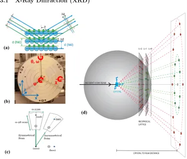
piezo-electric effect- reproduced from [86]. . . 34 3.8 a) Diffraction (reflection) process on parallel atomic planes; b)
pos-sible rotations of sample position in XRD; c) RSM scans principle and d) RSM measurement principle involving the Ewald sphere and reciprocal lattice of the sample. . . 35 3.9 Electron ray path in TEM in: a) diffraction; b) bright field and c) dark
field modes, depending on the diaframg and lens settings; reproduced from [89]. . . 37 3.10 a) Transient current in a ferroelectric capacitor and triangular voltage
applied during ferroelectricity testing; b) switching current-voltage (red) and polarisation-voltage (green) hysteresis loops measured in a LSMO/PZT/Cu capacitor, illustrating the coercive field and remnant polarisation values. . . 40
4.2 a) RHEED oscillations of the specular spot intensity showing the number of LSMO layers deposited; insert: RHEED diffraction pattern after LSMO deposition; b) AFM image of the surface; c) (002) plane diffractogram of STO and LSMO and d) RMS around the (103) plane of STO. . . 45 4.3 a) TEM image of final LSMO(60 u.c.)/PTO(6 u.c.)/Co tunnel
junc-tion illustrating the quality of LSMO film in report with the STO substrate and the PTO film; b) high resolution scanning TEM image showing the in-plane and out-of-plane intensity profile in LSMO: the highest peaks correspond to La/Sr atom columns, the less visible ones out-of-plane correspond to the O/Mn columns. . . 46 4.4 a) Hysteresis loop of LSMO magnetic moment measured at 10 K; b)
magnetic moment vs. temperature and its derivative indicating the Curie temperature TC; c) LSMO resistivity variation on temperature
and its derivative showing TC = 360 K; d) hysteresis loops measured
in-plane (easy axis) and out-of-plane at 300 K; LSMO resistance mea-sured e) in-plane and f) out-of-plane at 300 K. . . 48 4.5 a) RHEED oscillations showing layer-by-layer PTO growth; insert:
diffraction pattern after the deposition; b) deposition rate determined from RHEED for 12 u.c. PTO film; c) AFM image of the PTO surface. 50 4.6 a) 2θ−ω scan of the (002) peaks of STO, LSMO and PTO; b) RSM
around STO (103) peak; annular dark field, c) and e) and bright field TEM images, d) and f) of 3 u.c. (top) and 12 u.c. (bottom) PTO tunnel junctions. . . 51 4.7 a) RHEED diffraction pattern showing the additional spot caused by
the PZO film growth; b) AFM image of the PZO surface; c) TEM dark field image of the local structure and d) increased magnification of the area marked in c). . . 52 4.8 RSM of STO/LSMO/PZO for a) 85 nm and b) 12.5 nm thick PZO;
c-d) P(V) hysteresis loops for the same thicknesses. . . 53 4.9 a) Magnetic moment variation with temperature and its first
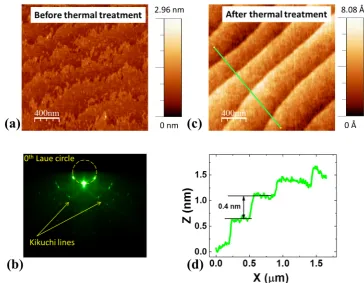
5.1 a) Schematic oxygen displacement in the projection of the (110) plane of a perovskite; b) oxygen displacement measured from an experimen-tal image of LSMO; reproduced from [3]. . . 58 5.2 a) Atomic resolution ADF image; b) atom column intensity showing
the different compositions of the films; c) ABF signal collected simul-taneously with a); d) magnified regions to show the LSMO and PTO structure with different contrast; e) quiver plots showing dipoles mea-sured from c); f-g) enlarged vortices from the regions marked in e); h) average out-of-plane polarisation across the domains; error bars are represented by standard error of the mean; reproduced from [3]. . . . 60 5.3 Average of polarisation across the thickness of a 9 u.c. PTO film
with highlight on the LSMO/PTO interface: values are obtained from averaging rows of unit cells and the error bars are the corresponding standard errors of the means; reproduced from [3]. . . 61 5.4 Atomic resolution images in: a) ADF and b) ABF modes of a 6 u.c.
PTO film; c) corresponding plot quiver plot of the dipoles; d) large area analysis including a dipole map, ABF and ADF images with insets of the regions of interest in e-g); reproduced from [3]. . . 62 5.5 a) ADF and b) ABF atomic resolution images; c) corresponding
quiver plot of the local dipoles in a 3 u.c. thick PTO film; repro-duced from [3]. . . 64 5.6 Local hysteresis loops for 6 u.c., a) and b) and 3 u.c., c) and d) PTO
films; the amplitude and phase were measured by PFM with electric field applied on the conducting tip, a) and c) and in a remnant state after the field was removed, b) and d). . . 65 5.7 a) 5×5 µm2 scan of 6 u.c. PTO film: a) PFM amplitude signal and
b) PFM phase signal; c-d) line profile corresponding to the blue lines in the amplitude and phase scans. . . 66 5.8 Hysteresis obtained by applying voltage pulses for LSMO/PTO/Co
samples with a) 12 u.c.; b) 9 u.c. and c) 6 u.c. PTO barriers; d) sequence of writing and reading voltages; e) polarisation orientation in the ON and OFF states. . . 67 5.9 a) Current-voltage characteristics in the P↑ and P↓ states for 6, 9
5.10 Parabolic dependence of the conductance in the two states for: a) 6 u.c., b) 9 u.c. and c) 12 u.c. thick PTO devices, where G0=7.748×10⁻⁵
S is the quantum conductance. . . 70 5.11 Logarithmic representation showing the transition from direct
tun-nelling to Fowler-Nordheim tuntun-nelling for devices with 6, 9 and 12 u.c. thick PTO and schematic representation of the corresponding barriers and tunnelling process from the LSMO to the Co electrode; the black points represent the transition voltage from DT to FNT mechanisms. . . 71 5.12 a-c) Direct tunnelling fit of the current-voltage characteristics with
Brinkman model; d-f) schematics of the barrier profiles indicating the barrier parameters obtained from the fit (Table 5.1) for tunnel junctions containing 12, 9 and 6 u.c. PTO. . . 72 5.13 a) Logarithmic dependence of current density (J) on voltage at
dif-ferent temperatures; b) two-dimensional color map of J with applied voltage and temperature from a); c) logarithmic representation of I/V2 as a function ofd/V highlighting direct tunnelling and Fowler-Nordheim tunnelling processes in a tunnelling junction having 9 u.c. PTO and d) magnified plot of c) where the black points represent the DT-FNT transition voltage. . . 74 5.14 Logarithmic plot of the conductivity for devices with 6, 9 and 12 u.c.
PTO with linear fit at low and high temperatures (green lines). . . . 75 5.15 Magnetic hysteresis (blue-top) and TMR (green-bottom)
measure-ments for structures with: a) 12; b) 9; c) 6 and d) 3 u.c. thick PTO; in the schematics in a) the arrows illustrate the magnetisation alignment of the electrodes. . . 76 5.16 a) TMR effect in tunnel junctions with 3, 6, 9 and 12 u.c. PTO;
b) reduced TMR values extracted from a) compared to the reduced magnetization of LSMO; c) TMR as a function of temperature for devices with 6 u.c. PTO barrier. . . 80 5.17 a) Resistance of 3 u.c. thick PTO barrier containing pinholes
mea-sured with the variation of temperature and b) magnetoresistance loops measured at different temperatures. . . 82 5.18 TMR measured in P↑(black plots) and P↓(red plots) states showing
5.19 Temperature dependence of the junction resistance and calculated TER (left) and current-voltage dependences at 10 K (right) measured on tunnel junctions with a-b) 12 u.c.; c-d) 9 u.c.; e-f) 6 u.c. and g-h) 3 u.c. thick PTO barriers. . . 86 5.20 Resistance measured in: a) P↓ and b) P↑states without field and in
the parallel magnetisation state at -5kOe field. . . 87 5.21 Tunnelling current dependence on temperature measured at 5 mV fit
with the Glazman-Matveev (GM) model (left) in a) 6, b) 9 and b) 12 u.c. thick PTO devices in the P↓ state; d-f) (right) detailed view indicating the number of channels resulting from the fit. . . 89 5.22 TMR loops for a) 3 u.c. (as grown state), b) 6 u.c., c) 9 u.c. and d) 12
u.c. thick PTO in the P↑and P↓states; e-f) one of the possible mech-anisms to cause polarisation dependent TMR: different magnitudes of the induced magnetic moment on Ti by Co in the two states. . . . 90 5.23 a) TMR magnitude in P↑ (black) and P↓ (red) states depending on
barrier thickness at 10 K (left) and calculated TEMR (right-green); voltage-dependence of TMR for: b) 3 u.c., c) 6 u.c. and d) 12 u.c. thick PTO. . . 94 5.24 a) Intermediary resistance states after partial polarisation switching
with increasing voltage amplitude pulses in devices with 6 u.c. PTO barrier; b) variation of TMR between P↑and P↓; c) TMR as a func-tion of f-the fracfunc-tion of domains having polarisafunc-tion towards LSMO electrode, fitted with a linear function (blue line); d) schematics of the contribution of domains to the junction resistance during switching, as resistances connected in parallel. . . 95 5.25 a) TMR curves measured in the P↑ (black) and P↓ (red) states with
increasing temperature for tunnel junctions with 9 monolayers of PTO; b) variation of the resistive states (orientation of magnetisation and polarisation shown schematically) corresponding to the TMR in a) and c) TMR in P↑ and P↓ states of 9 u.c PTO (filled symbols) compared to 6 u.c. PTO (empty symbols); inset: TEMR variations with temperature for the two samples. . . 97
6.2 a-b) Barrier profiles for the 11 u.c. and 16 u.c. PZO devices corre-sponding to c-d);I(V) characteristics for c) 11 u.c., d) 16 u.c. and e) 22 u.c.; f) 27 u.c. thick PZO barriers. . . 102 6.3 a-b) Fitting with the Fowler-Nordheim tunnelling mechanism on the
2nd and 4th I(V) dependences; c) experimental data with direct tun-nelling model (red line) and FNT model (blue lines) dependencies. . 104 6.4 Variation of coercive AFE-FE (forward) and FE-AFE (backward) a)
voltage and b) field with PZO thickness for positive and negative values of the voltage. . . 105 6.5 a-b) Magnetic moment dependence on the external magnetic field
correlated with; c-d) tunnelling magnetoresistance effect for 11 and 16 u.c. PZO junctions, respectively; the schematic arrows indicate the parallel and antiparallel orientations of the LSMO and Co mag-netisations when sweeping the magnetic field. . . 107 6.6 Temperature-dependence of minimum (ON state-black plot) and
max-imum (OFF state- red plot) resistance values measured at 100 mV and the resulting TER (blue plot) for a tunnel junction with a 6.5 nm thick PZO barrier; inset: zoom on the resistance in the OFF state.108 6.7 Conductance of a tunnel junction containing 6.5 nm PZO in the OFF
state, measured with temperature at 5 mV and fitted with Glazman-Matveev model (green line). . . 108 6.8 a) The two reversible resistive states (ON-black plot and OFF- red
plot) of tunnel junctions with 6.5 nm PZO atT=10 K; b) the corre-sponding current-voltage curves fitted with a direct tunnelling model; c) resistance dependence on applied magnetic field in the two states. 110 6.9 a) TMR as a function of the applied voltage in P↑ (black) and P↓
(red) states measured at 10 K for a tunnel junction with 6.5 nm thick PZO barrier; b-c) TMR measured at -0.1V; d-e) TMR measured at 0.1 V highlighting the change from normal to inverse with polarisation reversal. . . 112 6.10 a-b) Schematics of Zr and O ions position relative to Co in P↑and P↓
6.11 a) Normal TMR loops measured at different temperatures in junc-tions containing 6.5 nm PZO barrier and b) temperature-variation of the resistance in parallel and antiparallel alignment and TMR values. 115 6.12 a) TMR loops at different temperatures of a conducting PZO
List of Tables
5.1 Estimation of the barrier parameters from fitting with Brinkman model for direct tunnelling . . . 73 5.2 TMR sign in tunnel junctions containing LSMO and Co electrodes
and Ti-based barriers . . . 78 5.3 Estimations of the parameters from fitting with the Glazman-Matveev
model . . . 91 5.4 Experimentally determined magnetic moment coupling of Ti ions
Acknowledgments
I would like to thank Prof. Marin Alexe, my supervisor for introducing me to the
subject of thin film growth and microelectronics and for giving me the opportunity
to do a PhD in this exciting field. I would also like to thank him for his
encourage-ment, support and advice on physics, as well as life in general. I would like to thank
every member of the Department of Physics who have helped me get to this point.
I am grateful to Prof. Dietrich Hesse for allowing me to use the PLD system in the
’Max Planck’ Institute for Microstructure Physics in Halle and everyone there for
all their help.
I am extremely grateful to Dr. Andy Quindeau for introducing me to the practical
aspects of tunnelling devices and training me in thin film growth, as well as for
thoroughly reading the first chapter.
I would like to thank Jon Peters for training me in TEM sample preparation and
image acquisition, as well as Dr. Ana Sanchez and Dr. Richard Beanland in the
Warwick Microscopy Group for their guidance in TEM and fruitful collaboration. I
also appreciate the time and effort put into training and discussions by Dr.
Mar-tin Lees (magnetic measurements), Dr. David Walker (X-ray diffraction) and Dr.
Dongjik Kim (PFM).
I would like to express my deep gratitude to the Electronic Functional Materials and
Surface and Interface Groups at Warwick University, the group from ’Max Planck’
Institute and the Dielectrics, Ferroelectrics and Multiferroics Group at ’Al. I. Cuza’
University in Iasi, Romania for all the helpful conversations and encouragements.
I would like to acknowledge Daniel Brunt for helping me with Latex and offering
Declarations
I declare the content of thesis is my own work except where states otherwise. The
growth was carried out at the ’Max Planck’ Institute for Microstructure Physics in
Halle Germany, as well as part of structural and electrical characterisation. The
main part of characterisation and investigations were performed in the Department
of Physics at the University of Warwick, during the period of October 2013 to March
2017 under the supervision of Prof. Marin Alexe. The research carried out here has
not been submitted, either fully or in part, for admission to a higher degree in any
other academic institution. The transmission microscopy sample preparation and
analysis in Chapter 5 has been done by Jonathan James Prescott Peters under the
supervision of Dr. Ana Sanchez in the Warwick Microscopy group. The
piezore-sponse force microscopy experiment in the same chapter was realised with the help
Work carried out by the author of this thesis during the PhD published in
refereed journals:
• Antiferroelectric tunnel junctions, Geanina Apachitei, Jonathan J. P. Peters,
Ana M. Sanchez, D.J. Kim, Marin Alexe, Advanced Electronic Materials
(2017)
• Polarization curling and flux closures in multiferroic tunnel junctions, Jonathan
J. P. Peters,Geanina Apachitei, Richard Beanland, Marin Alexe and Ana M.
Sanchez, Nature Communications 7 (2016): 13484.
• Four-state ferroelectric spin-valve, Andy Quindeau, Ignasi Fina, Xavi Marti,
Geanina Apachitei, Pilar Ferrer, Chris Nicklin, Eckhard Pippel, Dietrich Hesse
and Marin Alexe, Scientific Reports 5 (2015).
Work presented in this thesis and at the moment waiting to be submitted to
a refereed journal:
• Polarisation influence on spin transport in multiferroic tunnel junctions with
PbTiO3and PbZrO3barriers,Geanina Apachitei, Marin Alexe, in preparation
Work in this thesis presented at international conferences by the author:
• Polarisation effect on tunnelling magnetoresistance in multiferroic tunnel
junc-tions, Geanina Apachitei, Marin Alexe, TO-BE Spring Meeting, 3-5th April
2017, Luxembourg, Luxembourg (poster)
• Ferroelectric and antiferroelectric tunnel junctions,Geanina Apachitei, Marin
Alexe, TO-BE Spring Meeting, 6-8th April 2016, University of Warwick, United
Kingdom (oral presentation)
• Polarization influence on electronic transport in multiferroic tunnel junctions,
Geanina Apachitei, Andy Quindeau, Dietrich Hessse, Marin Alexe,
Abstract
The demands from electronic devices have always been to be portable, fast,
non-volatile, more intelligent and to consume low energy. One way towards this goal
is to introduce multifunctionality of materials in devices. Ferromagnetism and
fer-roelectricity are two order parameters that can be coupled in a limited number of
multiferroics and their coexistence implies the control over magnetisation and
polar-isation with both electric and magnetic fields. Similar properties were observed at
ferromagnetic/ferroelectric thin film interfaces and attracted attention, since high
quality thin film devices can be easily obtained nowadays through monitoring in
real time of their structural and physical properties. This effect was observed also
in tunnel junction configurations, devices which are formed from metallic electrodes
separated by a very thin insulating barrier. By combining a barrier with various
ferroelectric order parameters (ferroelectric, antiferroelectric, ferrielectric) and
ferro-magnetic electrodes, multi-field controlled multi-state non-volatile memory devices
can be obtained. Tunnelling processes, especially in junctions containing dorbital
elements are not completely understood and need deeper investigation.
In this thesis, multiferroic tunnel junctions with La0.7Sr0.3MnO3/PbTiO3/Co
struc-ture are shown to be functional down to 3 unit cells. Moreover, the domain strucstruc-ture
is shown to change with thickness, going through complex patterns including
tor-roidal flux closure structures.
The fabrication and working principle of the novel antiferroelectric tunnel junctions
are reported for the first time using La0.7Sr0.3MnO3/PbZrO3/Co structures. Both
investigated systems exhibit a multiferroic interface characterised by a
Abbreviations
ABF Annular bright field
ADF Annular dark field
AFE Antiferroelectric
AFM Atomic force microscopy
AFM* Antiferromagnet
AFTJ Antiferroelectric tunnel junctions
AMR Anisotropic magnetoresistance
DOS Density of states
DT Direct tunnelling
ER Electroresistance
FE Ferroelectric
FIB Focused ion beam
FM Ferromagnet
FNT Fowler-Nordheim tunnelling
FTJ Ferroelectric tunnel junction
GM Glazman-Matveev
GMR Giant magnetoresistance
LSMO Lanthanum strontium manganate La1−xSrxMnO3
MFTJ Multiferroic tunnel junctions
MR Magnetoresistance
MRAM Magnetic random access memory
PFM Piezoresponse force microscopy
PLD Pulsed laser deposition
PTO Lead titanate, PbTiO3
PZO Lead zirconate, PbZrO3
PZT Lead zirconium titanate, PbZrxTi1−xO3
PPMS Physical properties measuring system
RHEED Reflection high energy electron diffraction
RSM Reciprocal space mapping
SEM Scanning electron microscopy
SQUID Superconducting quantum interference device
SRO Strontium ruthenate SrRuO3
STO Strontium titanate, SrTiO3
TEM Transmission electron microscopy
TER Tunnelling electroresistance
TEMR Tunnelling electro-magnetoresistance
TI Thermoionic injection
TMR Tunnelling magnetoresistance
u.c. Unit cells
VSM Vibrating sample magnetometer
WKB Wentzel-Kramers-Brillouin
XAS X-ray absorbtion spectrum
XRD X-ray diffraction
Chapter 1
Introduction
Nowadays there is an increasing demand for compact, multifunctional and interac-tive electronics with low energy consumption which are implemented in many aspects of people’s lives, from entertainment to health and public security. Semiconductors which are at the base of microelectronics are shifting towards nanoelectronics and approaching fundamental limits at the nanoscale, so there is an interest in intro-ducing new materials and technology processes in practical applications. One way to achieve novel devices is to use multiple functions of a material. A good example are multiferroic materials, in particular those which exhibit magnetic (ferro-, ferri-and antiferromagnetic) ferri-and ferroelectric (also ferri- ferri-and antiferroelectric) coupled properties which imply multi-field control over the order parameters (magnetisation and ferroelectric polarisation). The magnetoelectric coupling was observed also at ferromagnet/ferroelectric interfaces in thin film structures. The advantage in this case is the possibility of tailoring the final properties with the selection of the com-ponent materials, which could be achieved once the processes at the interfaces are fully understood.
In semiconductor devices, electric fields are used to control the electron transport, while in magnetic materials, the spin up (majority) and spin down (minority) pop-ulations are unequal and a current through these materials is expected to be spin polarised, controllable by both electric and magnetic field. This additional degree of freedom has been widely investigated and exploited within the field called spin-tronics (spin elecspin-tronics). One of the main emerging applications are the magnetic tunnel junctions formed by two ferromagnets separated by a very thin insulating barrier. They are characterised by a bi-stable resistance, yielding a performance parameter called tunnelling magnetoresistance which can reach 103% [1].
growth processes allowing high quality epitaxial films to be achieved. Nowadays, lo-cal investigations of the physilo-cal properties of ultrathin films can be performed with atomic resolution [2, 3], monitoring of the structure in real time by reflection high energy electron diffraction is very common and even the evolution of the ferroelec-tric polarisation during growth can be obtained [4]. Ferroelecferroelec-trics can be used on their own in memory applications, replacing the plain insulator barriers in devices called ferroelectric tunnel junctions which are bi-stable due to the polarisation ori-entation and can reach up to 106 ON/OFF ratio [5]. When the evolution of domain configurations during the switching process causes multiple resistive states, they are called memory resistors (memristors). These kind of devices behave like biological synapses and are promising in highly intelligent neuromorphic network applications. By combining ferroelectric barriers with ferromagnetic electrodes, multiferroic tun-nel junctions are obtained which can be used in high density multi-state storage devices. In these thin film structures, the importance of the interfaces increases and complex interactions can occur, affecting the spin transport. In particular, it has been observed that a multiferroic interface occurs causing the surface density of states (spin polarisation and tunnelling magnetoresistance) to depend on the ferroelectric polarisation orientation. The tunnelling magnetoresistance was shown to reversibly change its magnitude at polarisation reversal [6] and even its sign in La0.7Sr0.3MnO3 (LSMO)/PbZr0.2Ti0.8O3 (PZT)/Co junctions [7].
LSMO/PZT/Co tunnel junctions present a multiferroic interface which allows the modulation of the density of states in the ferromagnetic electrodes by switching the orientation of the polarisation in the ferroelectric barrier; an effect which is present also in other heterostructures containing 3dshell ions. Its origin was considered to be the magnetic moment induced by the interfacial Co ions on the Ti ions. How-ever, theoretical results also pointed towards the contribution of the Zr ions at these interface effects, but there is no experimental confirmation up to date. One of the aims of this thesis is to study separately the effects on the spin transport of the Ti and Zr ions in multiferroic tunnel junctions. Because PZT is a known solid so-lution of PbTiO3 (PTO) and PbZrO3 (PZO) perovskites, the Zr/Ti composition
Another aim of this thesis is to understand the processes occurring in multi-ferroic tunnel junctions in the hope of finding a way to improve their performance and by exploiting the barrier properties, even to obtain novel devices. By analysing original experimental results with the help of existing experimental and theoretical observations, this thesis presents the effect of the nature of the tunnelling barrier on the spin transport in LSMO/PTO/Co and LSMO/PZO/Co tunnel junctions. Chapters 2 and 3 introduce the background needed to understand the experimental results, from the quantum tunnelling principles to the methods used in fabrication and characterisation of the samples. Chapter 3 presents the practical aspects of growth and characterisation of the samples after every step to ensure the high qual-ity of the final devices and to help in understanding the overall behaviour of the fabricated devices.
In chapter 4, LSMO/PTO/Co multiferroic tunnel junctions are shown to display the characteristic four resistive states. The ferroelectric properties of the PTO films are investigated for different thicknesses and the critical thickness where ferroelectricity vanishes is determined. The evolution of complex domains with reducing thickness is reported in a capacitor configuration; from almost classical antiparallel domains through a disordered phase characterised by polarisation curling to a polarisation oriented out of plane. The resulting barrier/electrode multiferroic interface deter-mines a ferroelectricity-controlled spin transport which is investigated with thickness and temperature.
In chapter 5, the behaviour of LSMO/PZO/Co tunnel junctions is reported for the first time. The structures help in defining the concept of novel devices called anti-ferroelectric tunnel junctions whose behaviour is studied at room temperature. At low temperatures, the devices behave as four-states multiferroic tunnel junctions from which two non-volatile resistive states are dictated by the polarisation direc-tion, characteristic to ferroelectric tunnel junctions. A change in the tunnelling magnetoresistance sign is observed with polarisation reversal and several responsi-ble mechanisms are proposed.
Chapter 2
Theoretical background
Understanding the experimental results presented in this thesis requires knowledge of electron tunnelling processes and properties of the materials composing the tunnel junctions. The following section will cover the fundamental principles starting with a brief introduction into quantum tunnelling in metal/insulator/metal junctions. The advantages of using functional materials (ferromagnets over plain metallic electrodes and ferroelectrics over plain insulating barriers) are highlighted and correlated to the characteristics of magnetic tunnel junctions, ferroelectric tunnel junctions and multiferroic tunnel junctions. Motivation of the choice of materials used in the tun-nelling devices under study (SrTiO3 substrate, La0.7Sr0.3MnO3 and Co electrodes,
PbTiO3 and PbZrO3 barriers) and an overview of their properties are provided.
2.1
Quantum tunnelling
In a metal/insulator/metal (M1/I/M2) junction, under certain conditions, electrons
can tunnel from one metal to the other when a voltage is applied. figure 2.1 a de-picts a tunnelling junction which is a capacitor with M1 and M2 metallic electrodes
separated by an insulating barrier I as schematically shown in figure 2.1 c. Across the electrodes a small voltage is applied which injects electrons in M1. The
elec-trons having lower energy than the potential barrier given by the insulator, tunnel through the barrier (from left to right 1→2) to M2, where they can be found with a
finite probability. This quantum-scale effect originates from the particle-wave dual-ity of the electron: the wave function of the electrons in M1 decreases exponentially
through the barrier (region I) and when the barrier is thin enough (of the order of a few nanometers), it also extends significantly beyond the barrier, in M2 (region
Figure 2.1: a) Tunnelling process highlighting the wave function exponential de-cay through the barrier and transmission into the second electrode; b) asymmetric square barrier profile with the wave function components for the two metals; c) metal/insulator/metal tunnelling device schematics.
particles. The application of this quantum effect in real devices implies under-standing, predicting and controlling the transmission and reflection coefficients for a given barrier potential and an incident particle energy. In the following section, tunnelling through an asymmetric square barrier with thicknessd= 2ais treated in one dimension [11]. The time-independent Schr¨odingers equation in one dimension is:
−~
2
2m
d2ψ(x)
dx2 +U(x)ψ(x) =Eψ(x) (2.1)
WhereE is the total energy of the particle,U(x) the potential energy function and ψ(x) the spatial part of the full wavefunction in equation (2.2), m is the electron mass and~is the reduced Planck’s constant.
Ψ(x, t) =ψ(x)exp
−iE
~t
(2.2)
In region I, II and III, the potential is defined by
V =
0 x <−a;
U0 −a < x < a;
−U1 x > a;
and the Schr¨odinger equations can be written in the form:
−~2
2m d2ψ
1(x)
dx2 =Eψ1(x) x <−a;
−~2
2m d2ψ
2(x)
dx2 = (E−U0)ψ2(x) −a < x < a;
−~2
2m d2ψ3(x)
dx2 = (E+U1)ψ3(x) x > a;
(2.4)
with the solutions:
ψ1(x) =αeik1x+α0e−ik1x x <−a;
ψ2(x) =Ceik2x+De−ik2x −a < x < a;
ψ3(x) =β0eik3x+βe−ik3x x > a;
(2.5)
where α, α0, C, D, β and β0 are arbitrary complex constants and k1 =
√
2mE/~,
k2 =
p
2m(E−U0)/~ and k3 =
p
2m(U1+E)/~ inside the barrier. In the
clas-sically forbidden case when the energy of the quantum particle is lower than the potential barrier (E < U0),k2 is imaginary andκ=
p
2m(U0−E)/~is
convention-ally used. αeik1x, Ceik2x and β0eik3x represent the waves travelling in the positive
direction ofxandα0e−ik1x,De−ik2xandβe−ik3xare waves travelling in the opposite
direction (Figure 2.1 b). The solution in the three intervals can be rewritten as:
ψ1(x) =αeik1x+α0e−ik1x x <−a;
ψ2(x) =Ceκx+De−κx −a < x < a;
ψ3(x) =β0eik1x+βe−ik1x x > a.
(2.6)
The wave function matching method gives the conditions at the boundaries (ψ(x) and its first derivative are continuous). Atx=−a, they are:
αe−ik1a+α0eik1a=Ce−κa+Deκa (2.7)
ik1
αe−ik1a−α0eik1a
=κ Ce−κa−Deκa (2.8) Atx=a,
Ceκa+De−κa =β0eik3a+βe−ik3a (2.9)
κCeκa−κDe−κa=ik3
Equation (2.7) can be multiplied with ik1 and the addition and substraction of
equation (2.8) results in the dependencies ofα and α0 on C and D:
2ik1αe−ik1a=Ce−κa(ik1+κ) +Deκa(ik1−κ) (2.11)
2ik1α0eik1a=Ce−κa(ik1−κ) +Deκa(ik1+κ) (2.12)
A similar treatment (multiplication byκ) is applied to (2.9) and (2.10), resulting:
2κCeκa =β0eik3a(κ+ik
3) +βe−ik3a(κ−ik3) (2.13)
2κDe−κd=β0eik3a(κ−ik
3) +βe−ik3a(κ+ik3) (2.14)
By using equations (2.11) to (2.14), the relation between α with β and β0. The elements of the transfer matrixM can thus be determined.
α
α0
!
=M β 0
β
!
= M11 M12 M21 M22
!
β0
β
!
(2.15)
M11=
1 4 h i κ k1
− k3
κ
e2κa−e−2κa
+
1 +k3 k1
e2κa+e−2κai
ei(k1+k3)a=M∗
22 (2.16)
M12=
1 4 h i κ k1
+ k3 κ
e2κa−e−2κa
+
1−k3
k1
e2κa+e−2κa
i
ei(k1−k3)a=M∗
21 (2.17)
By using the hyperbolic functions, sinh(2κa) = e2κa−e−2κa
/2 and cosh(2κa) = e2κa+e−2κa
/2, they can be written as:
M11=
1 2 i κ k1
−k3
κ
sinh(2κa) +
1 +k3 k1
cosh(2κa)
ei(k1+k3)a (2.18)
M12=
1 2 i κ k1
+k3 κ
sinh(2κa) +
1− k3
k1
cosh(2κa)
Finally, the transmission and reflection coefficients are obtained:
T = |β|
2
|α|2 =
4k3
k1
κ k1 +
k3
κ
2
sinh2(2κa) +1−k3
k1
2
cosh2(2κa) + 4k3
k1
(2.20)
R= |α 0|2
|α|2 =
κ k1 +
k3
κ
2
sinh2(2κa) +1−k3
k1
2
cosh2(2κa)
κ k1 +
k3
κ
2
sinh2(2κa) +1−k3
k1
2
cosh2(2κa) + 4k3
k1
(2.21)
The particle has a non-zero probability of travelling beyond the barrier even when the energy is lower than the barrier potential (E < U0). The results in equations
(2.20) and (2.21) correspond to inelastic tunnelling and can be reduced to elastic tunnelling when k1 = k3. For high, wide barriers (2κa 1), the transmission
coefficient simplifies to:
T ∝exp (−2κa)∝exp −2 p
2m(U0−E)
~ a
!
(2.22)
In conclusion, the transmission decreases exponentially with the barrier thickness and m1/2. Particles of low mass are more likely to tunnel than heavier particles. In practice, the Wentzel-Kramers-Brillouin (WKB) approximation is used to treat more complicated shaped barriers as a succession of square barriers of different heights when potentialsU(x) do not vary rapidly [12]. The transmission coefficient becomes:
T ∝exp −2 Z a
−a
p
2m(U(x)−E)
~ dx
!
(2.23)
2.2
Transport mechanisms in thin film structures
In real metal/insulator/metal devices such as the one in figure 2.2 c the reflection and transmission coefficients are related to physical observable quantities such as charge current and conductance, helping to determine the junction performance. The tunnelling current from M1 to M2 electrode (left to right) is given by the
characteristics of the barrier and electrodes:
I1→2(V)∝
Z +∞
−∞
N1(E)N2(E+eV)T f(E)[1−f(E+eV)]dE (2.24)
whereN1(E) andN2(E+eV) are the density of states at energyEandE+eV in M1
eis the electron charge andV the applied voltage. The tunnelling current depends on the barrier thicknessd, height Φ and tunnelling effective mass of electronsmef f
given by the probability of transmission through the barrierT ∝exp(−dp
mef fΦ).
The total tunnelling current through the junctions is I(V) = I1→2(V) −
I2→1(V):
I(V)∝
Z +∞
−∞
N1(E)N2(E+eV)T[f(E)−f(E+eV)]dE (2.25)
The electrons must be transported from the insulator/M1 interface through the
barrier before being emitted into the second metal M2. At the interfaces with M1
and M2 the electron emission occurs depending on the rates of transfer across the
metal/insulator boundaries. As these bulk and interface processes are connected in series, the resulting tunnelling current is limited by the ones that cause more scattering [13].
Depending on the thickness of the insulator thin film, the resulting current can be dominated by three tunnelling mechanisms: direct tunnelling, Fowler-Nordheim tunnelling and thermoionic injection (Figure 2.2).
Figure 2.2: a) Tunnelling junctions barrier profile under applied bias; b) direct tunnelling; c) thermionic emission; d) Fowler- Nordheim tunelling mechanisms; re-produced from [20].
2.2.1 Direct tunnelling
In the case of direct tunnelling, the electrons tunnel through the barrier when their energy is below the barrier height (Figure 2.2 b).
The Simmons model [14] is applied to general shape barriers at small voltages and brings equation 2.25 to a simpler form which contains the mean height of the barrier
¯
and equation 2.25 can be written as [15]:
J = 4πme h3
h
eV
Z EF−eV
0
exp h
−A(EF + ¯φ−Ex)1/2
i
dEx
+ Z EF
EF−eV
(EF −Ex) exp
h
−A(EF + ¯φ−Ex)1/2
i
dEx
i
(2.26)
After integration, considering usually A( ¯φ+eV /2)1/2 1, the following form is obtained:
j=j0
¯ φexp
h
−Aφ¯1/2
i
−( ¯φ+eV)exp h
−A( ¯φ+eV)1/2 i
(2.27)
Wherej0 = 2πh(βe∆d)2,A= (4πβ∆d/h)(2m)1/2), ∆dis the effective thickness of the
barrier andβ is a correction factor. The experimental data is usually modelled in the case of intermediate applied voltages. The approximations ¯φ = φ−eV /2 and β = 1 are used. The current density has the following dependence on the barrier mean heightφand thicknessd:
j(V) =j0
φ−eV
2 exp " −A r
φ− eV
2 #
−j0
φ+eV 2 exp " −A r
φ+eV 2
#
(2.28)
where j0 = 2πhde 2 and A = 4π √
2mef f
h are constants, mef f is the electron effective
tunnelling mass anddthe barrier thickness.
The Brinkman model describes tunnelling through trapezoidal potential barriers [16]. Considering the barrier is characterised by the potential steps at the interface ΦB,1
and ΦB,2, the applied voltage should be low such thateV /2<ΦB,i and the barrier
thick enough thatd[(2mef f/~2)ΦB,i]1/2 >>1. Then the current density is given in
the following form [17]:
jDT =C
exp
α
ΦB,2−eV2
32
− ΦB,1+eV2
32
α2
q
ΦB,2−eV2 −
q
ΦB,1+eV2
2 ×sinh " 3eV 4 α r
ΦB,2−
eV 2 −
r ΦB,1+
eV 2
!#
where C = −4emef f
9π2
~3 , α =
4d√2mef f
3~(ΦB,1+eV−ΦB,2) and mef f is the electron effective
tun-nelling mass. In this model, the shape of the potential barrier is given by:
Φ(x, V) = ΦB,1+eV /2 +x(ΦB,2−eV −ΦB,1)/d (2.30)
and does not consider the effect of the image force between an electron and the surface of the metal which would produce a rounding off of the top corner of the trapezoidal barrier leading to underestimations of the tunnelling current [18, 19].
2.2.2 Thermionic injection
The thermionic effect consists in an actual transfer of electrons through the junction. In this case the thermal energy of the electrons is higher than the potential barrier (Figure 2.2 c). The current density can be described by equation 2.31 at voltages higher than 3kBT /e
jT I =A∗∗T2exp
− 1 kBT
Φ− s
e3E
4π0i
(2.31)
where Φ is the potential barrier, A∗∗ the effective Richardson’s constant and i the
permitivity of the ferroelectric responsible for image force lowering.
2.2.3 Fowler-Nordheim tunnelling
A triangular shaped barrier can be formed by applying an electric field across a rect-angular or trapezoidal barrier. Fowler-Nordheim tunnelling occurs in these barriers in a higher voltage regime, similar to direct tunnelling (Figure 2.2 d). The current density in this case is:
jF N T =
e3me
8πhmef fΦ
E2exp "
−8π
p 2mef f
3he Φ32
E
#
(2.32)
The image force lowering does not significantly affect the tunnelling current at room temperature.
2.3
Magnetic tunnel junctions
industry, leading to the development of a completely new field called spintronics. Nowadays magnetic tunnel junctions are widely known devices used in common electronic devices [23]. Magnetic tunnel junctions rely on the magnetic properties of materials and are basically tunnel junctions with ferromagnetic electrodes. The application of magnetism in data storage is based on writing the information within the magnetic state of the device and reading it through its resistance. The develop-ment of this type of devices was mainly driven by practical industry requiredevelop-ments of non-volatile, faster, smaller, more reliable and less power consuming magnetic random access memories (MRAM).
2.3.1 Ferromagnetic materials
Figure 2.3: Difference between the density of states (DOS) of a) non-magnetic metals and b) ferromagnets.
Figure 2.4: Schematic drawing of relative spin orientations in: a) ferromagnetic; and b) antiferromagnetic materials.
Figure 2.5: Normalised magnetisation hysteresis loops for magnetic field varied along the easy axis (red) and hard axis (black) of a ferromagnetic sample.
sublattices. In the case they are as strongly magnetised, the material has no net magnetic moment and is called a antiferromagnet (Figure 2.4 b). Ferromagnetism and antiferromagnetism are superimposed on paramagnetism, so at the Curie and Neel temperature, respectively they vanish and materials exhibit just paramagnetic properties.
Figure 2.6: Cross sectional view of the domain wall structure: a) Bloch domain wall in thick films; b) Neel domain wall in thin films; reproduced from [28].
Figure 2.7: Intuitive image of exchange bias at the ferromagnet/antiferromagnet in-terface illustrated on a hysteresis loop after field cooling from a temperature higher than the Neel temperature of the antiferromagnet and lower than the Curie tem-perature of the ferromagnet; reproduced from [30].
Bloch walls is perpendicular to the magnetisation in the magnetic domains and to the domain wall plane, while the rotation axis of the spins is perpendicular to the effective magnetisation in the domains and is in the domain wall plane in a Neel wall [25, 26, 27]. The coercivity of a ferromagnetic material can be artificially in-creased by pinning its orientation using the coupling with an antiferromagnet. This effect is called exchange biasing effect and is characterised by a shift of the hysteresis loop on the field axis with a quantity called exchange field (HEX) (Figure 2.7). The
coupling occurs at a ferromagnetic/antiferromagnetic interface below the Neel tem-perature of the antiferroelectric after the structure was cooled in a field high enough to saturate the ferromagnet [29]. This process usually results in aHEX opposite to
the applied field which is called negative exchange bias.
2.3.2 Magnetoresistance effects
The change in the electrical resistivity of a material caused by an applied magnetic field is generally called the magnetoresistance (MR) effect and is conventionally de-fined by the values of the high (Rhigh) and low (Rlow) resistance states of the device
(Equation 2.33). Though not under this name, the effect was studied for the first time on Ni and Fe as far back as 1857 by Thomson [31]. In ferromagnetic materials the change of resistivity usually depends on the angle between the magnetisation and current directions and is called anisotropic magneto resistance (AMR) [32]. The low resistance and the change of just a few percent in AMR devices limited their aplicability in memory storage. A new effect with higher MR ratio was re-ported in ferromagnet/non-magnetic metal lattices in 1988 and was named giant magnetoresistance (GMR). This discovery is at the base of a new field of research called spintronics which considers apart from the charge of the electrons, also their spin [21, 22]. GMR was adopted in commercial hard disk reading heads and trig-gered new research in GMR-based memory storage devices. However, the MR range (4-8%) and the low resistivity were not completely compatible with semiconductor applications.
M R= Rhigh−Rlow Rlow
(2.33)
2.3.3 Tunnelling magnetoresistance
the tunnelling magnetoresistance (TMR) effect (Figure 2.8 a) defined by:
T M R= R−R⇒
R⇒ =
2P1P2
1−P1P2
(2.34)
where R⇒ is the resistance in the parallel magnetisation orientation and R the resistance in the antiparallel orientation andP1 andP2 are the spin polarisations at
the two interfaces.
Figure 2.8: a) Resistance change of a magnetic tunnel junction correlated with the magnetisation switching in the top and bottom ferromagnetic electrodes; b) ON and OFF states highlighting the electron spin scattering through the electrodes and the tunnelling in the minority and majority spin channels.
junction resistance is usually lower in the case of magnetisations aligned parallel to each other in the two electrodes resulting in a positive (normal) TMR (Figure 2.8 b). Apart from the nature of the ferromagnet electrode, the sign of TMR was shown to depend dramatically on the ferromagnet/barrier interface [35], given by the spin polarisations at the two ferromagnet/barrier interfacesP1 and P2 in equation 2.34.
2.4
Ferroelectric tunnel junctions
By replacing the insulating barrier in a tunnelling junction with a ferroelectric, the polarisation orientation will influence the tunnelling current and two non-volatile resistive states can be obtained [36].
2.4.1 Ferroelectric materials
Ferroelectric materials are characterised by the presence of a spontaneous polar-isation even in the absence of an external electric field. A common structure of ferroelectrics is the perovskite structure ABO3 in which the ionic radius of A-site
cations is typically larger than that of B-site cations. Spontaneous polarisation is caused by the ionic displacement inside the unit cell and can be switched in the direction of an applied electric field when higher than the coercive field of the mate-rial. This gives rise to two non-volatile states given by the field orientations which incur from the P(E) ferroelectric hysteresis loops. By increasing the temperature the symmetry of the material is increased and ferroelectric properties are lost. The temperature where this transition occurs is called the Curie temperature (TC).
The general tendency to minimise the size of electronic devices brought attention to thin films. Ferroelectrics in this form have different properties from their bulk counterparts (Curie temperature, coercive fields) and the reasons are not completely understood. By reducing the thickness of a ferroelectric, polarisation charges give rise to a large depolarisation field which forces the ions into their paraelectric po-sitions. Traditionally, the system reduces the depolarising field by separating into domains and by screening it with charges accumulated at the electrodes [37]. In practice loss of ferroelectricity occurs below a critical thickness, an effect attributed partly to the quality of the devices. This has been improved over time leading to effective thickness approaching the theoretical critical thickness.
high fields can be oriented, antiferroelectrics are characterised by a double P(E) hysteresis loop.
2.4.2 Tunnelling electro-resistance
Two resistive states can be obtained from the polarisation orientations in the barrier in ferroelectric tunnel junctions [38]. This is the origin of the tunnelling electrore-sistance effect (TER) defined as:
T ER= R↓−R↑ R↑
(2.35)
whereR↓ is the FTJ resistance when the polarisation is oriented towards one of the electrodes, generally the one resulting in the higher resistance value (in this thesis, towards the bottom electrode) andR↑ the resistance in the state with opposite po-larisation orientation.
Figure 2.9 shows the mechanisms causing the TER effect [36]. The inverse piezo-electric effect is based on the strain resulted from applying voltage on the barrier which is reversed with the polarisation orientation. Even though the piezoelectric coefficient is rather small (∼45 pC/V for PZT [40]), its contribution to the effective thickness can be important due to the exponential decrease of current through the barrier. Another mechanism is the interaction of the outermost ions in the barrier with the innermost ions in the electrode. The extent of the orbitals’ overlap de-pends on the ferroelectric ions displacements and affects the density of states and thus the resulting tunnelling currents. In junctions with different electrodes, due to dissimilar electrode abilities to screen the surface charges, an electrostatic potential is created which adds to the barrier potential and alters its shape and height for the two orientations.
Figure 2.10: a) Tunnelling mechanisms contribution to the electroresistance (ER) with variation of applied voltage and barrier thickness, higlighting the transition regions; b) slice from the plot in a) representing the thickness dependence of ER at high (red dashed-dotted line) and low voltages (solid blue and green dashed lines); reproduced from [41].
2.5
Multiferroic tunnel junctions
Multiferroics are generally called the materials which present simultaneously two order parameters. Multiferroic tunnel junction (MFTJ) devices are based on ferro-magnetic electrodes and ferroelectric barriers which would allow the control of both magnetisation and ferroelectric polarisation by electric and magnetic fields [39]. This type of device exhibit both TMR and TER effects and thus exhibit four resistive states. MFTJ are also the subject for fundamental studies due to the ferroelectric-controlled spin properties observed for some interfaces and which are not completely understood.
2.6
Materials used in multiferroic tunnel junction
fab-rication
Figure 2.11: a) Schematics of the fabricated multiferroic tunnel junctions; b) schematics of in-plane lattice parameters of the STO substrate, pseudocubic LSMO electrode and the PTO, PZT and pseodocubic PZO barriers.
substrate with Co sputtered on top.
2.6.1 Strontium titanate (SrTiO3) substrate
Figure 2.12: Representation of: a) STO, b) PTO unit cells [42] realised with Crys-talMaker software using National Chemical Database Service [43].
Above T'110 K, strontium titanate (SrTiO3, STO) is a cubic perovskite with
lattice parameter a= 3.905 ˚A (Figure 2.12) [43, 44]. STO is chosen as substrate to closely match the LSMO in plane lattice parameter (apc=3.889 ˚A), having a lattice
mismatch,f, of 0.41% (calculated with Equation 2.36) which enables further layer-by-layer growth (Figure 2.11 b).
f = (asubst−af ilm)/asubst (2.36)
Where asubst (af ilm) is the in-plane lattice parameters of the substrate (film).
2.6.2 Lanthanum strontium manganate (La0.7Sr0.3MnO3) bottom
electrode
LSMO is an oxide with a perovskite structure whose composition can be varied with the substitution of La ions (1-x) by Sr ions (x). The mixed valences Mn3+ (corresponding to LaMnO3) and Mn4+(corresponding to SrMnO3) are caused by the
different valence of the La3+ and Sr2+ ions. The resulting Mn3+/Mn4+ ratio affects both electric and magnetic properties of the material [46, 47]. The temperature of metal-insulator and ferromagnetic-antiferromagnetic transitions coincide in the case of single crystals and epitaxial thin films and can be significantly different depending on the grain boundaries and structural defects. Electric and magnetic properties can be affected also by other factors such as oxygen stoichiometry (effects on magnetic saturation moment and transition temperature), lattice strains (leading to magnetic anisotropy) and morphology [48, 49].
Field splitting and Jahn Teller effect on Mn ions are shown in figure 2.13. An isolated Mn ion has 5 available 3d orbitals which in an ideal cubic perovskite undergo a crystal field splitting resulting in a t2g triplet (dxy, dxz, dyz) and an eg doublet
(dx2−y2, d3z2−r2). In crystals with lower symmetry than cubic the degeneracy is
lifted and is called Jahn-Teller distortion. Compositions x=0.3 or 1/3 Sr are common
Figure 2.13: a) Schematic representation of crystal field splitting in 3d band en-ergy levels: isolated manganese ion (left), an octahedral crystal field (middle) and a Jahn Teller distortion in the form of a tetrragonal crystal field (right) with the coresponding electron localisation surfaces of the orbitals; b) majority and minor-ity spin bands characteristic to half-metals illustrated in La2/3Sr1/3MnO3; adapted
from [50, 51, 52].
in practice for obtaining LSMO with ferromagnetic and metallic properties. For x=0.3 the unit cell is rhombohedral with the lattice constants ar=5.471 ˚A and
compatibility between the two perovskites can make LSMO grow coherently, having a resulting orthorhombic unit cell which is generally regarded as a pseudocubic. LSMO is usually the material of choice in tunnelling devices because it enables the analysis of tunnelling electrons spin [54] due to its high spin polarisation (100% spin polarisation predicted, 95% determined by tunnelling experiments [55]). LSMO is therefore a half-metal which means it is a ferromagnet with no electrons on one of the two spin channels (Figure 2.13 b), giving it a semiconductor-like behaviour on one spin channel and metallic on the other one [56]. In LSMO this is caused by the relatively narrow majority spin band (1.5 eV) being separated from the minority spin band by a relatively high exchange energy (2.5 eV).
Transport mechanisms are determined by the exchange mechanism and the magnetic ordering by both super exchange and double exchange interaction between Mn ions through O ions [57, 58]. The double exchange process takes place when the parallel spin configuration is favoured, resulting in the transfer of one electron with the same spin orientation from one Mn atom to another, while the super exchange results in the transfer of an electron with antiparallel spin. By substitution of La with Sr, the material is practically doped with holes and exhibits ferromagnetic properties at charge densities of ∼1021 holes/cm3 [59]. The screening length is 2-3 ˚A [60], larger than in metals.
2.6.3 Ferroelectric lead zirconium titanate PbZr0.2Ti0.8O3
Lead zirconium titanate (PbZrxTi1−xO3, PZT) is a solid solution of PbTiO3 (PTO)
and PbZrO3 (PZO). At x=0.2, due to the low Zr content, its properties resemble
more closely to those of PTO (Figure 2.14). The materials crystallize in a perovskite structure. PZT is tetragonal (ferroelectric) at room temperature with lattice param-etersa=3.935 ˚A andc=4.135 ˚A up toTC ∼480oC and above that, it becomes cubic
(paraelectric). Characteristic of a perovskite structure, the spontaneous polarization is due to the shift of the ions in the unit cell. The high value of the polarization (105 µC/cm2 [40]) is the reason it is preferred in studies on ferroelectric and multiferroic tunnel junctions [61].
2.6.4 Ferroelectric lead titanate (PbTiO3)
Lead titanate (PbTiO3, PTO) is ferroelectric (FE) at room temperature with large
Figure 2.14: PZT phase diagram highlighting the structure and Curie temperature dependence on the composition, where AO: antiferroelectric orthorhombic; PC:
paraelectric cubic; FRHT: ferroelectric rhombohedral at high temperature; FRLT:
ferroelectric rhombohedral at low temperature; FT: ferroelectric tetragonal, MPB: morphotropic phase boundary and MPC: morphotropic phase composition; repro-duced from [62, 63]
ions causing ferroelectricity in the tetragonal unit cell is seen in figure 2.12 b. PTO is also ferroelastic with tetragonalc/astrain of 6%, higher than typical ferroelastic materials [65]. This property is structure-dependent and is characterised, similar to ferroelectricity, by a spontaneous macroscopic strain that can be switched to another state with the application of mechanical stress [66, 67].
2.6.5 Antiferroelectric lead zirconate (PbZrO3)
PbZrO3became technologically important due to its antiferroelectric (AFE)
proper-ties. PZO crystals typically have temperature, field and thickness-induced AFE-FE phase transitions. PZO is AFE (orthorhombic centrosymmetric) at room tempera-ture with lattice parameters a=5.88 ˚A, b=11.787 ˚A and c=8.231 ˚A (Figure 2.15). The approximation of the lattice with a pseudocubic unit cell having apc=4.14 ˚A is
also common. The antiferroelectric axis lies in theab-plane and is caused by antipar-allel pairwise shifts of the Pb ions accompanied by a ZrO6 octahedra rotation. PZO
Figure 2.15: a) PZO orthorhombic unit cell; b) projection highlighting the displace-ments of Pb ions and the pseudocubic unit cell and c) pseudocubic unit cell of PZO; adapted from [71].
2.6.6 Cobalt top electrode
Cobalt is a ferromagnet with a very high Curie temperature (TC ∼1400 K in bulk).
The work function of pollicrystalline Co is 5.0 eV, depending also on the inter-face distribution of crystalline inter-facets [72]. The Thomas-Fermi screening length was calculated 1.5 ˚A in hexagonal Co [73]. When exposed to air, Co oxidises forming antiferromagnetic CoO with a Neel temperature of∼293 K.
2.7
Summary
Chapter 3
Experimental methods
In this chapter the experimental techniques used in the study of tunnel junctions are presented, starting from the fabrication process to determination of the electric and magnetic properties. The equipment used in the film growth process is described to illustrate the control of the deposition parameters and how these can affect sample properties. The working principles of the equipment used for characterisation are briefly described in order to highlight the relevant information obtained on the systems under study. This is essential for determining the quality of the films and interfaces and characteristics which determine the device properties and to help understanding the experimental results.
3.1
Thin film growth
3.1.1 Pulsed Laser Deposition (PLD)
Tunnel junctions require high quality interfaces and films which can be obtained with pulsed laser deposition (PLD); a physical deposition method successfully used in fabrication of complex oxides with different structures and functionalities. PLD was used for growth of the La0.7Sr0.3MnO3 bottom electrode and the PbTiO3
and PbZrO3 barriers due to its simple working principle and operation resulting
Figure 3.1: PLD chamber and RHEED setup illustrating the laser beam ablating the target and depositing material to the substrate. During the deposition, the electron beam is oriented on the substrate surface and creates a diffraction pattern on the phosphor screen.
Figure 3.2: Representation of the deposition and growth illustrating differences in growth modes: a) layer-by-layer (Frank-van der Merwe); b) layer + island (Stranski-Krastanov) and c) island (Volmer-Weber).
200 mm diameter wafers [76, 77]. The high deposition rate and stoichiometric de-position characteristics of PLD are extremely useful in obtaining oxides films with complex structures. However volatile elements are an exception and to compensate for the lack of stoichiometry, it is usual to have them in excess in the target materials (Pb1.1TiO3 targets for obtaining PbTiO3 film) or use them as background gas (O2
for oxides, N2 for nitrides).
3.1.2 Reflection High Energy Electron Diffraction (RHEED)
Figure 3.3: a) Diffraction conditions shown in reciprocal space by the intersection of the Ewald sphere of the electron beam with selected sample reciprocal lattice rods creating the 0th order Laue circle; b) top view and c) side view of the Ewald sphere and reciprocal lattice rods of the sample.
Figure 3.4: a) RHEED specular spot intensity showing oscillations corresponding to La0.7Sr0.3MnO3 layer-by layer growth; the moments where the laser started and

![Figure 2.6: Cross sectional view of the domain wall structure: a) Bloch domain wallin thick films; b) Neel domain wall in thin films; reproduced from [28].](https://thumb-us.123doks.com/thumbv2/123dok_us/9453358.452488/35.595.230.403.227.442/figure-cross-sectional-structure-lms-domain-lms-reproduced.webp)
![Figure 2.9: a) Ferroelectric P(V ) hysteresis (top) with corresponding resistancechanges at the coercive voltage values (bottom); b) Schematics of changes in thebarrier potential caused by polarisation switching which reflect on the resistancevalues in the two states; c) mechanisms leading to TER effect; adapted from [39].](https://thumb-us.123doks.com/thumbv2/123dok_us/9453358.452488/40.595.141.499.212.554/ferroelectric-hysteresis-corresponding-resistancechanges-schematics-polarisation-resistancevalues-mechanisms.webp)
![Figure 2.14: PZT phase diagram highlighting the structure and Curie temperaturedependence on the composition, where Aferroelectric rhombohedral at low temperature; FT: ferroelectric tetragonal, MPB:morphotropic phase boundary and MPC: morphotropic phase composition; repro-paraelectric cubic; FRO: antiferroelectric orthorhombic; PC:HT : ferroelectric rhombohedral at high temperature; FRLT :duced from [62, 63]](https://thumb-us.123doks.com/thumbv2/123dok_us/9453358.452488/45.595.243.400.104.244/highlighting-temperaturedependence-aferroelectric-ferroelectric-morphotropic-antiferroelectric-ferroelectric-rhombohedral.webp)
![Figure 2.15: a) PZO orthorhombic unit cell; b) projection highlighting the displace-ments of Pb ions and the pseudocubic unit cell and c) pseudocubic unit cell of PZO;adapted from [71].](https://thumb-us.123doks.com/thumbv2/123dok_us/9453358.452488/46.595.183.454.111.337/figure-orthorhombic-projection-highlighting-displace-pseudocubic-pseudocubic-adapted.webp)