1 DOI: 10.1002/adom.
Article type: Full Paper
Active control of electromagnetically induced transparency in a terahertz metamaterial array with graphene for continuous resonance frequency tuning
Stephen J Kindness*, Nikita W Almond, Binbin Wei, Robert Wallis, Wladislaw Michailow, Varun Kamboj, Philipp Braeuninger-Weimer, Stephan Hofmann, Harvey E Beere, David A Ritchie, Riccardo Degl'Innocenti
S. K. Author 1, N. A. Author 2, B. W. Author 3, Dr. W. Author 4, W. M. Author 5, Dr. K. Author 6, Dr. B. Author 9, Prof. R. Author 10.
Cavendish Laboratory, University of Cambridge, J J Thomson Avenue, Cambridge, CB3 0HE, United Kingdom
E-mail: [email protected]
Dr. B. Author 7, Prof. H. Author 8.
Dept. of Engineering, University of Cambridge, 9 J J Thomson Avenue, Cambridge, CB3 0FA, United Kingdom
Dr. D. Author 11.
Dept. of Engineering, University of Lancaster, Bailrigg, Lancaster, LA1 4YW, United Kingdom
Keywords: terahertz, graphene, metamaterials, electromagnetically induced transparency
2
at room temperature, can readily be implemented as a fast, optoelectronic, tunable band pass/reject filter with a tuning range of ~100 GHz operating at 1.5 THz. The reconfigurable dispersion properties of this device can also be implemented for modulation of the group delay for slow light applications.
1. Introduction
Terahertz (THz) research has led to many exciting applications in imaging, spectroscopy, and communications,[1] particularly due to the development of detectors and sources such as the quantum cascade laser (QCL),[2,3] and broadband fs-pulse based time-domain spectroscopic systems (THz-TDS).[4,5] However, for the full exploitation of these applications, it is necessary to have fast, active control of the THz properties, such as the frequency, amplitude, and phase. For this purpose, room temperature, fast, external modulators are required to work in conjunction with standardized sources and detectors. Metamaterial-based devices provide a unique, versatile and efficient approach for the realization of THz modulators; their artificial optical resonances, which are subwavelength in nature, lead to high optical field concentrations, enhancing the light-matter interaction.[6,7]
3
experimental approaches have been exploited in order to achieve THz tunability based on graphene resonant features.[18-21] Impressive progress has recently been made, however, the difficulty in realizing a high Q factor device which is not based on optical pumping, limits the applicability of these schemes.
Active amplitude and frequency modulators, based on metal plasmonic resonators integrated with graphene, have been demonstrated in the infrared frequency region.[12-14] Similar amplitude modulators have been extended into the THz region,[15] demonstrating modulation speeds >100 MHz,[16] and achieving 100% modulation depths when integrated with an external cavity QCL in reflection mode,[22] and for the active amplitude stabilization of QCLs.[23] The engineering of resonant frequency tunable devices is inherently more challenging than amplitude modulation and the approach in this paper is based on a more complex, coupled resonator design which produces optical characteristics reminiscent of electromagnetically induced transparency (EIT). EIT traditionally refers to quantum destructive interference between excitation states in atomic systems, leading to a narrow transmission window, however, this effect has been shown to have classical analogs using coupled bright and dark plasmonic resonators.[24-29] Such metamaterial structures are of interest as EIT produces an extreme modification of the dispersion properties, with many interesting applications for slow light,
[30-33] enhanced non-linear effects,[34,35] and ultra-sensitive bio-sensing.[36,37]
4
dampening properties. An advantage of this technique is that it does not require high graphene mobilities to be effective, unlike for other metal/graphene hybrid designs which work by acting on the dispersive properties of graphene itself.[39,40] As the loss in the graphene dampened resonator is increased, the resonance condition is changed from a strongly coupled system to a single resonator system. This results in a continuous tuning of the bonding resonance peak frequency by up to 100 GHz whilst having only a minor effect on the Q factor of the resonance throughout this transition. Similar coupled resonator techniques have been used in the GHz region, where one of the coupled resonators exhibiting an EIT analogue is electrically modified, resulting in a tuning of the resonance frequency of coupled resonators.[41,42] The device architecture presented in this paper has the potential to be used as a continuously tunable fast band pass filter in the THz when used in reflection mode or as a band-stop filter in transmission working in the THz range. It can also be used as a frequency modulator for THz communications protocols such as frequency shift-keying. This device, due to its inherent reconfigurable dispersion, can also be used to modify the group delay, which could have important slow light applications for optoelectronic devices.
2. Device design and simulation
2.1. Design principle of the coupled resonator device
5
no coupling is present will independently support localized surface plasmon (LSP) resonances at frequencies fBright and fDark respectively.
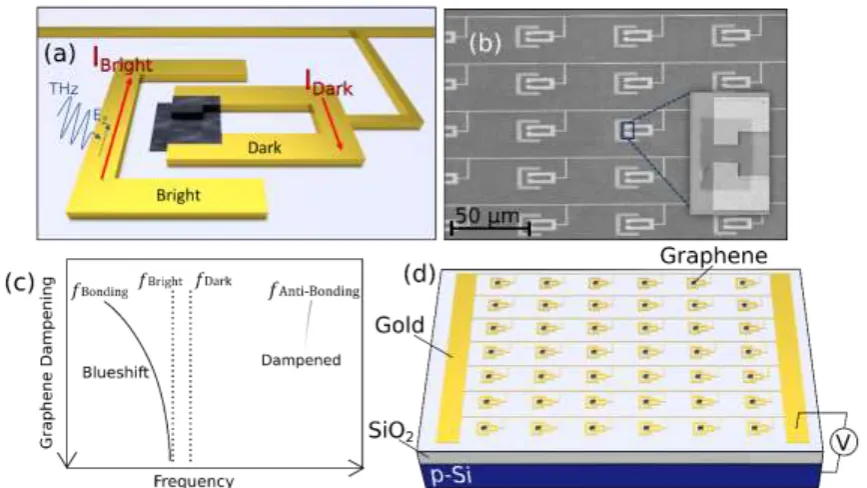
Figure 1. (a) Representation of coupled resonator structure. The arrows indicate the direction
of current flow for the bonding mode. (b) SEM image of resonator array. (c) Schematic illustration of the resonance frequency position of fBright and fDark. Showing how the resonance
frequency of fBonding is blue-shifted as the graphene dampening is increased and the resonance
at fAnti-Bonding is dampened. (d) 3D representation of the overall device architecture with back
gating. Ground is connected to the gold bond pads in this configuratoin.
The near-field capacitive coupling induces a splitting of the standard LSP resonances into two hybridized modes, with a low frequency ‘bonding’ resonance at fBonding and high frequency
‘anti-bonding’ resonance at fAnti-bonding. Figure 1a also describes the current in the resonators
when THz radiation with a frequency of fBonding is incident. A scanning electron microscope
(SEM) image of the device surface is shown in Figure 1b showing the repetition of the basic unit cell with graphene patches shorting the capacitive cap in the dark resonators.
[image:5.595.86.520.132.376.2]6
increases via electrostatic back gating, switching the metamaterial from a coupled resonator system, with a resonance at fBonding, to a single resonator LSP system, with a resonance at fBright.
For continuous tuning of the resonance frequency, the difference in frequency between fBonding
and fBright is designed to be small, which is achieved by lithographically designing the resonators
such that fBright < fDark. As a result, fBonding is continuously blue shifted towards fBright as the
graphene conductivity is increased, with only a minor impact on the Q factor. At the same time, the Q factor of the resonance at fAnti-bonding is quickly reduced as the graphene dampening
increases.
2.2. Device fabrication
The full device structure is illustrated in Figure 1d. Two separate devices, device 1 and device 2, are fabricated with different lithographic tunings. These devices have a bright resonator with total round-trip length of 38 µm and a dark resonator with round-trip length of 40.4 µm and 42.4 µm for device 1 and device 2 respectively. This was done to investigate how the relative sizes and LSP resonances (fBright and fDark) of the bright and dark resonators will influence the
coupling and tuning range of the device. Detailed device parameters are described in the supplementary information SI.1. These devices are fabricated on a boron p-doped silicon substrate with a 300 nm insulating layer of SiO2 to realize the electrostatic back gate. The total
7
biasing on a chip carrier configured to allow transmission measurements, with silver paste electrically contacting the p-doped silicon substrate to complete the back gate. A 1.2 mm x 1 mm adjacent graphene patch is shaped next to the device array on the same substrate for the electrical characterization of the graphene conductivity in the device as a function of back gate voltage. The same conductivity range measured from the uniform area has been assigned to the graphene arrays in the metamaterial devices, since the graphene growth and transfer, as well the processing have been carried out at the same time. This electrical characterization method is described in the supplementary information SI.2.
2.3. Electromagnetic finite element simulation
8
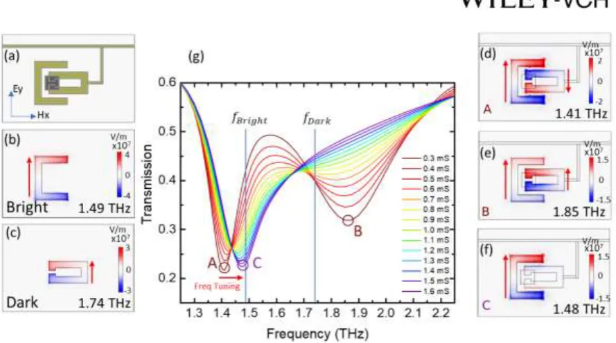
Figure 2. Simulation results for device 1. (a) Representation of cross section of unit cell and polarization of incident THz radiation. (b) and (c) describes the Ez field from the charge
carriers induced by the incident field on the bright resonator and dark resonator when they are not coupled. Ez field in the (d) bonding mode, (e) anti-bonding mode with graphene DC
conductivity set to 0.3 mS. (f) The single resonator LSP is retrieved when the graphene conductivity is set to 1.6 mS. The red arrows indicated the direction of current flow in each resonator. (g) COMSOL simulation of transmission through device 1 for different graphene conductivities.
The resonance condition for this coupled resonator structure is simulated using the same lithographic design parameters as device 1. Figure 2b and 2c describe the resonance conditions of the individual bright and dark resonators for device 1 when simulated separately. As discussed in the previous section, the dark resonator is designed to have a higher resonance frequency, 1.74 THz, than the bright resonator, 1.49 THz. This ensures that when these resonators are coupled together, the resultant bonding resonance at 1.41 THz is close enough to the bare bright resonator resonance, to allow for this resonance to be continuously tuned, as the coupled resonator system is changed to a single resonator system. The electric field in the Z direction, Ez, 20 nm above the metal surface is shown to describe the buildup and polarity of
9
The current induced in the bright resonator is 3 times higher than the dark resonator for the same incident power.
Figure 2d and 2e describe the electric field present for the hybridized bonding and anti-bonding resonances respectively when the resonators are capacitively coupled together and the DC graphene conductivity is set to 0.3 mS (a typical value for the graphene conductivity in these devices at the Dirac point)[22] with graphene induced losses at a minimum. The electric field is concentrated in the bright and dark resonators, despite the introduction of the thin metal biasing lines, confirming they are having a negligible effect on the resonance condition. The biasing lines do display a resonance at around 0.8 THz as shown in the supplementary information SI.5., however this is significantly far from the region of interest. For the bonding mode, the current in each resonator is rotating clockwise, whereas, for the anti-bonding mode, the current in the dark resonator is now rotating anti-clockwise. Figure 2f describes the resultant resonance condition at fBright when the DC graphene conductivity is at 1.6 mS (upper range of conductivity
achievable for the graphene in the device when biased away from the Dirac point) and the graphene induced dark resonator losses are high. There is a strong LSP resonance in the bright resonator which is similar to the isolated bright resonator case in Figure 2b and the electric field in the dark resonator is now an order of magnitude smaller, confirming that the coupling system has been transformed into a single resonator system.
10
transmission. As the graphene conductivity increases the anti-bonding resonance reduces quickly. The bonding resonance, however, being closer in frequency to fBright, is continuously
blue shifted until the single resonator resonance at fBright takes over. The Q factor (defined in
this case as the resonance width at transmission 0.35 divided by the center frequency) reduction throughout this process is minimal, which is an important feature for the utilization of these devices for practical applications, starting at ~10 for 0.3 mS and reducing to ~7 at 1.6 mS as the single resonator system dominates. From this simulation data, we would expect a continuous frequency tuning range of around 80 GHz for device 1 for a graphene conductivity tuning range of 0.3 mS to 1.6 mS.
3. Results
3.1. Transmission TDS
11
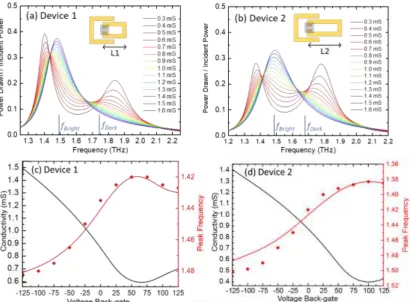
Figure 3. Transmission data using TDS system for (a) device 1 and (b) device 2 at different
back gate voltages. L1 = 18 µm and L2 = 17 µm.
Figure 3a shows the measured transmission curves through device 1 for different back gate voltages. From the electrical measurement of the DC graphene conductivity, the Dirac point was determined to be at ~60 V corresponding to a conductivity of 0.6 mS and with -125 V giving a maximum conductivity of 1.5 mS. When the graphene is most conductive, strongly dampening the dark resonator, the bright resonator frequency at 1.48 THz dominates. As the back gate voltage is increased towards the Dirac point, the conductivity reduces and the bonding resonance now becomes more pronounced, shifting the peak resonance frequency to ~1.42 THz. Throughout this transition, the Q factor remains above 7 and a total continuous frequency shift of ~60 GHz is observed. This experimental data for device 1 is in good agreement with the simulation data in Figure 2g with the resonance peaks accurate within 5 GHz and a similar tuning range achieved despite a smaller experimental graphene tuning range.
The same measurement was now performed on device 2 which has a unit cell with an identical sized bright resonator but a longer dark resonator, 18 µm instead of 17 µm. The dark resonator for device 2 supports a lower frequency LSP resonance than the dark resonator in device 1, 1.675 THz instead of 1.74 THz, according to simulation. This results in fDark being closer in
value to fBright which is 1.49 THz for both devices, and therefore a stronger coupling between
the resonators is achieved. The transmission measurement for device 2 for different back gate voltages is shown in Figure 3b. The Dirac point for device 2 is around 100 V with the graphene conductivity measured to be 0.4 mS. The maximum graphene DC conductivity for this device is measured to be 1.4 mS at -125 V. A similar variation in Dirac point positions between multiple devices has been observed and reported in other publications.[15] The available
12
in predicting precisely a priori the tuning range for the graphene due to small inconsistencies in preparation and fabrication.
The resonance frequency tuning range for device 2 is larger, displaying a frequency tuning range in the region of 120 GHz. The transmission through the device shows the resonance peak shifting from 1.38 THz to 1.50 THz as the voltage is swept from 100 V to -125 V. The stronger coupling between the two resonators, which are more matched in size, compared to device 1, results in fBonding being further from fBright and hence a larger shift in resonance frequency is
observed as the graphene conductivity is changed. However, this does not translate into a continuous frequency shift of the resonance, with the Q-factor changing much more than for device 1. There is, therefore, a trade-off between the overall tuning range and the smoothness of the transition between the bonding resonance and single LSP bright resonance illustrated by these two devices.
3.2 Equivalent circuit model
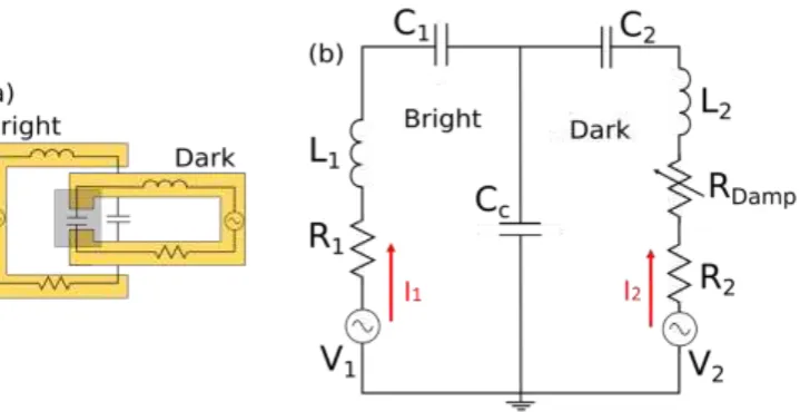
To further investigate the resonance condition of the coupled resonators as a function of frequency and graphene dampening, an equivalent lumped element circuit model is used. The individual resonators in isolation can be described as antennas which have a frequency dependent impedance described by an LCR electrical circuit as shown in Figure 4a. The coupling of the resonators is described by the two circuits connected via a parallel coupling capacitor as shown in Figure 4b. The AC voltage sources labeled V1 and V2 describe the
13
Figure 4. (a) Representation of two resonators as LCR circuits. (b) Resultant equivalent circuit
model of the coupled resonators.
The capacitors, C1 and C2, represent the energy stored in the electric field due to the buildup of
charges at each end of the resonators, for the bright and dark resonator respectively. The inductance values L1 and L2 describe the magnetic energy stored in the induced current in each
resonator with R1 and R2 describing the loss in the resonators. Extra induced loss by the
graphene patch in the dark resonator is described by an added variable resistor in series, RDamp.
The inductive qualities of graphene due to the complex impedance in the THz are negligible compared to the resonator inductance values and therefore it is sufficient only to consider the resistive loss of the graphene in the circuit model. The graphene patch will dissipate power and hence dampen the dark resonator according to the following equation.[45]
P𝐷𝑖𝑠𝑠 = σg‖EGap‖ 2
[image:13.595.124.484.77.262.2]14
As the dominant coupling effect comes from the electric field of charges in close proximity between the two resonators, the coupling is described as a parallel capacitive coupling, CC. The
power drawn, P𝐷𝑟𝑎𝑤𝑛, from voltage sources V1 and V2 was calculated in order to retrieve the
transmission, T, through the metamaterial device as this is proportional to the extinction coefficient and hence is proportional to |1-T|.[47] To estimate the power drawn, the current from each of the voltage sources as a function of angular frequency, 𝜔, is first derived from the following equations.
(𝑖1
𝑖2) = (𝑍)
−1(𝑉1
𝑉2) (2)
𝑍 = (
𝑅1+ 𝑗𝐿1𝜔 + 𝐶1+𝐶𝑐
𝑗𝜔𝐶1𝐶𝑐
1 𝑗𝜔𝐶𝑐
1
𝑗𝜔𝐶𝑐 𝑅2+ 𝑅𝐷𝑎𝑚𝑝+ 𝑗𝐿2𝜔 +
𝐶2+𝐶𝑐
𝑗𝜔𝐶2𝐶𝑐
) (3)
The current drawn from the voltage sources can be used to determine the time averaged power drawn as follows:
P𝐷𝑟𝑎𝑤𝑛 = 1/2Re(𝑉1𝑖1∗+ 𝑉2𝑖2∗) (4)
15
Figure 5. Power drawn from the voltage sources for different graphene conductivity values
using lumped element parameters derived for (a) device 1 and (b) device 2. The frequency of the coupling resonance as a function of back gate voltage for (c) device 1 and (d) device 2 (red points) in comparison with the frequency predicted using the lumped element model (red line). The measured conductivity as a function of back gate voltage is shown in black.
The model yields two coupled resonances, originating from the destructive interference between 𝑖1 and 𝑖2, in very good agreement with the COMSOL simulations and TDS results. The circuit model for device 1 accurately predicts the evolution of the coupled system into a single resonator system with a ~80 GHz blue shift of fBonding towards fBright which is
commensurate with the TDS data. The circuit model for device 2 shows a large binary shift of ~120 GHz fBonding and fBright and a 300 GHz shift between fAnti-bonding and fBright. This larger tuning
[image:15.595.97.509.86.388.2]16
symmetrical hybridization of the coupled resonances with fBonding and fBright further apart in
frequency.
The TDS measured bonding resonance frequency, as a function of back gate voltage, is plotted alongside the predicted values from the corresponding circuit models in Figure 5c and 5d. The electrical measurements are also shown, describing the graphene conductivity as a function of back gate voltage. Despite the simplicity of the circuit model, the TDS data lines up well, particularly for device 1 which has well-defined resonance positions for the full range of back gate voltages. The model also predicts the increased tuning range for device 2 as the resonators are more closely matched in resonant frequency. This circuit model technique could, therefore, be a useful design tool for future devices and for further optimization of the device structure.
3.3 Group delay measurement
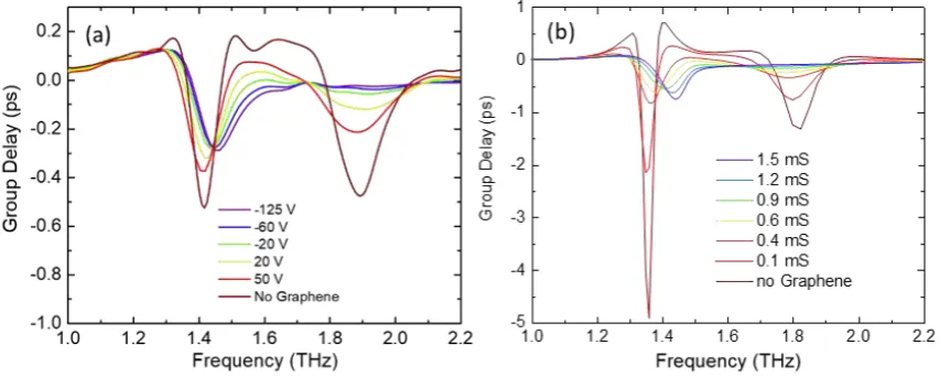
The EIT phenomena present in these devices is accompanied by an extreme modification of the dispersion properties which leads to the slow light effect due to an alteration of the group velocity through the device. The ability to actively control slow light through a device could have implications for fundamental scientific research as well as the implementation of optical techniques such as slow light buffers. To quantify this phenomenon in these devices, the group delay, 𝛥𝑡𝑔, described as the time delay of a THz wave packet through the sample in comparison to air, is determined by the following equation:
𝛥𝑡
𝑔=
𝑑∅𝑑𝜔 (5)
17
The experimental data using device 1 is accompanied by data using an identical device with no graphene present to determine the group delay when there is no graphene dampening.
Figure 6. (a) Measurement of group delay through device 1 using phase data from TDS for
different back gate voltages. (b) Simulation of Group delay using COMSOL simulation for different graphene conductivities.
[image:17.595.87.514.146.317.2]18 4. Conclusion
In conclusion, EIT active devices, based on the interplay between graphene and coupled resonator metamaterial arrays, have been successfully demonstrated for operation in the THz frequency range. Two different designs have been realized and fully characterized via a THz-TDS system, showing a frequency tuning of the resonance by 60 GHz and 120 GHz respectively. The former device would be particularly useful as a fast, continuously tunable, frequency band reject filter in the THz region with the later device, better suited as a binary switchable frequency filter. Due to the reconfigurable dispersion properties of these devices, they could also be implemented for group delay tuning for slow light applications. The group delay values are commensurate with other proposed EIT metamaterial designs which use photo-active modulation components,[48] however, the design in this paper has the advantage of being electrically switchable. For implementation with THz QCLs, these devices can be scaled down in size to work above 2 THz and can readily be used in an external cavity in an experimental configuration similar to reference [22], opening up a range of applications for spectroscopy and communications.
Supporting Information Supporting Information is available from the Wiley Online Library or from the author.
Acknowledgments
SJK acknowledges IPES CDT for funding and support. SJK, NA, BW, RW, WM, VSK, HEB, DAR and RD acknowledge financial support from the Engineering and Physical Sciences Research Council (Grant No. EP/P021859/1, Hyper Terahertz). WM thanks the George and Lillian Schiff Foundation of the University of Cambridge for financial support and is grateful for the Honorary Vice-Chancellor's Award of the Cambridge Trust. RD acknowledges support from Teranet network grant (EP/M00306X/1) and from the Royal Society (RSG\R1\180148 - Research Grant). SH acknowledges funding from EPSRC (EP/K016636/1). P.B.W.
acknowledges EPSRC Cambridge NanoDTC (EP/G037221/1).
19 References
[1] S. S. Dhillon, M. S. Vitiello, E. H. Linfield, A. G. Davies, M. C. Hoffmann, J. Booske, C. Paoloni, M. Gensch, P. Weightman, G. P. Williams, E. Castro-Camus, D. R. S. Cumming, F. Simoens, I. Escorcia-Carranza, J. Grant, S. Lucyszyn, M. Kuwata-Gonokami, K. Konishi, M. Koch, C. A. Schmuttenmaer, T. L. Cocker, R. Huber, A. G. Markelz, Z. D. Taylor, V. P. Wallace, J. A. Zeitler, J. Sibik, T. M. Korter, B. Ellison, S. Rea, P. Goldsmith, K. B. Cooper, R. Appleby, D. Pardo, P. G. Huggard, V. Krozer, H. Shams, M. Fice, C. Renaud, A. Seeds, A. Stöhr, M. Naftaly, N. Ridler, R. Clarke, J. E. Cunningham, and M. B. Johnston. J. Phys. D: Appl. Phys. 2017, 50, 043001.
[2] J. Faist, F. Capasso, D. L. Sivco, C Sirtori, A. L. Hutchinson, A. Y. Cho, Science 1994, 264, 553.
[3] R. Köhler, A. Tredicucci, F. Beltram, H. E. Beere, E. H. Linfield, A. G. Davies, D. A. Ritchie, R. C. Iotti, F. Rossi. Nature 2002, 417, 156.
[4] D. Grischkowsky, S. Keiding, M. V. Exter, C. Fattinger. J. Opt. Soc. B 1990, 7, 2006. [5] M. V. Exter, C. Fattinger, D. Grischkowsky, Opt. Lett. 1989, 14, 1128.
[6] M. Rahm, J. S. Li, W. J. Padilla, J. Infrared Millim. Terahertz Waves 2013, 34, 1.
[7] R, Degl’Innocenti, S. J. Kindness, H. E. Beere, D. A. Ritchie, Nanophotonics 2018, 7, 127. [8] W. J. Padilla, A. J. Taylor, C. Highstrete, M. Lee, R. D. Averitt, Phys. Rev. Lett. 2006, 96,
107401.
[9] S. Zhang, J. Zhou, Y. S. Park, J. Rho, R. Singh, S. Nam, A. K. Azad, H. T. Chen, X. Yin, A. J. Taylor, X. Zhang, Nat. Comms. 2012, 3, 942.
[10]J. Zhou, D. R. Chowdhury, R. Zhao, A. K. Azad, H. T. Chen, C. M. Soukoulis, A. J. Taylor, J. F. O’Hara, Phys. Rev. B 2012, 86, 035448.
[11]J. Gu, R. Singh, X. Liu, X. Zhang, Y. Ma, S. Zhang, S. A. Maier, Z. Tian, A. K. Azad, H. T. Chen, A. J. Taylor, Nat. Comms. 2012, 3, 1151.
20
[13]Y. Yao, M. A. Kats, R. Shankar, Y. Song, J. Kong, M. Loncar, F. Capasso, Nano. Lett. 2013; 14, 214.
[14]P. Q. Liu, I. J. Luxmoore, S. A. Mikhailov, N. A. Savostianova, F. Valmorra, J. Faist, G. R. Nash, Nat. Commun. 2015, 6, 8969.
[15]R. Degl’Innocenti, D. S. Jessop, Y. D. Shah, J. Sibik, A. Zeitler, P. R. Kidambi, S. Hofmann, H. E. Beere, D. A. Ritchie, ACS Nano 2014, 8, 2548.
[16]D. S. Jessop, S. J. Kindness, L. Xiao, P. Braeuninger-Weimer, H. Lin, Y. Ren, C. X. Ren, S. Hofmann, A. Zeitler, H. E. Beere, D. A. Ritchie, Appl. Phys. Lett. 2016, 108, 171101. [17]D. K. Efetov, P. Kim, Phys. Rev. Lett. 2010, 105, 256805.
[18]L. Ju, B. Geng, J. Horng, C. Girit, M. Martin, Z. Hao, H. A. Bechtel, X. Liang, A. Zettl, Y. Shen, Nat. Nanotech. 2011, 6, 630.
[19]P. A. Huidobro, M. Kraft, S. A. Maier, J. Pendry, ACS Nano 2016, 10, 5499. [20]P. Q. Liu, F. Valmorra, C. Maissen, J Faist, Optica 2015, 2, 135.
[21]Y. Fan, N. Shen, F. Zhang, Q. Zhao, Z. Wei, P. Zhang, J. Dong, Q. Fu, H. Li, C. M. Soukoulis, ACS Photonics 2018, 5, 1612.
[22]S. J. Kindness, D. S. Jessop, B. Wei, R. Wallis, V. S. Kamboj, L. Xiao, Y. Ren, P. Braeuninger-Weimer, A. I. Aria, S. Hofmann, H. E. Beere, D. A. Ritchie, R. Degl‘Innocenti Sci. Rep. 2017, 7, 7657.
[23]B. Wei, S. J. Kindness, N. W. Almond, R. Wallis, Y. Wu, Y. Ren, S. C. Shi, P. Braeuninger-Weimer, S. Hofmann, H. E. Beere, D. A. Ritchie, R. Degl’Innocenti, Appl. Phys. Lett. 2018, 112, 201102.
[24]S. Zhang, D. A. Genov, Y. Wang, M. Liu, X. Zhang, Phys. Rev. Lett. 2008, 101, 047401. [25]N. Papasimakis, V. A. Fedotov, N. I. Zheludev, S. L. Prosvirnin, Phys. Rev. Lett. 2008, 101,
253903.
21
[28]Z. Li, Y. Ma, R. Huang, R. Singh, J. Gu, Z. Tian, J. Han, W. Zhang, Opt. Express 2011, 19, 8912.
[29]Y. Ma, Z. Li, Y. Yang, R. Huang, R. Singh, S. Zhang, J. Gu, Z. Tian, J. Han, W. Zhang, Opt. Mat. Express 2011, 1, 391.
[30]Q. Bai, C. Liu, J. Chen, C. Cheng, M. Kang, H. T. Wang, J. Appl. Phys. 2010, 107, 093104. [31]K. Zhang, C. Wang, L. Qin, R. W. Peng, D. H. Xu, X. Xiong, M. Wang, Opt. Lett. 2014,
39, 3539.
[32]L. V. Hau, S. E. Harris, Z. Dutton, C. H. Behroozi, Nature 1999, 397, 594. [33]I. Novikova, R. L. Walsworth, Y. Xiao, Laser Photonics Rev. 2012, 6, 333. [34]H. Schmidt, A. Imamoglu, Opt. lett. 1996, 21, 1936.
[35]Y. Wu, J. Saldana, Y. Zhu, Phys. Rev. A 2003, 67, 013811.
[36]N. Liu, T. Weiss, M. Mesch, L. Langguth, U. Eigenthaler, M. Hirscher, C. Sönnichsen, H. Giessen, Nano Lett. 2010, 10, 1103.
[37]G. D. Liu, X. Zhai, L. L. Wang, Q. Lin, S. X. Xia, X. Luo, C. J. Zhao, Plasmonics 2018, 13, 15.
[38]C. Y. Chen, P. H. Hsiao, J. Phys. D: Appl. Phys. 2016 , 49, 135101.
[39]M. M. Jadidi, A. B. Sushkov, R. L. Myers-Ward, A. K. Boyd, K. M. Daniels, D. K. Gaskill, M. S. Fuhrer, H. D. Drew, T. E. Murphy, Nano letters 2015, 15, 7099.
[40]Z. Chen, J. Chen, Z. Wu, W. Hu, X. Zhang, Y. Lu, Appl. Phys. Lett. 2014, 104, 161114. [41]Q. Fu, F. Zhang, Y. Fan, J. Dong, W. Cai, W. Zhu, S. Chen, R. Yang, Appl. Phys. Lett.
2017, 110, 221905.
[42]Y. Fan, T, Qiao, F. Zhang, Q. Fu, J. Dong, B. Kong, H. Li, Sci. Rep. 2017, 7, 40441. [43]P. Braeuninger-Weimer, B. Brennan, A. J. Pollard, S. Hofmann, Chem. Mater. 2016, 28,
8905.
22
[46]Q. Li, L. Cong, R. Singh, N. Xu, W. Cao, X. Zhang, Z. Tian, L. Du, J. Han, W. Zhang, Nanoscale 2016, 8, 17278.
[47]M. Amin, M. Farhat, H. Baǧcı. Sci. Reports 2013, 3, 2105.
[48]F. Miyamaru, H. Morita, Y. Nishiyama, T. Nishida, T. Nakanishi, M. Kitano, M. W. Takeda. Sci. Reports 2014, 4.