I. Abstract
Two-dimensional (2D) materials hold immense potential for both improvement of current
technologies and employment in novel technology due to the alterations of material properties as
size transitions from the macroscopic to nanoscopic state where quantum-confined states emerge.
While some 2D materials have already been investigated, such as graphene, MoS2, and a few
ultrathin transition metal oxide films, many of these materials are prepared via exfoliation or
other physical breakdown methods of a bulk material with a few grown by CVD with low
structural control. The class of materials where this is experimentally demonstrated is rather
restricted in scope, and exfoliation methods are limited in product yield. In this study, I present a
scalable method for general fabrication of 2D metal oxide materials through atomic layer
deposition (ALD) using oriented ionic substrates. This study seeks to expand the availability of
2D materials by determining a fabrication method that would only be limited by the availability
of ALD precursor materials and could be easily scaled to the size of the substrate. TiO2 was
selected as a model system to fabricate for its practical usefulness and versatility in a number of
applications such as catalysis and photovoltaic devices. Ultraflat, single-crystal NaCl slabs were
chemically-treated and used as substrates for ALD TiO2 fabrication, employing only the (100)
NaCl surface. A custom-designed “saturation-pulse deposition” (SPD) process was used to
deposit the Ti precursor and fabricate the film. After deposition, the system was spin-coated with
polypropylene carbonate (PPC) and the film was lifted off the NaCl substrate in a basin of
ultrapure DI water, selectively dissolving the ionic substrate and allowing the resulting material
to be isolated and transferred to a substrate of choice.
II. Introduction
produced a mechanically-strong material with phenomenal electrical and optical properties at
single-atom thickness.1 Since this discovery, research into graphene and its interesting 2D
properties has exploded, challenging previous notions of charge transport limitations and
electronics applications2 as well as prompting the search for other 2D materials. As interest in graphene’s size-quantized properties grew, other layered materials such as MoS2 and hBN
became subjects for further exploration of new 2D semiconductors and insulators, respectively.3 In almost all of these cases, the quantum-confinement size effects present in 2D materials
provides significant improvement over bulk properties. Many of these materials have since been
noted for their uses in solar cells,4 charge transport layers,5 and photoconversion layers,6 all employing significantly improved properties compared to their bulk counterparts. However,
despite this interest and the progress over the last decade, the number of 2D materials with facile
synthetic routes is still limited to only a few structural and material types. Furthermore, these
synthetic routes typically employ a top-down method such as exfoliation of a bulk material into
nanosheets;7 2D materials only uncommonly fabricated directly through a bottom-up approach. With highly desirable properties such as a tremendous amount of control of the fabrication
process itself and structural control over the final material, a bottom-up approach offers a
significant advantage over top-down methods. In order to increase the number of synthetically
obtainable 2D materials, bottom-up approaches offer the potential to fabricate many different
material systems.
For these purposes, ALD is an attractive fabrication method. Particularly, ALD can be
used with many different precursor materials and allows for large amounts of control over
surface morphology, where the deposited material fully coats the substrate and conforms to the
vapor deposition (CVD) growth for similar purposes,9 but ALD- a subsection of CVD- offers unparalleled structural control. For purposes of 2D material fabrication, this type of growth
model is crucial in order to obtain a flat film across the entire substrate rather than a granule of
material. Growth through ALD is self-limited;10 the reaction proceeds to thermodynamic completion as the deposited material reaches a constant maximum value for every cycle and
ceases deposition of additional material. By introducing a self-limiting mechanism, atomic
control of the film thickness is achieved, giving a significant amount of spatial control of film
growth. In addition to these, ALD can be used for a variety of different precursors8,11 and substrates,12 demonstrating its practical selection for the synthesis of 2D material systems. In addition to this level of versatility, ALD creates films of high-quality under mild reaction
conditions, accompanied with surface chemistry conducive for electronics applications,13 making it appealing for ensuring film stability and strength throughout fabrication. Combined, the
versatility of accommodating numerous materials and substrates, the high quality of deposited
materials, and the self-limited reaction conditions provide strong support for ALD use in 2D
material fabrication.
Because of their intrinsic flatness, ionic substrates have been used for epitaxial film
growth for almost 50 years14 for a variety of materials, these properties are again being leveraged
here in ALD for 2D material fabrication. Cleaved ionic substrates represent a cost-effective and
simple means to create substrates with specific crystal planes exposed as well as intrinsically flat
surfaces from cleavage along these planes. Cleavage along a crystal plane only exposes that
crystal plane, and the preferential orientation of the plane induces a particular structure in the
deposited material, acting as a template15 and influencing the assembly behavior of any material
material, as even the smallest of deviations from the desired structure can dramatically alter or
destroy the film.
Oriented NaCl substrates were used for the deposition of TiO2 films to take advantage of
these substrate properties. We used Ti precursors as a deposition material with the intent of
fabricating TiO2 as an end product due to its wide range of potential applications and
well-understood behavior. TiO2 has been characterized in different morphologies for practical
applications17 and the effects of deposition techniques on structure of the final material are well
understood.18 In choosing a well-behaved, well-understood material, appropriate focus can be given to development of the 2D fabrication process itself rather than to one specific material.
Here, we explore the ALD synthesis of a 2D metal oxide, TiO2, on atomically flat ionic
substrates, NaCl (100), followed by investigating the ability to transfer the 2D film to other
substrates. At present, the thinnest ALD film ever successfully transferred has been
approximately 50 nm thick, and the material possessed a wrinkled structure.19 In contrast, a fabricated monolayer would be thinner by a factor of one hundred, much thinner than any
previous work. With the level of structural control offered by ALD, alternative structures, such
as engineered defects or other irregularities, may be possible in future work, leading to
applications in advanced technology such as molecular membranes. Successful fabrication of a
single layer material may also be repeated, a valuable route to creating stacked 2D
heterostructures. By developing this bottom-up 2D material fabrication process in a general
sense, the potential applications of 2D materials increases exponentially.
III. Methods
A. Substrate Design
>99.9% purity. Substrates were cleaved along the (100) plane from the larger crystal using a
hammer and new razor blade, inspecting cleaved substrates for large defects. The newly cleaved
surface then becomes the active surface for the entire 2D fabrication. As-cleaved NaCl substrates
were then immediately placed in a ceramic boat and inserted into a quartz tube for a Thermo
Scientific Lindberg Blue M tube furnace for thermal annealing, to further flatten the surface. The
substrates were placed under an inert N2 atmosphere and annealed at 600°C, with a 6 hour
ramp-up time from room temperature, 14 hours at 600°C, and 10 hours of cooling to room
temperature. All N2 was filtered through a Drierite in-line filter to ensure the N2 is devoid of
moisture. Once the samples were removed from the furnace, they were analyzed immediately.
Substrate contact with open air was minimized to prevent surface condensation of water; all
samples are stored in a desiccator.
B. ALD Deposition
ALD has been heavily studied for similar uses in metal thin film growth,11 and these principles are applied nearly identically to our system using a Cambridge Nanotech Savannah
S200 ALD instrument. Because ALD is thermodynamically limited rather than a kinetically, the
deposition conditions cause the reaction between the gaseous precursor materials and the
substrate surface to proceed to full thermodynamic completion; this means the entire substrate
surface is coated with a uniform single layer of the precursor material, without gaps or overlap.
Once the NaCl substrates had been annealed, they were immediately used for ALD studies to
minimize condensation and surface contamination. The ALD process proceeds in vacuum at
approximately 0.02 Torr, with a valve manifold temperature set to 150°C, inner/outer chamber
temperatures both set to 200°C, and jacket heater at 75°C for the Ti precursor. For the 2D metal
and closing of the stop valve before each pulse of water or precursor material to ensure all
material remains in the reactor with the substrate and saturates the chamber. The pulsed materials
were allowed to react with the substrate for a portion of time before opening the stop valve and
returning N2 flow, flushing the chamber (full method available in Appendix 1). This process is
repeated both for the water pulse and the metal precursor pulse one time, allowing for the growth
of only one atomic layer of a metal oxide film.
C. Transfer from NaCl
Lift-off methods for epitaxial films have been previously established, employing a
weakly bonded ionic layer between the substrate and film of interest that could then be removed
by mechanical fracturing.20 However, mechanical fracturing of the deposited 2D material from the substrate would likely destroy the atomically thin material in the process, necessitating an
alternative method to isolate and transfer it. In our study, rather than use an intermediate ionic
layer, the film was deposited directly on the ionic substrate, allowing similar advantages and
simplifying the system. Next, a PPC film was spin-coated using a 10% weight solution of PPC in
ethyl acetate at 2500 rpm for 60s and the PCC/TiO2/NaCl sample was dried on a hot plate. To
remove the substrate, the sample was floated on a basin of 18 MΩ•cm nanopure DI water,
advantageously using the buoyancy of the polymer and the surface tension of the water so the
NaCl substrate is submerged while the PPC surface remains dry. The ionic substrate dissolves
fully, leaving behind only the 2D metal oxide film and polymer, which remain floating. The
basin is then drained slowly, lowering the buoyant film and polymer onto a substrate of choice.
The film is washed by repeatedly floating the TiO2/PPC film on clean DI water applied to the
new substrate and removal of water with a pipette followed by drying in a vacuum oven at 125°C
D. Characterization: AFM and XPS
Because of the incredibly small dimensions of 2D materials, studies of the substrate
cleavage, thermal annealing, material deposition, and transfer verification all require
surface-level analysis techniques, particularly atomic force microscopy (AFM) and X-ray photoelectron
spectroscopy (XPS). All AFM studies were performed on an Asylum Research MFP3D Atomic
Force Microscope in tapping mode for surface roughness and topography measurements. Scan
sizes of both 20 µm2 and 10 µm2 are used for survey and focused topographies, respectively,
with the instrument calculating RMS roughness values of the scan. All XPS studies were
performed on a Kratos Axis Ultra DLD X-ray photoelectron spectrometer outfitted with a
monochromatic Al Kα source of core electrons, collecting chemical signatures from the
fabricated film as well as any noticeable shifts in these signatures.
IV. Results and Discussion
Current top-down methods of creating 2D materials use a bulk material, a liquid
subphase, and some exfoliation method, to create thickness dispersion solutions of 2D flakes.21 Exfoliation methods yield limited little control of flake thickness, shape, size, or integrity. In
contrast, a bottom-up fabrication method of 2D materials, such as the one presented here,
provides precise control over all aspects of the material system, including the deposition process,
the substrate design, and the 2D film composition
Ionic substrates offer advantages of low-energy crystal planes- both as oriented surfaces
for 2D film deposition and the cleavage plane for an atomically flat surface. Cleavage along
these planes guarantees a perfectly clean surface, free of airborne particulates and adsorbed water
at the moment of cleavage. Immediately after cleavage, the pristine surface is examined using
single plane using only simple tools remains a near-impossible feat and many atomic plane edges
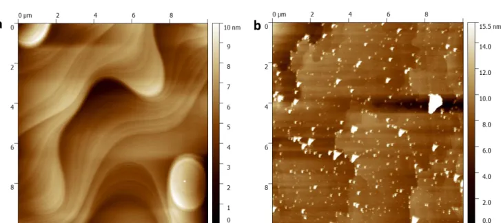
were seen, along with defects and a nonlinear surface topology (Figure 1a). To flatten this
surface corrugation, a thermal annealing process in open air to 600°C, within 50°C of NaCl
melting point, was performed for all ionic substrates immediately after cleavage. While thermal
annealing thoroughly flattened the variance in surface topology and many of the atomic plane
edges, it also caused the appearance of particulates on the surface of the substrate (Figure 1b).
Figure 1. (a) Topography of NaCl substrate as-cleaved. (b) Topography of NaCl substrate cleaved and annealed in open-air.
These particles have a preferential nucleation on the atomic plane edges and corners, with
a triangular morphology and similar orientations across the sample. The congruity in these two
parameters across particles likely indicates one type of growth reaction is occurring and that
reaction prefers to occur on certain facets of the NaCl substrate, such as edge states. These
particles are attributed to high-temperature reactions of the NaCl with water, CO2, and
hydrocarbons naturally found in air during annealing, possibly resulting in Na2CO3 island growth
on the surface. The quartz tube from the furnace also may be a source of contamination, as
quartz also can undergo a high temperature reaction with water, producing SiO2, which may
deposit on the ionic substrate. Additionally, impurities in the NaCl substrate migrate to the
a
.
surface due to their high mobility in the crystal at temperatures approaching the melting point of
NaCl, aggregating on the surface as impurity particles intrinsic to the substrate. Adsorbed surface
matter is significantly reduced by annealing under dry N2 conditions. By annealing in inert, dry
N2, the high-temperature side reactions of NaCl with molecules found in air as well as any
water-based reactions are suppressed, drastically minimizing surface contamination. However, a few
Figure 2. (a) Topography of NaCl substrate annealed under N2. (b) Sample height profile across atomic plane reported for line shown in (a).
particles are still seen from impurities in the starting NaCl crystal (Figure 2). After annealing the
NaCl substrates under N2, only a few atomic planes are seen through AFM analysis, yielding an
overall RMS roughness value of 219.5 pm, similar to the RMS roughness for a clean, atomically
flat Si wafer. Even with the atomic plane edges exposed, each plane only has a height of
approximately 300 pm, contributing little overall roughness to the substrate.
With prepared, atomically-flat, ionic substrates, a 2D TiO2 film can be fabricated using
an ALD process. We first conducted a proof-of-concept study in order to develop and validate
the deposition process independently of the ionic substrate design. The deposition process,
termed “saturation-pulse deposition” (SPD) consisted of isolating the reactor chamber in 0
0.1 0.2 0.3 0.4
0 0.5 1 1.5 2
H
eight
(n
m
)
Distance (µm)
b
.
a
sufficient time to react and deposit on the substrate surface. Because ALD processes are
thermodynamically self-limited, allowing precursor material to be in excess of the reaction
results only in full coverage of the substrate surface. All excess precursor material was then
evacuated from the chamber in a later step. In essence, the deposition process is engineered such
that the entire substrate surface is uniformly coated with a monolayer of TiO2, fully exploiting
the structural control offered by ALD.
Once developed, the SPD process could be applied to Si substrates since these substrates
are well-suited for metal oxide ALD with their atomically-flat surfaces. Furthermore, the use of
Si substrates allowed for easy comparison of samples and assessment of general uniformity of
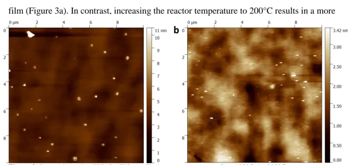
the resulting TiO2 films. Initially, the deposition was performed at low reactor temperatures of
120°C, resulting in nanoparticles of TiO2 on the substrate rather than a uniform and homogenous
film (Figure 3a). In contrast, increasing the reactor temperature to 200°C results in a more
Figure 3. Deposition using SPD for TiO2 on Si, reactor temperature of (a) 120°C (b) 200°C.
conformal TiO2 film, with only a few nanoparticles of much smaller size (Figure 3b). By
increasing the reactor temperature, the excess thermal energy aids in overcoming the energetic
barrier to wetting, allowing a full aqueous film coverage of the substrate surface for later reaction
with volatile Ti precursor molecules, ultimately creating a single layer film.
a
.
Thin 2D films, especially at thicknesses approaching monolayers, are rather difficult to
characterize due to the small amount of material. Often, detection of these materials requires
surface-sensitive techniques, or taking advantage of the material’s unique optoelectronic
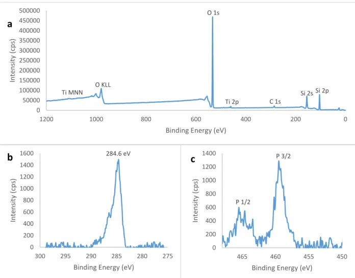
properties.22 For this study, Raman spectroscopy and energy dispersive spectroscopy (EDS) did not possess high enough sensitivity to identify monolayers of a material. Instead,
surface-sensitive XPS was used to confirm deposition of TiO2 onto Si substrates (Figure 4). In these XPS
Figure 4. (a) Survey spectra for TiO2 saturated pulse on Si. (b) C 1s core electron reference. (c) Ti 2p core electron, corrected to adventitious carbon.
results, small but noticeable peaks arise between 455 and 470 eV binding energies,
corresponding to the binding energy of core electrons in the p-orbitals of Ti species. These peaks
act as chemical “fingerprints” for Ti species, confirming the deposition on the surface of the Si
Ti MNN
O KLL
O 1s
Ti 2p C 1s
Si 2s Si 2p
0 50000 100000 150000 200000 250000 300000 350000 400000 450000 500000 0 200 400 600 800 1000 1200 In ten sity (cp s)
Binding Energy (eV)
284.6 eV 0 200 400 600 800 1000 1200 1400 1600 275 280 285 290 295 300 In ten sity (cp s)
Binding Energy (eV)
P 1/2 P 3/2 0 200 400 600 800 1000 1200 1400 450 455 460 465 In te n sity (cps )
substrate even at incredibly small amounts of material such as monolayers. Additionally, Ti
peaks present from SPD deposition show small shifts toward higher binding energy compared Ti
peaks from bulk TiO2, shifting from a bulk value of 464.3 eV to 465.5 eV for the p1/2 peak and
from 458.5 to 459.5 eV for the p3/2 peak.23 This binding energy shift may indicate quantum
confinement effects due to the material’s inherent 2D structure.
Although XPS determined the presence of TiO2 at low amounts, it yields little
information about the actual structure of the material itself. We then examined structural
conformity of the 2D film and its Si substrate. A sample of bare, cleaned Si was examined in
AFM for reference, giving an intrinsic RMS roughness value of 210.5 pm for the substrate as
well as a topology (Figure 5a). The deposited TiO2 film was characterized, yielding an RMS
roughness value of 250.8 pm (Figure 5b). Based on the remarkable similarity between RMS
roughness values of Si and deposited TiO2 film and the nearly identical topographies across
Figure 5. AFM scans of (a) Reference spectra of bare Si wafer, (b) As-deposited 2D TiO2 on Si wafer
the entire TiO2 film, the 2D metal oxide is assumed to deposit as a conformal film across the
entire Si surface. Few particles are seen on the as-deposited surface, with the few potential
nanoparticles being incredibly small. Additionally, some small particulates are seen even on the
surface of the bare wafer, indicating that they likely arise from contamination of the
a
.
surroundings rather than from deposition. Combining the AFM images of the as-deposited films
on Si and the XPS results of those films, it can be concluded that deposition successfully occurs,
and the deposited material conforms to the substrate as a film.
The SPD process was then coupled to the ionic substrate design, resulting in deposition
of the 2D material onto the intended NaCl substrates. The deposition process was not altered, as
substrate change should not affect deposition. Ionic substrates may offer a small advantage
compared to Si substrates as they are very hydrophilic, causing the water deposition step to fully
wet the surface with a very small energetic penalty. As a result, the SPD process results in a
similarly conformal film when applied to ionic substrates (Figure 6) while maintaining a
sub-nanometer level RMS roughness of 752.8 pm for the 2D film. Notably, AFM images of SPD
Figure 6. (a) AFM image of TiO2 deposited on NaCl substrate. (b) Sample height profile reported from line in (a). deposition onto NaCl substrates show small particles adsorbed to the surface, possibly small
nanoparticles. However, as previously shown, these particles are present in all samples using
ionic substrates, as they are also seen before deposition and are attributed to crystal impurities
rather than deposition issues.
0 0.2 0.4 0.6
0 0.5 1 1.5 2
H
eight
(n
m
)
Distance (um)
Profile of TiO2 Saturated
Deposition on NaCl
b
.
a
Finally, once the deposition onto the treated substrates was completed, the film was
isolated and transferred off of the ionic substrate. We accomplished the transfer from the original
sacrificial substrate by spin-coating a polymer on top of the TiO2 film (Scheme 1a) and floating
the material system in a basin of ultrapure DI water (Scheme 1b). Then, we drained the basin
after the substrate dissolved, and deposited it onto a new substrate (Scheme 1c). Finally, we
removed of the polymer with acetone and isopropyl alcohol (Scheme 1d). Using such a method
relies on the surface tension interaction and buoyancy considerations of the polymer relative to
Scheme 1. Transfer mechanism for 2D film. (a) Spin coating as-deposited film with desired polymer. (b) Floating system onto DI water surface, dissolving NaCl substrate. (c) Draining the basin, lowering film and polymer onto new substrate. (d) Polymer removal for final film.
the basin of water. Under normal circumstances, both NaCl and TiO2 in their solid states sink in
water; however, the addition of PPC polymer with much lower density than the substrate or the
TiO2 film, the sample experiences an increased buoyance. Since the polymer is hydrophobic in
nature, it results in increased interfacial surface energy between the water and polymer. With this
surface tension, the material system can float, allowing for the dissolution of the ionic substrate
easily. Furthermore, delamination while submerged results in the PPC/TiO2 film rapidly
d
.
c
.
b
.
a
surfacing, a rather unpredictable process that may put the film under strain.
Polymer selection for the transfer process is an important choice, integral to the
successful transfer of 2D TiO2 films. A polymer must be selected such that the deposited
material preferentially adheres to the polymer over the ionic substrate during substrate
dissolution to prevent loss of the film. Additionally, the polymer must not adhere to the film so
strongly that the film breaks under the tension, creating a balancing act between to facilitate a
successful transfer. A polymer such as poly-dimethylsiloxane (PDMS) has extended methyl
groups, offering little adhesion to oxide surfaces and allowing for nearly instant delamination
from the ionic substrate and film. In contrast, a polymer such as poly-methyl methacrylate
(PMMA) adheres to TiO2 through multiple oxygen groups, all of which can bind to the film
surface. Because PMMA binds so tightly to the film, it causes mechanical tension that may
damage the film, making it an inappropriate choice for polymer selection. In this study, PPC was
selected as the polymer due to its limited, but still present, adhesion interactions through its
exposed oxygen groups. These groups would adhere to the 2D oxide surface of the film weakly,
allowing it to be transferred to a new substrate without destroying the fabricated 2D material.
After polymer selection, transferring the 2D material onto a new substrate requires only a
mechanical process along with a washing step. After dissolution of the ionic substrate, the water
basin is drained, lowering the film and polymer combination onto a new substrate of choice. The
new system is repeatedly washed with clean DI water to remove any remaining ions from the
NaCl substrate, using the capillary effects between the film and substrate to “pull” water between
first by pipet and then dried in a vacuum oven. Polymer was then by removed with acetone and
IPA or pyrolysis. Once polymer was removed, the final 2D TiO2 film was exposed.
After the transfer process has been completed, the only material present is the fabricated
2D oxide film on the new transfer substrate. However, despite our success designing a substrate
developing an efficient deposition process, the polymer selection of the fabrication process
remains a roadblock to successful fabrication of the material in a transferrable fashion. Under
current conditions, the TiO2 film does not adhere to the PPC polymer during transfer, resulting in
the loss of the film in the water basin. Since we previously confirmed successful deposition
through XPS, and no Ti signatures can be seen for the film after the transfer, the film must be
lost in the transfer process. However, the transfer process remains robust in that no wrinkling or
other destruction to the film/polymer combination occurs, and the surface tension causes the
polymer to remain taught across the air/water interface. Given these circumstances, the polymer
selection only needs to be fine-tuned to the film material to ensure better adhesion to result in a
successful transfer process. With this final step, bottom-up fabrication of a 2D metal oxide
material will be successfully demonstrated.
V. Conclusions and Future Work
In this work, the feasibility of using ALD for fabrication of 2D TiO2 films on oriented
ionic substrates that can be isolated and transferred is demonstrated. Thermally annealed cleaved
NaCl substrates form a template for orienting film growth while ALD reaction conditions are
tuned for saturation coverage during material deposition. Thus, high-quality crystalline 2D films
can be fabricated on these substrates, taking advantage of saturation conditions during ALD
fabrication. Once polymer is spin-coated over the film and substrate, the film preferentially binds
ALD deposition process is confirmed through XPS analysis of the sample, specifically Ti
signatures, as is the successful transfer of the material to a new substrate during float-off
procedures. AFM imaging is also used to note the physical structure and topology of the newly
fabricated material relative to the topology of the bare substrate, and to confirm the integrity of
the film after transfer. This approach could be used for many applications of 2D materials, as the
resulting film can be added to any desired substrate or already existing material system during
the transfer process. Future work in this study lies mostly in generalizing the fabrication process
to other metal oxide 2D materials- ensuring the process is robust and applicable throughout the
material class. Furthermore, the polymer coating can be fine-tuned for selective film adhesion
across different materials, fully binding the material without creating undue mechanical stress. In
both of these cases, work has already begun in lab.
VI. References
1. Novoselov, K. S. et al. Electric Field Effect in Atomically Thin Carbon Films. Science
306, 666–669 (2004).
2. Geim, A. K. & Novoselov, K. S. The Rise of Graphene. Nature Materials6, 183–192 (2007).
3. Zhang, H. Ultrathin Two-Dimensional Nanomaterials. ACS Nano9, 9451–9469 (2015). 4. Tsai, M. et al. Monolayer MoS2 Heterojunction Solar Cells. ACS Nano8, 8317–8322
(2014).
5. Yang, N., Zhai, J., Wang, D., Chen, Y. & Jiang, L. Two-Dimensional Graphene Bridges
Enhanced Photoinduced Charge Transport in Dye-Sensitized Solar Cells. ACS Nano4,
6. Sakai, N. et al. Photoinduced Hydrophilic Conversion Properties of Titania Nanosheets.
Journal of Physical Chemistry B110, 6198–6203 (2006).
7. Woomer, A. H. et al. Phosphorene: Synthesis, Scale-Up, and Quantitative Optical
Spectroscopy. ACS Nano9, 8869–8884 (2015).
8. Hausmann, D. M. & Gordon, R. G. Surface Morphology and Crystallinity Control in the
Atomic Layer Deposition (ALD) of Hafnium and Zirconium Oxide Thin Films. Journal of
Crystal Growth249, 251–261 (2003).
9. Atrei, A., Ferrari, A. M., Szieberth, D., Cortigiani, B. & Rovida, G. Lepidocrocite-like
Structure of the TiO2 Monolayer Grown on Ag (100). Physical Chemistry Chemical
Physics12, 11587–11595 (2010).
10. Marin, E. et al. Chemical and Mechanical Characterization of TiO2/Al2O3 Atomic Layer
Depositions on AISI 316 L Stainless Steel. Surface & Coatings Technology211, 84–88 (2012).
11. Tiznado, H., Bouman, M., Kang, B., Lee, I. & Zaera, F. Mechanistic Details of Atomic
Layer Deposition (ALD) Processes for Metal Nitride Film Growth. Journal of Molecular
Catalysis A281, 35–43 (2008).
12. Basiaga, M., Staszuk, M., Walke, W. & Opilski, Z. Mechanical Properties of Atomic
Layer Deposition (ALD) TiO2 Layers on Stainless Steel Substrates. Materialwissenschaft
und Werkstofftechnik47, 512–520 (2016).
13. Zaera, F. The Surface Chemistry of Thin Film Atomic Layer Deposition (ALD) Processes
for Electronic Device Manufacturing. Journal of Materials Chemistry18, 3521–3526 (2008).
Materials Science4, 672–680 (1969).
15. Wang, B. et al. Synthesis of NaCl Single Crystals with Defined Morphologies as
Templates for Fabricating Hollow Nano/Micro-Structure. RSC Advances5, 5072–5076 (2014).
16. Amrous, A. et al. Molecular Design and Control Over the Morphology of Self-Assembled
Films on Ionic Substrates. Advanced Materials Interfaces1, 1–11 (2014).
17. Mozaffari, N., Mohammadi, M. R., Garmaroudi, Z. A. & Gharavi, P. S. M. Comparative
Study on Effect of Titania Morphology for Light Harvesting and Scattering of DSSCs:
Mesoporous Nanoparticles , Microspheres , and Dandelion-Like Particles. Environmental
Progress and Sustainable Energy35, 1818–1826 (2016).
18. Castillo, R., Koch, B., Ruiz, P. & Delmon, B. Influence of the Amount of Titania on the
Texture and Structure of Titania Supported on Silica. Journal of Catalysis161, 524–529 (1996).
19. Chae, S. H. et al. Transferred wrinkled Al2O3 for highly stretchable and transparent
graphene–carbon nanotube transistors. Natture Materials12, 403–409 (2013). 20. Hayes, G. J. & Clemens, B. M. Rapid Liftoff of Epitaxial Thin Films. Journal of
Materials Research28, 2564–2569 (2013).
21. Sasaki, T. et al. Layer-by-Layer Assembly of Titania Nanosheet / Polycation Composite
Films. Chemistry of Materials13, 4661–4667 (2001).
22. Kim, H., Osada, M., Ebina, Y., Sugimoto, W. & Tsukagoshi, K. Hunting for Monolayer
Oxide Nanosheets and Their Architectures. Nature Publishing Group 1–9 (2016).
doi:10.1038/srep19402
Analyses and Characterization of Surface-Modified Titanium. 72, 7–13 (1993).
VII. Appendix
App. 1. Full ALD procedure for saturated pulse monolayer deposition
Step Channel Action Value Units
1 Flow 5 sccm
2 Wait 30 sec
3 Flow 0 sccm
4 Stop Valve 0 close
5 Wait 5 sec
6 0 Pulse 0.2 sec
7 Wait 60 sec
8 Stop Valve 1 open
9 Flow 5 sccm
10 Wait 30 sec
11 Flow 0 sccm
12 Stop Valve 0 close
13 Wait 5 sec
14 2 Pulse 0.2 sec
15 Wait 60 sec
16 Stop Valve 1 open
17 Flow 5 sccm
18 Wait 30 sec