Ultra-wideband Mitigation of Differential to Common Mode
Conversion for Bended Differential Lines by Periodic
Interdigital Structure
Hao-Ran Zhu1, 2, *, Fan Li1, and Yu-Fa Sun1
Abstract—In this paper, a periodic interdigital structure for wideband mitigation of differential-to-common mode conversion at the bend discontinuity of differential lines is proposed. A hybrid inductance and capacitance compensation property is exhibited to suppress the common-mode noise of asymmetric transmission lines. An equivalent circuit model is given to explain the working principle of the presented periodic interdigital structure for differential pairs. In comparison with the traditional methods, steep and wideband suppression performances are both observed with the proposed design. Moreover, no additional area is required at the bend discontinuity for compensation. From the measured result, the differential-to-common mode conversion of the differential signals can be mitigated from DC to 10 GHz with a rejection level of −20 dB. The measurements agree well with the simulation predictions.
1. INTRODUCTION
Differential signals with its inherent characteristics of low crosstalk and high immunity to noise are widely employed in the high speed circuits [1]. However, due to the amplitude and phase unbalance of the asymmetric differential lines, especially at the corner of the bend differential signal, differential to common mode conversion noise is generated to deteriorate the integrity of the signal trace. Therefore, it is imperative to investigate the measures to compensate the bend discontinuity of the differential lines [2, 3].
In recent years, various techniques have been proposed to suppress the converted differential to common mode noise of the bend differential signals. Slow-wave structure is employed to compensate the phase difference between the inner and outer lines of the differential signals [4, 5]. In [6], the inductance compensation method is proposed to suppress the converted differential to common noise. In [7], a novel compensation scheme by using shunt capacitance is presented to minimize the time delay of the unbalanced differential lines. In [8], a curved compact PBG is proposed to mitigate differential-to-common mode conversion noise. However, the bandwidth for suppressing the converted noise is relatively narrow and extra spaces are required to design the noise filtering structure.
In this letter, a periodic interdigital structure is proposed to suppress the differential-to-common mode conversion at the bend discontinuity of the differential lines. An equivalent circuit model is built to explain the hybrid inductance and capacitance compensation behavior of the presented structure. No additional space is occupied for the differential lines. The converted noise suppression of proposed structure is maintained under−20 dB from DC to 10 GHz.
Received 23 September 2019, Accepted 15 December 2019, Scheduled 5 January 2020
* Corresponding author: Hao-Ran Zhu ([email protected]).
2. STRUCTURE DESIGN AND ANALYSIS
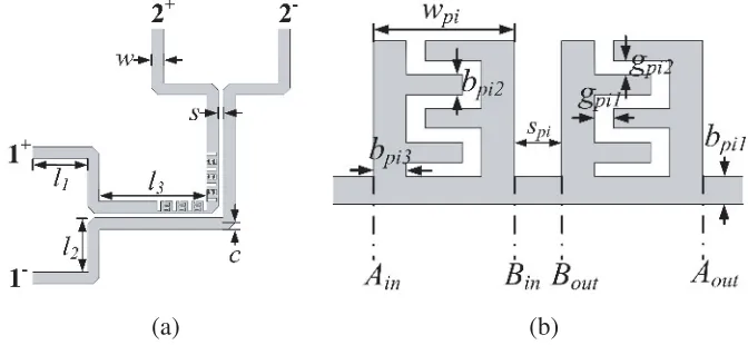
Figure 1 shows the schematic of the proposed compensated structure for the differential signals. Owing to the asymmetric structure at the corner of the bend differential signals, a phase imbalance is observed between the two differential lines. Periodic interdigital structures with large shunt capacitance are loaded on the inner line to compensate the phase difference of the bend discontinuous differential signals. Furthermore, the adjacent interdigital cells are connected by a narrow microstrip line, which can increase the inductance of the structure. Therefore, a hybrid inductance and capacitance compensation property is exhibited to suppress the common mode noise conversation of the bend differential pairs.
(a) (b)
Figure 1. The schematic of the proposed compensated structure: (a) bended differential pairs with periodic interdigital structure and (b) two adjacent interdigital cells connected with a narrow microstrip line.
From Fig. 1(a), the geometric parameters of the proposed compensate structure are described, where w is the width of the differential line, c the length of the chamfer of the differential line, and s the gap between the inner and outer lines. l1 and l2 are the lengths of input and output ports, andl3 is the length of the differential line. Fig. 1(b) shows the structure notations between the two adjacent interdigital cells. spi and bpi1 are the length and width of the narrow microstrip line, respectively. wpi is the width of the interdigital structure unit. bpi2 and bpi3 are the widths of the two coupling lines of the interdigital structure, respectively. gpi1 and gpi2 are the gap sizes of the interdigital structure at different positions, respectively.
Furthermore, in order to interpret the mechanism of the presented periodic interdigital structure in detail, a simplified equivalent circuit model between the two adjacent interdigital cells is built in Fig. 2. A hybrid inductance and capacitance characteristic is exhibited. Cp1 and L1 stand for the capacitance and inductance of the coplanar waveguide (CPW) in the interdigital structure, respectively. Cg is the coupling capacitance of the interdigital structures. Cp2 and L2 are the capacitance and inductance of the narrow microstrip line between the two adjacent interdigital capacitor.
The capacitanceCpi and inductance Li are calculated as [9]:
Cpi = εrε0
Si
h (1)
Li = liLpul (2)
where i is equal to 1 and 2, respectively. Si and li are the area and length of the microstrip line, respectively. εr and ε0 are the permittivity of the substrate and free space, respectively.
Lpul is the inductance of the CPW per unit length and can be calculated by:
Lpul=ZCWP√εeffc/c (3)
whereεeffc and Zcwp are the effective dielectric constant and impedance of the CPW, respectively. The gap capacitanceCg of the interdigital structure can be derived by:
Cg = 3ε0(1 +εr)bpi2
π cosh−1
2bpi2+gpi2
gpi2
+ ε0(1 +εr)
π
(bpi1+bpi2)
2 cosh
−1
b
pi1+bpi2+gpi2
gpi2
+4ε0(1 +εr)
π
(wpi−gpi1)
2 cosh −1 w pi gpi1 (4)
From above analysis, it can be observed that the internal coupling capacitance Cg of the periodic interdigital structure and the inductance L2 of the narrow microstrip line have a great effect on the compensation capacitance and inductance of the bend differential line.
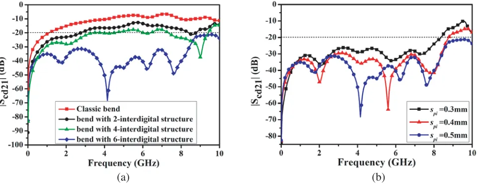
In order to evaluate the propagation characteristics of the proposed compensated structure for the differential signals, various EM computation methods are presented to calculate the scattering performances [10, 11]. As shown in Fig. 3(a), the influence of the number of the periodic interdigital cells on the differential to common mode conversion noise suppression performance is analyzed. With the increase of the number of the interdigital cells, the capacitance is enlarged to compensate the phase difference of the discontinuity of the bend differential lines. It is obviously found that the conversion noise can be prohibited greatly with increasing number of interdigital structures.
Furthermore, the inductance of the narrow microstrip line between the adjacent interdigital cells also has an effect on the differential to common mode conversion noise mitigation. From Fig. 3(b), the noise suppression depth becomes deeper with the increase of spi, which can increase the compensated inductance of the bend differential lines. By employing the periodic interdigital cells, a hybrid inductance and capacitance characteristic is introduced to compensate the phase imbalance of the bend discontinuity of the differential lines. The differential to common mode conversation noise is suppressed sufficiently.
(a) (b)
(a) (b)
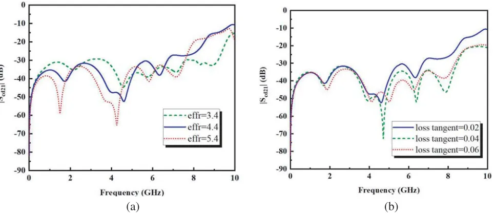
Figure 4. The effect of the frequency dependent parameters of the dielectric on the differential to common mode conversion noise mitigation: (a) the effective permittivity and (b) the loss tangent.
Moreover, the influences of the frequency dependent parameters of the dielectric on the scattering parameters of the proposed differential signal lines structure are analyzed. From Fig. 4(a), with decrease of the effective relativity of the substrate, the upper cutoff frequency of the differential-to-common mode noise conversion is increased, and the bandwidth is enlarged correspondingly. Furthermore, the loss tangent, one of the typical frequency depended parameters, also has a significant impact on the transmission performances. As can be seen from Fig. 4(b), if the loss tangent of the dielectric is increased, the attenuation level of the differential-to-common mode noise conversion at high frequency is steepened.
Based on the aforementioned analysis, the design procedure of the presented compensated structure can be summarized as follows: Firstly, the compensated capacitance and inductance can be calculated with the phase difference between the inner and outer lines at the bend discontinuity. Secondly, the number of the periodic interdigital cells can be determined with the noise suppression performance. Then, the initial parameters of the interdigital structure and the narrow microstrip line can be derived with the compensated capacitance and inductance. Finally, the specific sizes of the proposed structure is optimized with the EM simulator according to the designed predictions.
3. SIMULATION PREDICTION AND MEASUREMENTS
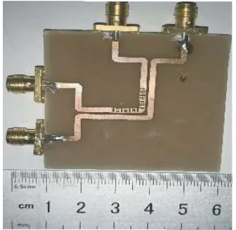
In order to verify the above analysis and design, a prototype circuit sample as shown in Fig. 5 is fabricated. The bend differential line is fabricated with the standard printed circuit board technique. FR-4 material with relative permittivity of εr = 4.4 and loss tangent of tanδ = 0.02 is employed as substrate. The thickness of the substrate and copper are h = 1.6 mm and t= 0.035 mm, respectively. By using full wave EM simulator Ansys HFSS, the final structure parameters are optimized as:
bpi1 = 0.15 mm, bpi2 = 0.212 mm, bpi3 = 0.5 mm, gpi1 = 0.2 mm, gpi2 = 0.15 mm, gpi3 = 0.8 mm,
w= 1.75 mm, s= 0.75 mm, spi= 0.5 mm, l1 = 8.25 mm, l2 = 10 mm,l3 = 16 mm, and c= 1 mm. The scattering properties of the proposed structure are measured by the VNA Keysight N5227B.
Figure 5. Photograph of the fabricated sample circuit.
Figure 6. Comparison between the proposed compensated structure and uncompensated struc-ture. (The simulated and measuredS-parameters denoted by (S.) and (M.), respectively.)
observed with the error in the manufacturing process and the welding of the SMA joint.
Furthermore, the differential-to-common-mode conversion results for different compensation structures of bend differential line are listed in Table 1 for comparison. It can be seen from the table that compared with the traditional compensated structure, good performances of wideband and steep suppression level are both observed with the proposed structure. Moreover, no additional area is required for the bend differential lines.
Table 1. Comparison with previous works using the compensation structure in internal line.
Size (λ0×λ0) Rejection level (dB) Rejection bandwidth (GHz) Occupy area
[4] N/A −20 DC-10 Occupy
[6] 0.5×0.5 −16.67 DC-6 Occupy
[7] N/A −15 DC-4 Occupy
Proposed 0.83×0.83 −20 DC-10 No occupy
λ0 is the wavelength at the center frequency of suppression bandwidth.
4. CONCLUSION
In this paper, a periodic interdigital structure is presented to suppress the differential to common mode conversion noise at the bend discontinuity of differential lines. An equivalent circuit model is built to explain the mechanism of the structure. In comparison with the uncompensated bend differential lines, a wideband and steep suppression of differential to common mode conversion noise is obtained with the proposed structure. Moreover, no additional occupying area is required for the bend differential line, which can be more useful for the multi-channel and miniaturized circuit system.
ACKNOWLEDGMENT
University under Grant K201901, and in part by the Major Project of Science and Technology of Anhui Province under Grant 18030901010.
REFERENCES
1. Fornberg, P. E., M. Kanda, C. Lasek, M. Piket-May, and S. H. Stephen, “The impact of a nonideal return path on differential signal integrity,” IEEE Trans. Electromagn. Compat., Vol. 44, No. 1, 11–15, Feb. 2002.
2. Guo, W.-D., G.-H. Shiue, C.-M. Lin, and R.-B. Wu, “Comparisons between serpentine and flat spiral delay lines on transient reflection/transmission waveforms and eye diagrams,” IEEE Trans. Microw. Theory Tech., Vol. 54, No. 4, 1379–1387, Apr. 2006.
3. Tsai, C.-H. and T.-L. Wu, “A broadband and miniaturized common-mode filter for gigahertz differential signals based on negative permittivity metamaterials,” IEEE Trans. Microw. Theory Tech., Vol. 58, No. 1, 195–202, Jan. 2010.
4. Wu, L.-S., J.-F. Mao, and W.-Y. Yin, “Slow-wave structure to suppress diffetential-to-common model conversion for bend discontinuity of differential signaling,” Proc. IEEE Elect. Design Adv. Packag. Syst. Symp., Hangzhou, China, Dec. 2011.
5. Lin, D.-B., “Signal integrity of bent differential transmission lines,”Electron. Lett., Vol. 40, No. 19, 1191–1192, Sep. 2004.
6. Chang, C.-H., R.-Y. Fang, and C.-L. Wang, “Bended differential transmission line using compensation inductance for common-mode noise suppression,” IEEE Trans. Compon. Packag. Manuf. Technol., Vol. 2, No. 9, 1518–1525, Sep. 2012.
7. Shiue, G.-H., W.-D. Guo, C.-M. Lin, and R.-B. Wu, “Noise reduction using compensation capacitance for bend discontinuities of differential transmission lines,”IEEE Trans. Adv. Packag., Vol. 29, No. 3, 560–569, 2006.
8. Ranade, S. R., R. K. Shevgaonkar, A. Sidhique, and P. H. Rao, “Mitigation of common mode noise in bent differential transmission line using curved PBG unit cell,” Microw. Opt. Technol. Lett., Vol. 60, No. 2, 347–352, 2018.
9. Zhu, H.-R., J.-J. Li, and J.-F. Mao, “Ultra-wideband suppression of SSN using localized topology with CSRRs and embedded capacitance in high-speed circuits,” IEEE Trans. on Microw. Theory and Tech., Vol. 61, No. 2, 764–772, 2013.
10. Duffy, A. P., A. J. M. Martin, A. Orlandi, G. Antonini, T. M. Benson, and M. S. Woolfson, “Feature selective salidation (FSV) for validation of computational electromagnetics (CEM). Part I — The FSV method,” IEEE Trans. Electromagn. Compat., Vol. 48, No. 3, 449–459, 2006.