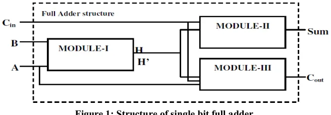
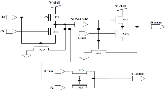
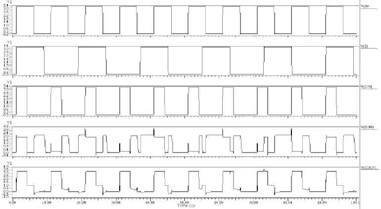
Implementation of Low Power Full Adder Using Semi XOR Semi XNOR on 120 nm Technology
Full text
Figure


Related documents
Study designs that permit analyzing continuous group data rather than discrete paired observations may provide an increased ability to discern interexaminer agreement, as does
In this section, the patients were asked questions related to the following: previous visits to the ED, difficulties encountered during the ED visit, satisfaction with the
In view of differential metabolic responses of various tissues under different stress conditions two important tissues of prawn such as muscle and hepatopancreas
As described above, situation awareness plays a significant role in the decision making process of emergency ambulance dispatchers.. Collectively, these observations present a number
A first step in that direction is to resolve the issue of optimal scheduling n jobs on a single resource of multiple availability, when the jobs are related by arbitrary
That is to say, if the two parents are random selections from the population, R (n,q,s’) may increase or decrease with increas- ing m (number of generations of intermating)
Seit Dagobert Freys Lemma zur Architekturzeichnung im Reallexikon der Kunst- geschichte haben die Funktionen der Zeichnung eine erste Definition gefunden.24 Sein Schema lotet,
