A Penta-Band Planar Inverted-F Antenna for Mobile Phone
Application Using LC-Tank-Stacked Network
Chao-Shun Yang*, Po-Chun Huang, and Christina F. Jou
Abstract—In this paper, a penta-band antenna design using matching network for mobile phone application is proposed. This design is composed of a planar inverted-F antenna (PIFA) and a LC-tank-stacked network. The LC-LC-tank-stacked network consists of two pairs of stacked chip-LC tank, which combine in parallel with the microstrip line feeding to the antenna. The PIFA can excite dual bands, and each pair of chipLC tanks can effectively widen the lower and upper bandwidth, respectively. According to measured results, the bandwidth can cover 824–960 MHz/1710–2170 MHz band for WWAN application (VSWR = 3 : 1). The peak antenna gain is better than 0.5 dBi and 3.4 dBi for lower and upper operating band, respectively. And the measured radiation efficiency is about 40–60% and 40–70% for lower and upper operating band, respectively.
1. INTRODUCTION
Recently, the rapid progress of wireless communication technologies increases the difficulty of dual-band antenna design toward compact, slim profile and broadband for portable devices. In order to achieve dual-broad bands, some designs have been proposed such as active components (pin diode or varactor) to switch or tune the frequency configuration or the passive chip components (inductor or capacitor) called matching network to match the bandwidth. Therefore, there are some designs such as a dual-feed switching L-shaped or triangular radiator fed by pi-shaped matching network to cover different bands [1, 2], loop radiator shorting to ground plane fed by chip-LC-tank series matching network to cover two operating bands [3], two-path radiator and a strip protruded from ground fed by chip-LC-tank band-stop matching network to cover dual bands [4], slotted radiator fed by chip-LC band-stop matching network to cover dual bands [5], loop radiator with an inductively branch strip to cover two operating bands [6], and stacked inverted-F antenna with parallel chip-LC-tank matching network to cover dual bands [7]. Here, an antenna design fed by a particular LC-tank-stacked matching network is presented. The antenna is a PIFA without clearance region that can produce the dual bands. However, the LC-tank-stacked matching network consisting of two pairs of chip-LC tanks can add the parasitic mode close to original lower band and upper band, respectively. Especially, one pair of chip-LC tanks near the feeding microstrip line can widen the lower band, and the other pair of chip-LC tanks near the ground plane can widen the upper band. Hence, the proposed antenna can achieve the desired dual operating bands 824–960 MHz/1710–2170 MHz for WWAN application (VSWR = 3 : 1). Moreover, the PIFA lower/upper bandwidth can be improved by the LC-tank-stacked matching network form 10%/13% to 17%/26% to cover the WWAN operating band 15%/23%.
2. ANTENNA CONFIGURATION AND DESIGN
The proposed antenna configuration is composed of a PIFA for producing dual bands and a LC-tank-stacked network for dual-band bandwidth enhancement. Figure 1 shows the complete structure. The
Received 28 October 2014, Accepted 17 November 2014, Scheduled 23 November 2014
* Corresponding author: Chao-Shun Yang ([email protected]).
Figure 1. The implement of the proposed antenna.
Simulated L =26.5 mm L =28.5 mm L =30.5 mm
Simulated L =5 mm L =9 mm L =13 mm fi x
"
500 1000 1500 2000 2500
-30 -24 -18 -12 -6 0
Return Loss (dB)
Frequency (MHz)
500 1000 1500 2000 2500
-30 -24 -18 -12 -6 0
Return Loss (dB)
Frequency (MHz) 2
2
2 1
1
1
(a)
(b) (c)
(d) (e)
Figure 2. (a) Proposed antenna dimension and structural parameters denotation. (b) The simulated return loss as a function of L1. (c) The simulated return loss as a function of L2. (d) The antenna
500 1000 1500 2000 2500 -30
-24 -18 -12 -6 0
1160 MHz Simulated
The proposed PIFA Conventional PIFA
Return Loss (dB)
Frequency (MHz) 880 MHz
1950 MHz
(a) (b)
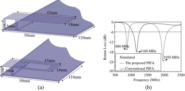
Figure 3. Comparison between proposed PIFA and conventional PIFA. (a) Top for conventional PIFA
and bottom for proposed PIFA. (b) The simulated return-loss result.
500 1000 1500 2000 2500
PIFA without LC-tank-stacked network PIFA with LC-tank-stacked network
Return Loss (dB)
Frequency (MHz)
820 MHz 960 MHz1710 MHz 2170 MHz
" (a) (b)
-30 -24 -18 -12 -6 0
Figure 4. (a) The implement of the proposed antenna with LC-tank-stacked network. (b) The
simulated return loss of PIFA and PIFA with network.
500 1000 1500 2000 2500 BW=13% BW=10%
2100 MHz 1845 MHz
925 MHz
Frequency (MHz) 835MHz
500 1000 1500 2000 2500
Zin=57+j0
@1950 MHz
Input Impedance (ohms) Resistance
Reactance
Frequency (MHz)
Zin=42+j0@880 MHz
-1000 -750 -500 -250 0 250 500 750 1000
-30 -24 -18 -12 -6 0
Return Loss (dB)
500 1000 1500 2000 2500 -1000 -750 -500 -250 0 250 500 750 1000
Zin=13+j0
@2 240MHz
Zin=123+j0
@1960 MHz
Input Impedance (ohms)
Frequency (MHz) Resistance
Reactance
Zin=21+j0@1730MHz
500 1000 1500 2000 2500
-1000 -750 -500 -250 0 250 500 750 1000
Zin=15+j0
@2200 MHz
Zin=149+j0
@1910 MHz
Zin=36+j0@1760 MHz Zin=24+j0
@960 MHz
Zin=42+j0
@940MHz
Input Impedance (ohms)
Frequency (MHz) Resistance Reactance
Zin=45+j0
@850 MHz
500 1000 1500 2000 2500
-400 -300 -200 -100 0 100 200 300 400
Z in =84+j0@950 MHz
Input Impedance (ohms)
Frequency (MHz) Resistance Reactance
Z in =40+j0@860 MHz
(c) (d) (e) (f) (g) (h) 0 -6 -12 -18 -24 -30
Return Loss (dB)
500 1000 1500 2000 2500
Frequency (MHz) 0 -6 -12 -18 -24 -30
Return Loss (dB)
500 1000 1500 2000 2500
Frequency (MHz) 0 -6 -12 -18 -24 -30
Return Loss (dB)
500 1000 1500 2000 2500
Frequency (MHz)
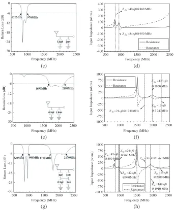
Figure 5. (a) The simulated return loss result of the PIFA. (b) The simulated input impedance result of the PIFA. (c) The simulated return loss result of the PIFA with chip-LC tank for lower band. (d) The simulated input impedance result of the PIFA with chip-LC tank for lower band. (e) The simulated return loss result of the PIFA with chip-LC tank for upper band. (f) The simulated input impedance result of the PIFA with chip-LC tank for upper band. (g) The simulated return loss result of the PIFA with LC-tank-stacked network for dual-band matching. (h) The simulated input impedance result of the PIFA with LC-tank-stacked network for dual-band matching.
ground-plane size is 50×110×0.8 mm3 using a FR4 substrate with relative permittivity 4.4, and the PIFA size is 42×18×7.5 mm3using metal injection molding. The PIFA consists of a long strip and short ladder-shape strip. The structural parameterL1 can be used to define the long-strip length, andL2 can
be used to define short ladder-shaped strip length as shown in Figure 2(a). Note that the structural
parameters L1 and L2 can control the dual-band ratio. L1 can manipulate the dual-band movement
until the lower band arrives at 880 MHz as shown in Figure 2(b), and then L2 can fix lower band at
880 MHz and manipulate the upper band arriving at 1950 MHz as shown in Figure 2(c). Figures 2(d), (e) show the current distribution at lower-band 880 MHz and at upper-band 1950 MHz. It can be observed thatL1 and L2 can affect the dual bands. However,L2 length is not sensitive to affect the lower band
dual bands and reduce the dual bands toward lower frequency compared to the conventional PIFA [8]. Fig. 3(a) shows the conventional PIFA (an entire metal patch) and the proposed PIFA with the same size. Note that Fig. 3(b) shows the simulated return-loss result between conventional PIFA and the proposed PIFA which can explain the lower dual resonances.
PIFA can provide the mechanism of dual-band ratio; however, the LC-tank-stacked network can widen the dual-band bandwidth to cover the WWAN operating band for the 3 : 1 VSWR. As shown in Figure 4(a), the pair of chip-LC tanks near the microstrip line can widen the lower band withC1= 6 pF
and L1 = 3 nH, and the other pair of chip-LC tanks can widen the upper band with C2 = 0.9 pF and
L2 = 2 nH. Figure 4(b) shows the return loss of PIFA and PIFA with LC-tank-stacked network. It is
obvious that the LC-tank-stacked network can add parasitic mode at lower and upper bands to achieve WWAN operating band. The dual-broad bands can be explained by input impedance as shown in Figure 5.
Figures 5(a), (b) show the simulated return loss and input impedance results of PIFA, and the resonant frequency at 880 MHz/1950 MHz can be observed at lower and upper bands, respectively.
When one pair of chip-LC tanks (L = 2 nH and C = 7.6 pF) combines in parallel with microstrip
line feeding to the PIFA, there are two resonances at 860 MHz/950 MHz to widen the lower band
as shown in Figures 5(c), (d). Similarly, the other pair of chip-LC tanks (L = 1.8 nH and C =
0.9 pF) combines in parallel with microstrip line feeding to the PIFA. There are three resonances at
500 1000 1500 2000 2500
BW=26% 965 MHz
Frequency (MHz) 810 MHz
2195 MHz 1690 MHz
BW=17%
Measured Simulated (HFSS) -30
-24 -18 -12 -6 0
Return Loss (dB)
Figure 6. The simulated and measured return loss result of the proposed antenna.
Theta
Response (dB)
-35 5
-30 -25 -20 -15 -10 -5 0 Z
Y X
Azimuth = 100.0 Elevation = -30.0 Roll = -70.0
Phi
Response (dB)
-35 5
-30 -25 -20 -15 -10 -5 0 Z
Y X
Azimuth = 100.0 Elevation = -30.0 Roll = -70.0
(a)
Theta Re s pons e (d B ) -35 5 -30 -25 -20 -15 -10 -5 0 Z Y X
Azimuth = 100.0 Elevation = -30.0 Roll = -70.0
Response (dB)
-35 5 -30 -25 -20 -15 -10 -5 0 Z Y X
Azimuth = 100.0 Elevation = -30.0 Roll = -70.0
Total Gain (dBi) -35 5 -30 -25 -20 -15 -10 -5 0 Z Y X
Azimuth = 100.0 Elevation = -30.0 Roll = -70.0
Total Gain (dBi) -35 5 -30 -25 -20 -15 -10 -5 0 Z Y X
Azimuth = 100.0 Elevation = -30.0 Roll = -70.0
(d) (e)
(f) (g)
Figure 7. The measured 3-D radiation pattern. (a) The antenna measurement coordination. (b) E
-theta polarization at 900 MHz. (c) E-phi polarization at 900 MHz. (d) E-theta polarization at
1900 MHz. (e)E-phi polarization at 1900 MHz. (f) Total gain at 900 MHz. (g) Total gain at 1900 MHz.
800 900 1000 1600 1800 2000 2200 0 20 40 60 80 100 Gain (Measured)
Radiation Efficiency (%)
Frequency (MHz) Efficiency (Measured) -2 -1 0 1 2 3 4 5 6
Antenna Gain (dBi)
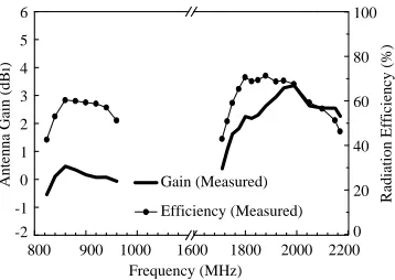
Figure 8. Measured results of the antenna peak gain and the antenna radiation efficiency.
3. MEASUREMENT ANTENNA RADIATION CHARACTERISTICS
For the antenna radiation pattern, the measured radiation pattern is shown in Figure 7. The coordinate
definition is shown in Figure 7(a). Figures 7(b), (c) show the radiation pattern of the E-theta
polarization and E-phi polarization at 900 MHz, respectively. Figures 7(d), (e) show the radiation
pattern of the E-theta polarization and E-phi polarization at 1900 MHz, respectively. Note that the total gain is mainly distributed onxy-plane at 900 MHz and at 1900 MHz as shown in Figures 7(f), (g). The measured antenna gain and radiation efficiency are shown in Figure 8. For the low band, the peak antenna gain is 0.4 dBi, and the efficiency is between 40–60%. For the upper band, the peak gain is 3.4 dBi, and the efficiency is between 40–70%.
4. CONCLUSION
In this paper, a penta-band antenna design has been proposed. This design is composed of PIFA and a LC-tank-stacked network. By using the LC-tank-stacked network, the dual-broad bands are achieved
effectively. According to measured results, the lower-/upperband can cover 824–960 MHz/1710–
2170 MHz for WWAN application (VSWR = 3 : 1). The peak antenna gain is 0.5 dBi and 3.4 dBi for lower and upper bands, respectively. And the measured antenna radiation efficiency is between 40–60% and 40–70% for lower and upper bands, respectively.
REFERENCES
1. Lin, P.-W. and K.-L. Wong, “Dual-feed small-size LTE/WWAN strip monopole antenna for tablet computer applications,”Microwave Opt. Technol. Lett., Vol. 55, No. 11, 2571–2576, Nov. 2013. 2. Hsieh, Y.-T., K.-L. Wong, Y.-T. Liu, and H.-T. Chen, “Printed dual-feed triangular patch antenna
disposed in a small notch in the handheld device system ground plane for LTE/WWAN operation,” Microwave Opt. Technol. Lett., Vol. 55, No. 11, Nov. 2013.
3. Chu, F.-H., Y.-C. Kao, and K.-L. Wong, “Penta-band WWAN handset antenna embedded in a small notch in the system ground plane,”AP-S Int. Symp., 1–2, Jul. 8–14, 2012.
4. Lin, P.-W. and K.-L. Wong, “Internal WWAN handset antenna formed by a monopole strip radiator and a clearance region thereof as monopole slot radiator,”Proc. Antennas and Propagat. Int. Symp., 1361–1364, Oct. 29–Nov. 2, 2012.
5. Lin, P. W. and K. L. Wong, “Simple monopole slot antenna for WWAN/LTE handset application,” Asia-Pacific Microw. Conf. Proc., 829–832, 2011.
6. Wong, K. L. and M. T. Chen, “Small-size LTE/WWAN printed loop antenna with an inductively
coupled branch strip for bandwidth enhancement in the tablet computer,”IEEE Trans. Antennas
Propag., Vol. 61, No. 12, 6144–6151, Dec. 2013.
7. Wong, K.-L. and C.-Y. Tsai, “Small-size stacked inverted-F antenna with two hybrid shorting
strips for LTE/WWAN tablet device,” IEEE Trans. Antennas Propag., Vol. 62, No. 8, 3962–3969,
May 2014.
8. Taga, T. and K. Tsunekawa, “Performance analysis of a built-in planar inverted F antenna for