Eman G. Ouf1, 3, *, Esmat A. F. Abdallah1, Ashraf S. Mohra2, and Hadia M. S. Elhennawy3
Abstract—In this paper, an electronically switchable ultra-wideband (UWB)/dual-band bandpass filter using defected ground structures (DGSs) is proposed. The proposed filter consists of meandered inter-digital coupled line sections, stepped impedance open stubs, coupled lines, and rectangular DGSs to realize high performance in the operation band with a compact size of 12.5 mm ×10 mm. The proposed filter is designed on an RT/Teflon substrate (εr= 2.2, h= 0.7874 mm). The main advantage of the proposed filter is the reconfiguration of ultra-wide bandpass filter to dual-band bandpass filter. UWB has passband from 3.6 GHz to 10.6 GHz with upper wide stopband attenuation better than 20 dB up to 18 GHz. The dual passbands extend from 3.8 GHz to 5 GHz and from 9.5 GHz to 10.8 GHz. This filter is able to provide interference immunity from unwanted radio signals, such as wireless local area networks (WLAN), worldwide interoperability for microwave access (WIMAX) that cohabit within the UWB spectrum and X (Military) band of satellite from 7 GHz to 8 GHz. The state of filter can be changed by using switching matrix equipment (mini circuit, replacement of PIN diodes). To validate the design theory, an electronically switchable UWB/dual-band bandpass filter using DGSs is designed, fabricated, and measured. Good agreement is found between simulated and measured results.
1. INTRODUCTION
Ultra-Wideband (UWB) systems have attracted increasing attention since the Federal Communications Commission (FCC) released the unlicensed use of frequency spectrum 3.1–10.6 GHz for UWB applications in 2002 [1]. Since then, UWB technology has been developed clearly, and many structures of wide-band filters have been designed. Due to the interference from the undesired Wireless Local Area Network (WLAN) signal (2.4, 3.6, 4.9, 5, 5.9 GHz) and satellite communication signals (7/8 GHz) with the UWB system, a UWB BPF with notch bands is necessary to avoid this interference signal. On the other hand, a dual-band BPF can be designed to operate in bands far from one or more of these undesired signals.
Due to an increasing demand of dual-band microwave devices, much research has been done. The direct method to design a dual-band bandpass filter consists of two independently bandpass filters [2]. Weng et al. [3] pointed out that this approach requires a larger circuit size and needs extra impedance matching networks for diplexer-like structure. Another method of designing a dual-band bandpass filter is to use a cascade connection of a BPF and a bandstop filter [4]. A dual-band bandpass filter (BPF) is also achieved through a cascade connection of open- or short-circuited stub structures [5, 6]. All these designs need a large circuit size.
During the last decade, patterned ground structures, which have also been referred as ‘defected’ or ‘slotted’ ground structures have been investigated. Recently, a slotted ground structure can be made
Received 7 January 2019, Accepted 1 March 2019, Scheduled 20 March 2019
* Corresponding author: Eman Gamal Ouf ([email protected]).
1 Electronics Research Institute, Dokki, Giza, Egypt. 2 Benha Faculty of Engineering, Benha University, Benha, Egypt. 3Faculty
more compact by extending the coupling gap; as a result the coupling capacitance increases. Slotted ground structures have been applied to various applications such as spurious-suppression of lowpass filters [7]. In general, slotted ground structure shows advantages including an efficient and flexible usage of the ground plane, compactness, and wide-band operation. Broadband feature is particularly attractive for applications in high data-rate communication systems.
In [8], Shan et al. proposed a UWB filter with a notch at 6 GHz. However, in some applications, it is not applicable to use such a filter with small notch bandwidth. Dual bands of operation become more suitable to overcome the problem of interference at multiple bands. So in this paper, we present an electronically switchable UWB/dual band bandpass filter, which has two passbands far from WLAN signal, WiMAX, and satellite communication signals; therefore, there is no interference.
The paper is organized as follows. Section 2 introduces the design of the proposed filter in terms of the shape of the filter, its dimensions, and the simulation results. Section 3 introduces the equivalent lumped circuit model of the proposed design while Section 4 provides the analysis of the proposed filter. Section 5 introduces the fabrication and measurement of the proposed filters together with simulated results. The conclusion is given in Section 6.
2. FILTER DESIGN
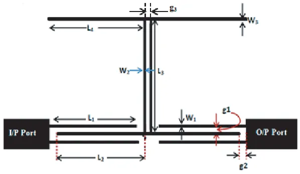
The idea of using Multimode resonator (MMR) technique is originally discussed in [8]. However, the UWB performance is not preferred in some applications. Dual bands of operation are mandatory in many applications that require band separation. The proposed design in this paper employs the dual-band principle. The proposed filter consists of parallel coupled lines section and H-shaped section as shown in Figure 1. The proposed filter is designed on a Rogers RT5880 substrate of relative permittivity 2.2, height 0.7874 mm, and tanδ = 0.0009. The dimensions of the proposed design are obtained using extensive parametrical studies and Particle Swarm Optimization Algorithm done on CST MWS version 2016. All dimensions are as follows: L1 = 7.75 mm, L2 = 7.85 mm, L3 = 8.6 mm, L4 = 7.7 mm,
W1 = 0.2 mm, W2 = 0.15 mm, W3 = 0.2 mm, g1 = 0.2 mm, g2 = 0.25 mm, g3 = 0.2 mm. The overall
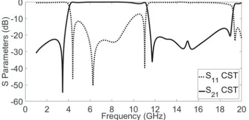
dimension of the proposed filter is 16.5 mm×9.4 mm. Figure 2 shows the simulated S parameters of the proposed filter by using CST MWS.
In order to reduce the filter size, three steps are employed. The first one is converting the interdigital coupled lines structure into meander lines as shown in Figure 3. We modified and optimized its meandering, thereby obtaining the desired characteristics of ultra-wideband. Figure 4 demonstrates the simulated results of the proposed filter with meandering of interdigital coupled line. It should be noticed that matching in the filter shown in Figure 1 is better than that shown in Figure 3 with meandering.
The second step is converting the open circuit stub to a stepped impedance open stub as illustrated
Figure 2. The simulatedS11 and S21 using CST software package.
Figure 3. The proposed filter with meander interdigital coupled lines.
Figure 4. The simulated results of the proposed filter with meander interdigital coupled lines.
Figure 5. The proposed filter with meandering and stepped impedance open stub.
Figure 6. The simulated results of the proposed filter with meandering and stepped impedance open stub.
Figure 7. The proposed filter with meandering, stepped impedance open stub and DGS.
Figure 8. The simulated results of the proposed filter with meandering, stepped impedance open stub and DGS.
3 dB bandwidth extends from 3.6 GHz to 10.5 GHz. As the reflection coefficient |S11|around 5 GHz is
not good, the third modification step is proposed.
The third step is adding a defected ground structure (DGS) under the input and output ports of the proposed filter as indicated in Figure 7. This procedure improves the reflection coefficient performance of the proposed filter and adding two resonances at 7.5 GHz and 9.6 GHz. The improved S11 and S21
after the last modification are presented in Figure 8. All dimensions of the proposed filter are as follows:
L1 = 3.75 mm, L2 = 1.95 mm, L3 = 1.8 mm, L4 = 7.5 mm, L5 = 2.1 mm, L6 = 1 mm, L7 = 5.65 mm,
W1 = 0.2 mm,W2 = 0.5 mm, W3 = 0.15 mm, g1 = 0.2 mm, g2 = 0.2 mm, g3 = 0.3 mm. The simulated
Figure 9. The structure of the proposed filter.
Next, we think about how to make the proposed filter tunable from UWB BPF to dual bands. This can be obtained by connecting the two coupled stubs in the middle of the filter by PIN diodes as shown in Figure 9. The design procedure of this filter depends on the connection between two coupled stubs; this connection is controlled by using switching matrix equipment (mini circuit) [16] instead of PIN diodes where the character D refers to the diode, and the different diodes states will be described as follows:
(i) WhenD1 andD2 are ON, the two parts of the filter are connected, and a UWB BPF from 3.6 GHz
up to 10.5 GHz occurs.
(ii) WhenD1 and D2 are OFF, the two parts of the filter are disconnected, and a dual-band BPF with
passbands from 3.8 GHz to 5 GHz and from 9 GHz to 10.8 GHz occurs.
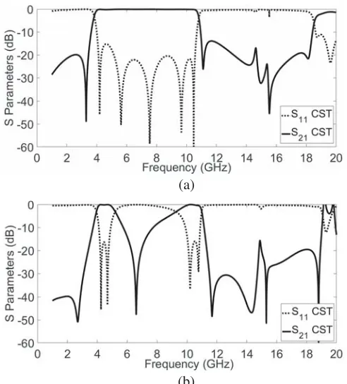
Figure 10 shows S parameters of the proposed filter with different states of diode by using CST MWS version 2016. Figure 10(a) shows the simulatedS11 and S21 for ON state, which is a UWB BPF
from 3.6 GHz to 10.5 GHz. Figure 10(b) shows the simulatedS11 andS21for OFF state, which is a dual
band BPF and can be tuned from 3.8 GHz to 5 GHz and from 9 GHz to 10.8 GHz. Thus, we avoided unwanted interference such as WLAN (IEEE 802.11p- 2010) which is intended for use in vehicular communication systems with band of 5.9 GHz (5.850–5.925 GHz) and may cause unwanted interference with UWB, WLAN (IEEE 802.11a), WIMAX (in Europe IEEE802.16), United States FCC-U-NIII-2C (5.690- 5.710 GHz), and FCC-U-NIII-3 (5.690–5.730 GHz), and the FCC further clarified the use of channels in the 5.470–5.725 GHz band to avoid interference with weather radar systems (TDWR), WLAN, United States FCC-U-NIII-2C (5.490–5.510 GHz), and WIMAX at 5.5 GHz, in addition to avoiding interference with X (Military) band of satellite from 7 GHz to 8 GHz.
From Figure 10(b), it is noticed that the out of band rejection around 8.5 GHz is not acceptable. So a new modification is required to improve it. An open circuit stub with lengthL8= 6.8 mm is added as
shown in Figure 11. The length of this stub isλg/4 whereλg is the guide wavelength atfc= 7.05 GHz. The design procedure of the modified filter depends on the connection between the two coupled stubs in the middle of the shape and connection with open circuit stub L8; these connections are
controlled by using switching matrix equipment (mini circuit) instead of PIN diodes where character D refers to the diode, and different diodes states will be described as follows:
a. When D1 and D2 are ON, andD3 is OFF, the two parts of the filter are connected, and a UWB
BPF from 3.6 GHz to 10.5 GHz occurs.
b. WhenD1 and D2 are OFF, and D3 is ON, the two parts of the filter are disconnected, and a dual
(a)
(b)
Figure 10. The simulated S11 and S21 using CST software package for different diode states. (a) D1
and D2 ON state, (b)D1 and D2 OFF state.
L8
D1
D2
D3
Figure 11. The structure of the proposed filter with open circuit stub.
Figure 12 shows the simulated results of the modified filter design. It should be noticed that the out of band rejection around 8.5 GHz is improved compared to before (S21 is improved by more than
(a)
(b)
Figure 12. The simulatedS11andS21 using CST software package for different diode states with open
circuit stub. (a)D1,D2 ON state andD3 OFF state, (b) D1, D2 OFF state andD3 ON state.
3. THE EQUIVALENT LUMPED CIRCUIT MODEL ANALYSIS OF THE PROPOSED DESIGN
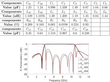
Figure 13 shows the equivalent lumped circuit model of the proposed UWB BPF that is shown in Figure 7. The equivalent lumped circuit model results are obtained using circuit model tool of the Advanced Design System (ADS) 2017. The lumped element values are manually optimized by changing each element value so that it can have good agreement with the simulated results obtained from the full wave simulator.
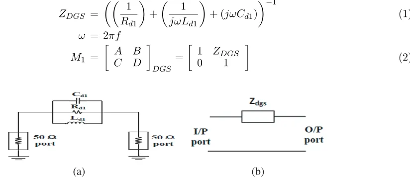
The whole equivalent circuit of the proposed filter can be divided into the following subsections: DGS part at input and output ports, interdigital coupled lines and stepped impedance open stub. As shown in the lumped element model (Figure 13) Rd1, Cd1, Ld1, Rd2, Cd2, and Ld2 represent the
equivalent resistance, inductance, and capacitance of the defected ground structure (DGS) [11]. L5,C5,
L6, and C6 represent the equivalent inductance and capacitance of the stepped impedance resonator
(SIR). Interdigital coupled arm is represented by the series capacitance with parasitic inductance and resistance, and shunt capacitances [12] as shown in Figure 13.
The various components values of the equivalent lumped circuit model shown in Figure 13 are listed in Table 1. The comparative S-parameters versus frequency response of EM simulation and circuit model are illustrated in Figure 14. One can notice that there is a very good agreement between the simulated and equivalent lumped circuit model results.
Table 1. Components’ values of the equivalent lumped circuit model shown in Figure 13.
Components Cd1 Cd2 C1 C2 C3 C4 C5 C6
Value (pF) 1.25 1.24 0.996 1.339 1.49 0.87 1.04 0.66
Components Ld1 Ld2 L1 L2 L3 L4 L5 L6
Value (nH) 1.109 1.1076 1.39 1.208 1.19 1.45 0.84 1.44
components Rd1 Rd2 R1 R2 R3 R4
Value (Ω) 0.269 0.163 0.001 0.0198 0.224 0.93
components Cs1 Cs2 Cs3 Cs4 Cs5 Cs6
Value (pF) 0.25 0.61 1.518 0.967 0.6 0.238
Figure 14. The results of equivalent circuit model and EM simulation of the proposed filter shown in Figure 7.
4. ANALYSIS OF THE PROPOSED FILTER
The proposed filter, Figure 7, consists of inter-digital coupled line sections, stepped impedance stubs, coupled lines, and rectangular DGS. The first section consists of DGS at the input and output parts as shown in Figure 7. This DGS part consists of R,L, and C circuit as shown in Figure 13 namely Rd1,
Cd1, and Ld1 from the input side andRd2, Cd2,Ld2 from the output side. The second section is
(a) (b)
Figure 15. (a) RLC equivalent circuit for unit DGS and (b) the equivalent transmission line network of the DGS part.
4.2. The Second Section
The input/output section consists of two coupled lines with high impedance line as shown in Figure 16(a), while the equivalent transmission line network is shown in Figure 16(b).
50
Ω
50
Ω
(a) (b)
Figure 16. (a) Schematic and (b) equivalent transmission line network of the inter-digital coupled lines [13].
TheABCD matrix for the coupled line can be expressed as [9]:
MC = ⎡ ⎢ ⎢ ⎣
Zoe+Zo0
Zoe−Zo0
cosθ1 −j 2
4ZoeZoo
Zoe−Zo0
cos2θ1
sinθ1 −(Zoe−Zo0) sinθ1
j 2 Zoe−Zo0
sinθ1 Zoe+Zo0
Zoe−Zo0
cosθ1
⎤ ⎥ ⎥
⎦ (3)
Zo and θ1 represent the characteristic impedance and electrical length of the coupled line, respectively,
while J is the admittance inverter. The admittance inverter J inABCD matrixMc can be replaced by the even and odd mode characteristic impedances (Zoe & Zoo) of the coupled line [9]:
Each of Zoe and Zoo can be calculated using equations in [10]:
TheABCD matrix of the high impedance line can be expressed as [9]:
MH = ⎡
⎣ jcosβHlH jZHsinβHlH
ZH
sinβHlH cosβHlH ⎤
where ZH is the high impedance line, βH the propagation constant, and lH the length of the high impedance line.
From Equations (3)–(4), theABCD matrix of the second part of the proposed filter is:
M2 =
A B C D
second section
=MC×MH (5)
4.3. The Third Section
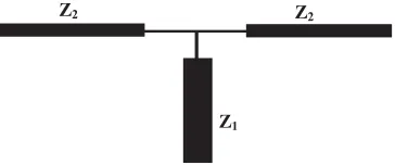
The middle section of the proposed filter consists of a T-shaped resonator as in Figure 17.
Z1
Z2 Z2
Figure 17. T-shape equivalent.
From Figure 17, it is clear that impedance Z2 is parallel with another Z2, and both are in series
withZ1, then:
Zt=Z1+
Z2
2 (6)
Then, the T-shape section becomes an open circuit stub (O.C), and the ABCD matrix of the middle part can be expressed as follows [9]:
M3=
A B C D third section = 1 0 j Zt
tanβtlt 1
(7)
The characteristic impedance and propagation constant of each section can be calculated as in [10]. Therefore, from Equations (2), (5), and (7), it is clear that the totalABCDmatrix of the proposed filter can be expressed as:
A B C D
total
=M1×M2×M3×M2×M1 (8)
The equations for computing the reflection and transmission coefficients from the previous set ofABCD -parameter values of the proposed filter can be written as follows [9]:
S11 =
A+ B
Z0 −
cZ0−D
A+ B
Z0
+cZ0+D
(9)
S21 =
2
A+ B
Z0
+cZ0+D
(10)
The return loss (RL) and insertion loss (IL) of the proposed filter are defined by the following equations:
RL(dB) = 20 log|S11| (11)
IL(dB) = 20 log|S21| (12)
Figure 18 shows the numerical results by using Mat-lab program version 2016 and simulated results by using CST MWS version 2016 of the proposed filter. Regarding S11, there is frequency shift between
Figure 18. The numerical analysis and simulated results of the proposed filter shown in Figure 7.
above 10.5 GHz between the numerical and simulated results, which may be attributed to the different methods of analysis used in the CST and Mat-lab program. Finally, from Figure 18, one can observe that the two results are in good agreement.
The proposed filter is compared with similar filters as given in Table 2. It is noticed that the proposed filter is distinguished from other published filters due to smaller size. The proposed design achieves total area reduction of more than 30% compared with [8], 51% compared with [14], and 60% compared with [15].
Table 2. Comparison of the proposed filter with published UWB Bandpass filters.
Ref. Dielectric constant
(εr)
Height
(mm) Size of filter
Minimum & Maximum values of S parameters in pass band (GHz)
Passband (GHz)
Impedance matching
(dB) S11(dB) S21(dB)
Ref. [8] 3.38 0.508 12 mm×15 mm −3 to−60 −0.1 to−3 3.6–10.1 <−15
Ref. [14] 4.4 1.6 20 mm×13 mm −3 to−23 −1.5 to−3 2.78–10.95 <−14
Ref. [15] 2.2 1 32 mm×10 mm −3 to−55 −0.1 to−3 2.6–10.6 <−17
Our work 2.2 0.7874 12.5 mm×10 mm −3 to−58 −0.1 to−3 3.8–10.8 <−17
5. FABRICATION AND MEASUREMENTS
The designed filters are fabricated using thin film technology and photolithographic technique on a Rogers RT 5880 (lossy) substrate with (εr = 2.2, h = 0.7874 mm, and tanδ = 0.0009). Photos of the fabricated filter are shown in Figure 19. The connecting wires are soldered to the circuit, then connecting the diode switch matrix tool (that replaces the PIN diode switch). The filters are measured using the vector network analyzer (N9928A FieldFox Handheld Microwave Vector Network Analyzer, 26.5 GHz).
(a)
(b)
Figure 20. The simulated and measured S11 and S21 without O.C stub. (a) D1 and D2 ON state
(with frequency range from 1 GHz to 20 GHz) and (b)D1 and D2 OFF state.
Figure 20(a) shows the measured and simulated results of the proposed filter at ON state with frequency range from 1 GHz to 20 GHz. It should be noted that the frequency range is extended up to 20 GHz in order to show that the out of band rejection is good, and the measured 3 dB passband of the proposed filter is between 3.6 and 10.6 GHz. Figure 20(b) shows the measured and simulated results of the proposed filter at OFF state, and the dual bands with 3 dB passbands extend from 3.8 GHz to 5 GHz and from 9 GHz to 10.8 GHz.
Photos for the fabricated filter with open stub are shown in Figure 21. Figure 22(a) shows the measured and simulated results of the proposed filter with open stub at D1,D2 ON state andD3 OFF
with frequency range from 1 GHz to 20 GHz. It should be noted that the out of band rejection is good, and the measured 3 dB passband of the proposed filter is between 3.6 and 10.6 GHz. Figure 22(b) shows the measured and simulated results of the proposed filter with open stub at D1, D2 OFF state and
D3 ON, and the dual bands with 3 dB passbands extend from 3.8 GHz to 5 GHz and from 9.5 GHz to
10.8 GH.
(a)
(b)
Figure 22. The simulated and measured S11 and S21 with O.C stub. (a) D1, D2 ON and D3 OFF,
(b)D1,D2 OFF andD3 ON.
6. CONCLUSION
An Electronically Switchable Ultra-Wide Band /Dual-band Bandpass Filter using DGS has been designed, simulated, and fabricated. Introducing DGS at input and output ports of the proposed filter produces two resonances at 7.5 GHz and 9.6 GHz and improves the performance of proposed filter, while an overall size reduction of 20% is obtained. The meander lines and stepped impedance open stub are also used to reduce the overall size. By adjusting the connection between the coupled lines in the center of the design, the center frequency and 3 dB frequency band can be easily adjusted. The proposed filter achieves UWB performance with good selectivity and low insertion loss in the passband from 3.6 to 10.5 GHz and good stopband from 10.6 to 18 GHz. Moreover, it achieves dual bands with good stopband from 5 GHz to 9.5 GHz and from 10.8 GHz to 18 GHz by using open circuit stub to suppress unwanted interference signals in the band of WLAN WIMAX, and X (Military) band of satellite. Two packages of software were used, namely CSTMWS 2016 and Advanced Design System (ADS) 2017 to design and simulate the filters. In addition, the model analysis of the proposed filter is carried out using Matlab 2016. The measured, Matlab analytical, and CSTMWS simulated results of the proposed filter show very good agreement. The overall size of the filter is 12.5 mm×10 mm, which is suitable to be integrated in the modern ultra-wideband wireless communication systems.
REFERENCES
1. Federal Communications Commission (FCC), Revision of Part 15 of the Commissions Rules Regarding, “Ultra-wideband transmission systems,” First Report and order, FCC 2–48, Apr. 22, 2002.
3. Weng, M.-H., H.-W. Wu, and Y.-K. Su, “Compact and low loss dual-band bandpass filter using pseudo-interdigital stepped impedance resonators for WLANs,” IEEE Microwave Wireless Component Letters, Vol. 17, No. 3, 187–189, Mar. 2007.
4. Tsai, L.-C. and C.-W. Huse, “Dual-band bandpass filters using equal length coupled-serial-shunted lines and Z-transform techniques,” IEEE Trans. Microw. Theory Tech., Vol. 52, No. 4, 1111–1117, Apr. 2004.
5. Guan, X., Z. Ma, P. Cai, Y. Kobayashi, T. Anada, and G. Hagiwara, “Synthesis of dual-band bandpass filters using successive frequency transformations and circuit conversions,”IEEE Microw. Wireless Compon. Lett., Vol. 16, No. 3, 110–112, Mar. 2006.
6. Lee, H.-M. and C.-M. Tsai, “Dual-band filter design with flexible passband frequency and bandwidth selections,”IEEE Trans. Microw. Theory Tech., Vol. 55, No. 5, 1002–1009, May 2007. 7. Ahn, D., J.-S. Park, C.-S. Kim, J. Kim, Y. Qian, and T. Itoh, “A design of the low-pass filter using
the novel microstrip defected ground structure,”IEEE Trans. Microw. Theory Tech., Vol. 49, No. 1, 86–93, Jan. 2001.
8. Shan, Q., C. Chen, and W. Wu, “Design of an UWB bandpass filter with a notched band using asymmetric loading stubs,” IEEE International Conference on Microwave and Millimeter Wave Technology (ICMMT), Beijing, China, Jun. 5–8, 2016.
9. Pozar, D. M., Microwave Engineering, 4th Edition, John Wiley and Sons, Inc., 2012.
10. Hong, J. S. and M. J. Lancaster, Microstrip Filters for RF/Microwave Applications, John Wiley & Sons, Inc., 2011.
11. Weng, L. H., Y.-C. Guo, X.-W. Shi, and X.-Q. Chen, “An overview on defected ground structure,” Progress In Electromagnetics Research B, Vol. 7, 173–189, 2008.
12. Bahl, I., Lumped Elements for RF and Microwave Circuits, Artech House, Norwood, USA, 2003. 13. Wong, S. W. and L. Zhu, “EBG-embedded multiple-mode resonator for UWB bandpass filter with
improved upper stop band performance,” IEEE Microwave Wireless Component Letters, Vol. 17, No. 6, 421–423, 2007.
14. Senguptaa, A., S. R. Choudhuryb, and S. Dasc, “Design of an UWB bandpass filter using dual MMR with highly attenuated upper stopband using DGS,” I. J. Wireless and Microwave Technologies, Vol. 3, 58–69, 2018.
15. Zheng, X., Y. Pan, and T. Jiang, “UWB bandpass filter with dual notched bands using T-shaped resonator and L-shaped defected microstrip structure,”Micromachines, Vol. 280, No. 9, 1–12, 2018. 16. USB RF-SPDT Switch Matrix, Mini Circuits,