Scholarship@Western
Scholarship@Western
Electronic Thesis and Dissertation Repository
7-25-2012 12:00 AM
Low Power AC-DC and DC-DC Multilevel Converters
Low Power AC-DC and DC-DC Multilevel Converters
Mehdi Narimani
The University of Western Ontario
Supervisor
Dr. Gerry Moschopoulos
The University of Western Ontario
Graduate Program in Electrical and Computer Engineering
A thesis submitted in partial fulfillment of the requirements for the degree in Doctor of Philosophy
© Mehdi Narimani 2012
Follow this and additional works at: https://ir.lib.uwo.ca/etd
Part of the Power and Energy Commons
Recommended Citation Recommended Citation
Narimani, Mehdi, "Low Power AC-DC and DC-DC Multilevel Converters" (2012). Electronic Thesis and Dissertation Repository. 640.
https://ir.lib.uwo.ca/etd/640
This Dissertation/Thesis is brought to you for free and open access by Scholarship@Western. It has been accepted for inclusion in Electronic Thesis and Dissertation Repository by an authorized administrator of
i
Multilevel Converters
By
Mehdi Narimani
Graduate Program in Engineering Science
Department of Electrical and Computer Engineering
A Thesis Submitted in Partial Fulfillment
of the Requirements for the Degree of
Doctor of Philosophy
School of Graduate and Postdoctoral Studies
The University of Western Ontario
London, Ontario, Canada
ii
THE UNIVERSITY OF WESTERN ONTARIO
SCHOOL OF GRADUATE AND POSTDOCTORAL STUDIES
CERTIFICATE OF EXAMINATION
Supervisor: Examiners:
Dr. Gerry Moschopoulos Dr. Mohammad Dadash Zadeh
Dr. Jayshri Sabarinathan
Dr. James Wisner
Dr. Alireza Bakhshai
The thesis by
Mehdi Narimani
entitled:
Low Power AC-DC and DC-DC Multilevel Converters
is accepted in partial fulfillment of the
requirements for the degree of
Doctor of Philosophy
Date:
iii
AC-DC power electronic converters are widely used for electrical power
conversion in many industrial applications such as for telecom equipment, information
technology equipment, electric vehicles, space power systems and power systems based
on renewable energy resources. Conventional AC-DC converters generally have two
conversion stages – an AC-DC front-end stage that operates with some sort of power
factor correction to ensure good power quality at the input, and a DC-DC conversion
stage that takes the DC output of the front-end converter and converts it to the desired
output DC voltage. Due to the cost of having two separate and independent converters,
there has been considerable research on so-called single-stage converters – converters
that can simultaneously perform AC-DC and DC-DC conversion with only a single
converter stage. In spite of the research that has been done on AC-DC single-stage, there
is still a need for further research to improve their performance.
The main focus of this thesis is on development of new and improved AC-DC
single-stage converters that are based on multilevel circuit structures (topologies) and
principles instead of conventional two-level ones. The development of a new DC-DC
multilevel converter is a secondary focus of this thesis. In this thesis, a literature survey
of state of the art AC-DC and DC-DC converters is performed and the drawbacks of
previous proposed converters are reviewed. A variety of new power electronic converters
including new single-phase and three-phase converters and a new DC-DC converter are
then proposed. The steady-state characteristics of each new converter is determined by
mathematical analysis, and, once determined, these characteristics are used to develop a
procedure for the design of key converter components. The feasibility of all new
converters is confirmed by experimental results obtained from proof-of-concept
prototype converters. Finally, the contents of the thesis are summarized and conclusions
about the effectiveness of using multilevel converter principles to improve the
performance of AC-DC and DC-DC converters are made.
KEY WORDS: Single-Phase AC-DC Rectifiers, Three-Phase AC-DC Rectifiers, Power Factor Correction, Single-Stage Converters, DC-DC Converters, Multilevel
iv
I would like to express my sincere gratitude to my supervisor, Dr. Gerry
Moschopoulos, for his invaluable supervision, encouragement, and financial support
throughout my Ph.D. studies.
Furthermore, I should acknowledge great efforts of the entire Ph.D. exam
committee: Dr. Mohammad Dadash Zadeh, Dr. Jayshri Sabarinathan, Dr. James Wisner
and Dr. Alireza Bakhshai for their review of this thesis, discussions and comments.
I would also like to express special thanks to Mrs. Melissa Harris, the
Administrative Officer and Mr. Christopher Marriott, the graduate coordinator at the
Department of Electrical and Computer Engineering at University of Western Ontario for
their great help with all the procedural and paper work throughout my time in the Ph.D.
program.
Last but not least I would like to thank my wife and my parents for their love and
support without which I could not have been able to make it through the frustrations of
v
To my lovely wife
and
vi
CERTIFICATE OF EXAMINATION ……….……… ii
Abstract ………. iii
Acknowledgements ……… iv
Table of Content ……….. vi
List of Figures ……… xi
Acronyms ……….. xvi
Abbreviations ……… xvii
1 Introduction 1
1.1. Single-Phase AC-DC Converters (Rectifiers) ………. 1
1.1.1. Power Factor Correction Techniques ……….. 2
1.1.1.1. Passive Power Factor Correction ………. 2
1.1.1.2. Active Power Factor Correction ……… 3
1.1.2. Review of Single-Phase Single-Stage PFC Converters 4 1.2. Three-Phase AC-DC Converters (Rectifiers) ………. 8
1.2.1. Review of Three-Phase Single-Stage PFC Converters 8
1.3. DC-DC Converters ………. 12
1.3.1. Review of DC-DC Converters ……….. 13
1.3.1.1. Light Load Efficiency ………. 13
1.3.1.2. Circulating Current ……….. 14
1.4. Thesis Objectives ………. 15
vii DC Converters
2.1. Introduction ………... 18
2.2. A New Single-Phase Single-Stage Three-Level Power Factor Correction AC-DC Converter ……… 19
2.3. Operation of the Proposed Converter ……….……… 19
2.4. Features of the Proposed Converter ………..…..….. 27
2.5. Steady State Analysis ……….. 27
2.6. Balancing of DC Bus Capacitors ……….. 33
2.7. Converter Design ………. 36
2.8. Experimental Results ……….………..…... 41
2.9. Conclusion ……….………… 49
3. Modified Single-Phase Single-Stage Three-Level Power Factor Correction AC-DC Converters 50
3.1. Introduction ………..………..…….. 50
3.2. A Single-Phase Single-Stage Three-Level Power Factor Correction AC-DC Converter with Auxiliary Circuit ……….……… 50 3.2.1. Effect of Output Inductor on DC Bus and Output Ripple 51 3.2.2. Operation of the Auxiliary Circuit in SSPFC Three-Level Converter ………..………... 52 3.2.3. Experimental Results ………..…………..… 55
viii
3.3.1. Phase-Shift Technique for Three-Level Single-Stage
Converters ……… 58
3.3.2. Experimental Results ……….… 63
3.4. Conclusion ……… 67
4. A Single-Stage Three-Level AC-DC Converter with Two Controllers 68 4.1.Introduction ………..… 68
4.2.Converter Operation ……….… 68
4.3.Converter Design ………..……..… 76
4.4. Experimental Results ………..…… 78
4.5. Conclusion ……… 82
5. Three-Phase Single-Stage Three-Level Power Factor Correction AC-DC Converters 84 5.1.Introduction ………..……… 84
5.2. New Three-Phase Single-Stage Three-Level Power Factor Correction AC-DC Converters ……….……… 85 5.2.1. Converter Operation ……… 86
5.2.2. Steady State Analysis ……… 93
5.2.3. Converter Design ………..……… 100
ix
Factor Correction AC-DC Converter ……….………... 113
5.3.1. Converter Operation ………..……….… 114
5.3.2. Converter Characteristics ……….……….… 121
5.3.3. Converter Design ……….……….… 125
5.3.4. Experimental Results and Converter Analysis ……… 128
5.4.Conclusion ………. 134
6. Multilevel DC-DC Converters 136 6.1.Introduction ……….……….… 136
6.2.Three-Level DC-DC Converters for Switch-Mode Power Supplies 136 6.2.1.Modes of Operation ……… 138
6.2.2.Comparison of Two-Level and Three-Level DC-DC Converter 141 6.2.3.Experimental Results ……… 145
6.3.A New DC-DC Converter with Wide-Range ZVS and Zero Circulating Current ……… 149
6.3.1.Basic Principles ……….……… 151
6.3.2.Converter Operation ………. 155
6.3.3.Design Procedure ……….………… 165
6.3.4.Experimental Results ……….………. 170
x
7.1.Summary ………..……….. 176
7.2.Conclusions ……….. 178
7.3.Contributions ……….. 179
7.4.Suggested Future Work ……….… 181
REFERENCES ……… 182
APPENDIX A ………. 192
xi
Fig. # Title Page #
1.1 Two-stage ac–dc PWM converter with diode rectifier/LC filter front 3
1.2 Block diagram of standard two-stage PFC AC-DC converter 4
1.3 Boost-based current-fed AC-DC PWM integrated full-bridge converter
[26] 5
1.4 Some voltage-fed PWM full-bridge converters 6
1.5 Three separate AC-DC boost converter modules [46] 9
1.6 Reduced switch AC-DC converter [47] 10
1.7 Single-switch boost converter [48] 10
1.8 Three-phase, single-stage, AC-DC converters 11
1.9 DC-DC isolated full-bridge converter [59] 13
2.1 Proposed single-stage three-level converter 20
2.2 Typical waveforms describing the modes of operation 21
2.3 Modes of operation. (Mode 1-4) 22
2.4 Modes of operation. (Mode 5-8) 26
2.5 The procedure of steady state analysis for determining the dc bus voltage 30
2.6 Steady-state characteristic curves (Vin=90Vrms, Vo=48V, fsw=50kHz) 32
2.7 Proposed single-stage three-level converter with auxiliary circuit 34
2.8 Modes of operation with auxiliary circuit 35
2.9 Experimental results. (a)Switch gating pulses Vgs1,Vgs2 , (b)Switch gating
pulses Vgs4,Vgs3
42
2.10 Experimental results. (a) Top switch voltages Vds1 and Vds2, (b) Primary
voltage of the main transformer 43
2.11 Experimental results. (a) Input current and voltage, (b) Output inductor
current 44
xii
2.13 Experimental efficiency at different value of input voltage 46
2.14 Experimental dc bus voltage at different value of output power 47
2.15 Input power factor at different values of output power 47
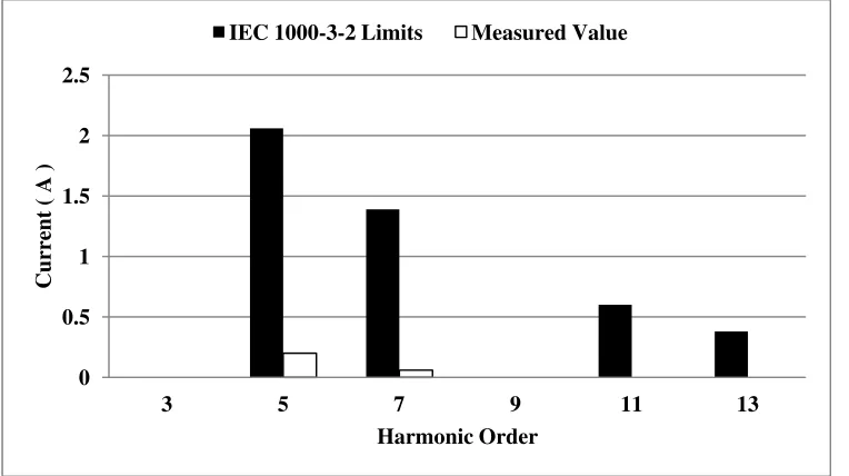
2.16 Input current harmonic at Vin = 230 Vrms , Po=1000W compared to
IEC1000-3-2 Class A
48
2.17 Input current harmonic at Vin = 100 Vrms , Po=1000W compared to
IEC1000-3-2 Class A
48
3.1 Proposed single-stage three-level AC-DC converter 52
3.2 Effect of output inductor value Lo on dc bus capacitor voltage 54
3.3 Typical experimental waveforms 56
3.4 Typical experimental waveforms 57
3.5 Proposed single-stage three-level AC-DC converter 59
3.6 Typical waveforms for proposed converter 59
3.7 Modes of operation 63
3.8 Typical waveforms of a PWM three-level Converter 64
3.9 Typical waveforms of a PSM three-level converter 65
3.10 Efficiency of PWM and PSM three-level single-stage AC-DC converter 66
4.1 Proposed SSPFC converter with two controllers 69
4.2 Typical waveforms describing the modes of operation 70
4.3 Equivalent circuits for each operation stage for the converter 75
4.4 Typical experimental waveforms. (a) Top switch voltages Vgs1 and Vgs2
(b) Bottom switch voltages Vgs3 and Vgs4 (c) Primary voltage of the
main transformer (d) Input current and voltage
80
4.5 Proposed converter efficiency vs. load power 81
4.6 Input current harmonic at Vin = 100 Vrms , Po=1kW compared to
IEC1000-3-2 Class A
81
4.7 Input current harmonics at Vin = 230 Vrms , Po=1kW compared to
IEC1000-3-2 Class A standard.
xiii
5.1 Three-phase three-level proposed converter 85
5.2 Typical waveforms describing the modes of operation. 86
5.3 Mode 1 (t0 < t < t1) 87
5.4 Mode 2 (t1 < t < t2) 90
5.5 Mode 3 (t2 < t < t3) 92
5.6 Mode 4 (t3 < t < t4) 92
5.7 The procedure of steady state analysis for determining the dc bus voltage 96
5.8 Effect of output inductor value Lo on dc bus voltage
(Vin=208Vrms, Vo=48V, fsw=50kHz)
97
5.9 of input Inductor value Lin on DC Bus Voltage
(Vin=208Vrms, Vo=48V, fsw=50kHz)
98
5.10 Effect of transformer ratio value N on dc bus voltage (Vin=208Vrms, Vo=48V, fsw=50kHz)
99
5.11 Effect of input voltage Vin on dc bus voltage
(Vin=208Vrms, Vo=48V, fsw=50kHz)
100
5.12 Variation of PF for different values of auxiliary winding turns ratio[28]. 106
5.13 Experimental results 108
5.14 Experimental results for 50% of full load 109
5.15 Experimental results for 25% of full load 110
5.16 Converter efficiency with input voltage VLL-rms = 220 V. 111
5.17 Input current harmonic at Vin = 220Vrms(l-l) , Po=1.5 KW compared to
IEC1000-3-2 Class A standard
112
5.18 Input current harmonic at Vin = 220Vrms(l-l) , Po=0.75 KW compared to
IEC1000-3-2 Class A standard
112
5.19 Proposed interleaved three-stage three-level converter 113
5.20 Typical waveforms describing the modes of operation 114
5.21 Mode 1 (t0 < t < t1) 116
xiv
5.23 Mode 3 (t2 < t < t3) 117
5.24 Mode 4 (t3 < t < t4) 118
5.25 Mode 5 (t4 < t < t5) 118
5.26 Mode 6 (t5 < t < t6) 119
5.27 Mode 7 (t6 < t < t7) 120
5.28 Mode 8 (t7 < t < t8) 120
5.29 Interleaving between two input inductor currents 121
5.30 Steady-state characteristic curves (Vin=208Vrms, Vo=48V, fsw=100kHz) 124
5.31 Experimental results 131
5.32 Input current harmonic at Vin = 220Vrms(l-l) , Po=1.1 KW compared to
IEC1000-3-2 standard
132
5.33 Input current harmonic at Vin = 220Vrms(l-l) , Po=0.575 KW compared to
IEC1000-3-2 standard
133
5.34 Efficiency of the proposed converter at various output power 134
6.1 Three-level DC-DC converter for low input voltage applications 137
6.2 Modes of operation 140
6.3 Typical waveforms of a three-level converter 140
6.4 A phase-shifted, full-bridge DC-DC converter with clamping diodes [20] 146
6.5 Typical waveforms of a three-level converter (Vin = 400 V) 147
6.6 Efficiency of ZVS full-bridge and three-level converter 148
6.7 Half-bridge converter 151
6.8 Modified half-bridge converter 152
6.9 Proposed converter 154
6.10 Proposed converter with zero degree phase shift 155
xv
6.12 Proposed converter with ϕ degree phase shift 156
6.13 Waveforms with phase-shift control 157
6.14 Typical waveforms describing modes of operation 158
6.15 Mode 1 (t1 < t < t2) 159
6.16 Mode 2 (t2 < t < t3) 160
6.17 Mode 3 (t3 < t < t4) 162
6.18 Mode 4 (t4 < t < t5) 162
6.19 Mode 5 (t5 < t < t6) 164
6.20 Effect of series inductor on duty cycle 166
6.21 Effective duty cycle versus resonant inductance 167
6.22 Transformers turns ratio versus resonant inductance 168
6.23 Gate and drain-source waveforms for Po=60W 171
6.24 Transformer primary voltage and current waveforms (Po=60W) 172
6.25 Transformer secondary voltage waveforms (Po=900W) 172
6.26 Voltages of rectifier diodes (Po=900W) 173
6.27 Efficiency of the proposed converter at different output power 173
6.28 Current of a rectifier diode (Po=1200W) 174
xvi
AC Alternate Current
DC Direct Current
CCM Continuous Conduction Mode
DCM Discontinuous Conduction Mode
EMI Electro-Magnetic Interference
MOSFET Metal Oxide Silicon Field Effect Transistor
PF Power Factor
PFC Power Factor Correction
PWM Pulse Width Modulation
PSM Phase Shift Modulation
RMS Root Mean Square
SSPFC Single-Stage Power Factor Correction
THD Total Harmonic Distortion
ZCS Zero Current Switching
ZVS Zero Voltage Switching
ZVZCS Zero Voltage Zero Current Switching
xvii
v Volt
A Ampere
Vin Input Voltage
Vo Output Voltage
Iin Input Current
Io Output Current
Vrec Rectified AC Voltage
Vdc DC Voltage
Vab Differential Voltage Between Node ‘a’ and Node ‘b’
D Duty Cycle
fsw Switching Frequency
t Time
CO Output Capacitor
LO Output Inductor
Ro Output Resistive Load
Lin Input Inductance
Dx Diode x
Sx Diode x
µ Micro
k Kilo
H Henry
Chapter 1
1. Introduction
Power electronics is the application of semiconductor devices for the control and
conversion of electric power. Power electronic converters can be found in any application
that needs to modify a form of electrical energy (i.e. change its voltage, current or
frequency). They can be classified according to the type of the input and output. As a
result, power electronic converters can be;
• AC to DC (rectifier)
• DC to DC
• DC to AC (inverter)
• AC to AC
The main focus of the research for this thesis has been mainly on AC-DC with
so-called multilevel or three-level structures, with some of this work extended to DC-DC
converters. In this thesis, several new converter topologies are proposed, their
steady-state characteristics are determined by mathematical analysis, and their design is
examined. The feasibility of each proposed converter is confirmed with experimental
results obtained from a proof-of-concept prototype and the main points of the thesis are
summarized at the end.
1.1.
Single-Phase AC-DC Converters (Rectifiers)
AC-DC converters are typically used in many industrial and commercial
applications including personal computers, battery chargers, telecommunication power
supplies, etc. Switch mode AC-DC converters are the first block in any power conversion
system that supplies power from an AC source such as the utility mains to any load. An
AC-DC power supply should operate in such a way that the input current and voltage are
purely sinusoidal and in phase with each other to comply with harmonic standards and
1000-3-2 [1000-3-2], IEC 1000-3-4 [3] and IEEE-519-1991000-3-2 [4]. As a result, power factor correction
(PFC) techniques are typically used in AC-DC power converters to ensure that these
standards are met.
The concept of power factor originated from the need to quantify how efficiently a
power converter utilizes the current that it draws from an AC power system. The true
power factor at the power converter is defined as the ratio of average power to apparent
power, or
=
(1.1)
If the power factor is less than one, they have to supply more current to the power
converter for a given amount of power use.
1.1.1.
Power Factor Correction Techniques
There are several PFC techniques that can be used to remove current harmonics
and thus improve the overall system power factor. The two main methods to eliminate or
at least reduce the input line current harmonics are
• Passive power factor correction
• Active power factor correction
1.1.1.1. Passive Power Factor Correction
One of the simplest and most straightforward methods to reduce input current
harmonics is by using passive circuits. A passive circuit consisting of passive reactive
elements can be located either at the input or at the output side of the input rectifier of an
AC-DC converter. Several passive PFC techniques have been investigated in the
literature, such as adding an LC filter at the output of the diode bridge rectifier, as shown
in Fig.1.1. Passive PFC techniques have several advantages and disadvantages. High
efficiency, low EMI and simple implementation are the advantages of these techniques,
but the main drawback is that they make the converter heavy and bulky. This drawback
1.
the input current drawn by the
the input voltage waveform; therefore, the input power factor is almost unity. Activ
has many advantages over passive PFC such as higher power factor, lower harmonic
content, smaller converter size due to the ability to use high switching frequencies, and
lighter weight. Active PFC methods, however, are more difficult to implement th
passive PFC methods because of the challenges involved in designing an active power
converter [5].
transformer isolation: two
techniques are discussed below.
two converter stages:
conversion stage Fig.1.1.
.1.1.2. Active Power Factor Correction
Active power factor correction (PFC) techniques use switching converters to shape
the input current drawn by the
the input voltage waveform; therefore, the input power factor is almost unity. Activ
has many advantages over passive PFC such as higher power factor, lower harmonic
content, smaller converter size due to the ability to use high switching frequencies, and
lighter weight. Active PFC methods, however, are more difficult to implement th
passive PFC methods because of the challenges involved in designing an active power
converter [5].
There are
transformer isolation: two
techniques are discussed below.
A. Two-Stage PFC Converter
Typical
two converter stages:
conversion stage
Two-stage AC
Active Power Factor Correction
Active power factor correction (PFC) techniques use switching converters to shape
the input current drawn by the
the input voltage waveform; therefore, the input power factor is almost unity. Activ
has many advantages over passive PFC such as higher power factor, lower harmonic
content, smaller converter size due to the ability to use high switching frequencies, and
lighter weight. Active PFC methods, however, are more difficult to implement th
passive PFC methods because of the challenges involved in designing an active power
converter [5].
There are two general types of
transformer isolation: two
techniques are discussed below.
Stage PFC Converter
Typical AC-DC power converters with transformer isolation are implemented with
two converter stages: an
conversion stage. A block diagram
AC-DC PWM converter with diode rectifier/
Active Power Factor Correction
Active power factor correction (PFC) techniques use switching converters to shape
the input current drawn by the AC-DC
the input voltage waveform; therefore, the input power factor is almost unity. Activ
has many advantages over passive PFC such as higher power factor, lower harmonic
content, smaller converter size due to the ability to use high switching frequencies, and
lighter weight. Active PFC methods, however, are more difficult to implement th
passive PFC methods because of the challenges involved in designing an active power
two general types of
transformer isolation: two-stage PFC techniques and single
techniques are discussed below.
Stage PFC Converter
power converters with transformer isolation are implemented with
an AC-DC conversion (rectifying) stage and an isolated
A block diagram of a two
PWM converter with diode rectifier/
Active Power Factor Correction
Active power factor correction (PFC) techniques use switching converters to shape
DC converter so that it is sinusoidal and in phase with
the input voltage waveform; therefore, the input power factor is almost unity. Activ
has many advantages over passive PFC such as higher power factor, lower harmonic
content, smaller converter size due to the ability to use high switching frequencies, and
lighter weight. Active PFC methods, however, are more difficult to implement th
passive PFC methods because of the challenges involved in designing an active power
two general types of active PFC for an
stage PFC techniques and single
power converters with transformer isolation are implemented with
conversion (rectifying) stage and an isolated
of a two-stage ac
PWM converter with diode rectifier/
Active power factor correction (PFC) techniques use switching converters to shape
converter so that it is sinusoidal and in phase with
the input voltage waveform; therefore, the input power factor is almost unity. Activ
has many advantages over passive PFC such as higher power factor, lower harmonic
content, smaller converter size due to the ability to use high switching frequencies, and
lighter weight. Active PFC methods, however, are more difficult to implement th
passive PFC methods because of the challenges involved in designing an active power
active PFC for an
stage PFC techniques and single-stage PFC techniques. The
power converters with transformer isolation are implemented with
conversion (rectifying) stage and an isolated
stage ac-dc converter
PWM converter with diode rectifier/LC
Active power factor correction (PFC) techniques use switching converters to shape
converter so that it is sinusoidal and in phase with
the input voltage waveform; therefore, the input power factor is almost unity. Activ
has many advantages over passive PFC such as higher power factor, lower harmonic
content, smaller converter size due to the ability to use high switching frequencies, and
lighter weight. Active PFC methods, however, are more difficult to implement th
passive PFC methods because of the challenges involved in designing an active power
active PFC for an AC-DC
stage PFC techniques. The
power converters with transformer isolation are implemented with
conversion (rectifying) stage and an isolated
dc converter is shown in Fig.
LC filter front.
Active power factor correction (PFC) techniques use switching converters to shape
converter so that it is sinusoidal and in phase with
the input voltage waveform; therefore, the input power factor is almost unity. Active PFC
has many advantages over passive PFC such as higher power factor, lower harmonic
content, smaller converter size due to the ability to use high switching frequencies, and
lighter weight. Active PFC methods, however, are more difficult to implement th
passive PFC methods because of the challenges involved in designing an active power
DC converter with
stage PFC techniques. The
power converters with transformer isolation are implemented with
conversion (rectifying) stage and an isolated DC
shown in Fig.1.2. Active power factor correction (PFC) techniques use switching converters to shape
converter so that it is sinusoidal and in phase with
e PFC
has many advantages over passive PFC such as higher power factor, lower harmonic
content, smaller converter size due to the ability to use high switching frequencies, and
lighter weight. Active PFC methods, however, are more difficult to implement than
passive PFC methods because of the challenges involved in designing an active power
converter with
stage PFC techniques. These
power converters with transformer isolation are implemented with
DC-DC
AC-DC boost converter is used in the rectifying stage for most applications and it
actively shapes the input line current so that it is almost sinusoidal, with a harmonic
content compliant with agency standards. The input current can either be discontinuous
or continuous. The DC-DC converter is used to regulate the output voltage and it can be a
forward, a flyback or any other step down isolated DC-DC converter.
Fig.1.2. Block diagram of standard two-stage PFC AC-DC converter.
B. Single-Stage PFC Converter
Although two-stage PFC converters are attractive because they can operate with a
high input power factor, they can be expensive because they have two switch-mode
converters in their topologies. The cost and complexity of the overall two stage converter
has led to the emergence of single-stage power-factor-corrected (SSPFC) converters.
Efforts have been made to develop smaller converters with fewer switches that can
comply with regulatory agency standards and be more cost effective than two-stage
converters, with the same performance. SSPFC circuits are required to provide the
features of both the power factor correction in addition to those of the DC-DC converter
cascaded with it.
1.1.2.
Review of Single-Phase Single-Stage PFC Converters
There have been numerous publications about SSPFC converters, particularly for
low-power AC-DC flyback and forward converters [6]–[24]. These cheaper and simpler
converters are widely used in industry and their properties and characteristics have been
Diode Bridge
Power Factor Correction
Circuit
DC-DC
Converter Load
well
converters, however, has pro
fewer publications [25]
as belonging among the following types:
well established. Research on the topic of higher power
converters, however, has pro
fewer publications [25]
Previously proposed single
as belonging among the following types:
• Resonant converters:
and capacitors that are connected in series and/or parallel to the primary of their
power transformer [27], [32]. Th
frequency control. As a result, it
their magnetic components) as they must be able to operate over a wide range of
switching frequency.
• Current
to the input of the full
Although they can achieve a near
storage capacitor across the primary
of high voltage overshoots and ringi
capacitor also causes the output voltage to have a large low
ripple that limits their application.
Fig.1.3. Boost
established. Research on the topic of higher power
converters, however, has pro
fewer publications [25]-[32].
Previously proposed single
as belonging among the following types:
Resonant converters:
and capacitors that are connected in series and/or parallel to the primary of their
power transformer [27], [32]. Th
frequency control. As a result, it
their magnetic components) as they must be able to operate over a wide range of
switching frequency.
Current-fed PWM converters:
to the input of the full
Although they can achieve a near
storage capacitor across the primary
of high voltage overshoots and ringi
capacitor also causes the output voltage to have a large low
ripple that limits their application.
3. Boost-based current
established. Research on the topic of higher power
converters, however, has proved to be more challenging, and
[32].
Previously proposed single-stage
as belonging among the following types:
Resonant converters: These converters have resonant elements such as inductors
and capacitors that are connected in series and/or parallel to the primary of their
power transformer [27], [32]. Th
frequency control. As a result, it
their magnetic components) as they must be able to operate over a wide range of
switching frequency.
fed PWM converters:
to the input of the full-bridge circuit; one such converter is shown in
Although they can achieve a near
storage capacitor across the primary
of high voltage overshoots and ringi
capacitor also causes the output voltage to have a large low
ripple that limits their application.
based current-fed AC
established. Research on the topic of higher power
ved to be more challenging, and
stage AC-DC
as belonging among the following types:
These converters have resonant elements such as inductors
and capacitors that are connected in series and/or parallel to the primary of their
power transformer [27], [32]. They must be controlled
frequency control. As a result, it is difficult
their magnetic components) as they must be able to operate over a wide range of
fed PWM converters: These converters have a boost inductor connected
ridge circuit; one such converter is shown in
Although they can achieve a near-unity input power factor, they lack an energy
storage capacitor across the primary-side dc bus, which can result in the appearance
of high voltage overshoots and ringing across the dc bus. The lack of such a
capacitor also causes the output voltage to have a large low
ripple that limits their application.
AC-DC PWM integrated full established. Research on the topic of higher power AC
ved to be more challenging, and
full-bridge conve
These converters have resonant elements such as inductors
and capacitors that are connected in series and/or parallel to the primary of their
ey must be controlled
difficult to optimize their design (especially
their magnetic components) as they must be able to operate over a wide range of
These converters have a boost inductor connected
ridge circuit; one such converter is shown in
unity input power factor, they lack an energy
side dc bus, which can result in the appearance
ng across the dc bus. The lack of such a
capacitor also causes the output voltage to have a large low
PWM integrated full
AC-DC
single-ved to be more challenging, and thus there have been much
bridge converters can be classified
These converters have resonant elements such as inductors
and capacitors that are connected in series and/or parallel to the primary of their
ey must be controlled using variable switching
to optimize their design (especially
their magnetic components) as they must be able to operate over a wide range of
These converters have a boost inductor connected
ridge circuit; one such converter is shown in
unity input power factor, they lack an energy
side dc bus, which can result in the appearance
ng across the dc bus. The lack of such a
capacitor also causes the output voltage to have a large low-frequency 120
PWM integrated full-bridge converter [26] -stage full-bridge
thus there have been much
rters can be classified
These converters have resonant elements such as inductors
and capacitors that are connected in series and/or parallel to the primary of their
using variable switching
to optimize their design (especially
their magnetic components) as they must be able to operate over a wide range of
These converters have a boost inductor connected
ridge circuit; one such converter is shown in Fig.
unity input power factor, they lack an energy
side dc bus, which can result in the appearance
ng across the dc bus. The lack of such a
frequency 120
bridge converter [26] bridge
thus there have been much
rters can be classified
These converters have resonant elements such as inductors
and capacitors that are connected in series and/or parallel to the primary of their
using variable
switching-to optimize their design (especially
their magnetic components) as they must be able to operate over a wide range of
These converters have a boost inductor connected
Fig. 1.3.
unity input power factor, they lack an
energy-side dc bus, which can result in the appearance
ng across the dc bus. The lack of such a
frequency 120-Hz
• Voltage
capacitor connected across their primary
Fig.1.4. These converters do not have the drawbacks of resonant and current
SSPFC converters. They operate with
capacitor prevents voltage overshoots and ringing from appearing across the dc bus
and keeps
(b)
Voltage-fed PWM
capacitor connected across their primary
4. These converters do not have the drawbacks of resonant and current
SSPFC converters. They operate with
capacitor prevents voltage overshoots and ringing from appearing across the dc bus
keeps the 120-Hz ac component from appearing at the output.
(
) Voltage-fed PWM full
Fig.1.4.
fed PWM converters:
capacitor connected across their primary
4. These converters do not have the drawbacks of resonant and current
SSPFC converters. They operate with
capacitor prevents voltage overshoots and ringing from appearing across the dc bus
Hz ac component from appearing at the output.
(a) Voltage-fed PWM full
fed PWM full
Some voltage
converters: These converters have a large energy
capacitor connected across their primary-side dc bus [26], [28]
4. These converters do not have the drawbacks of resonant and current
SSPFC converters. They operate with fixed switching frequency, and the bus
capacitor prevents voltage overshoots and ringing from appearing across the dc bus
Hz ac component from appearing at the output.
fed PWM full
fed PWM full-bridge converter with auxiliary winding [2
voltage-fed PWM full
These converters have a large energy
side dc bus [26], [28]
4. These converters do not have the drawbacks of resonant and current
fixed switching frequency, and the bus
capacitor prevents voltage overshoots and ringing from appearing across the dc bus
Hz ac component from appearing at the output.
fed PWM full-bridge converter [26]
bridge converter with auxiliary winding [2
fed PWM full-bridge converters
These converters have a large energy
side dc bus [26], [28]-[31], as shown in
4. These converters do not have the drawbacks of resonant and current
fixed switching frequency, and the bus
capacitor prevents voltage overshoots and ringing from appearing across the dc bus
Hz ac component from appearing at the output.
bridge converter [26]
bridge converter with auxiliary winding [2
bridge converters.
These converters have a large energy-storage
[31], as shown in
4. These converters do not have the drawbacks of resonant and current
fixed switching frequency, and the bus
capacitor prevents voltage overshoots and ringing from appearing across the dc bus
bridge converter with auxiliary winding [28]
storage
[31], as shown in
4. These converters do not have the drawbacks of resonant and current-fed
fixed switching frequency, and the bus
Although voltage-fed, single-stage PWM full-bridge converters seem to be the most
promising single-stage converters, they have disadvantages that have limited their use.
Most of these drawbacks are because
They are controlled by a single-controller and the dc bus voltage is left
unregulated;
They are implemented with two-level topologies that subject the converter components to high voltage stresses.
Due to these disadvantages, voltage-fed converters have the following drawbacks:
• The primary-side dc bus voltage of the converter may become excessive under high-input-line and low-output-load conditions. Since the dc bus voltage is left
unregulated, it is dependent on the converter’s input line and output load
operating conditions and component values. The high dc bus voltage results in
the need for higher voltage rated devices and very large bulk capacitors for the
dc bus. For example, the converters in [26], [28]-[29] have a dc bus voltage of
600 V.
• The input power factor of a single-stage voltage-fed converter is not as high as that of current-fed converters. For example, the converter proposed in [28] has
an input current that is neither continuous nor discontinuous, but is
“semi-continuous” with a considerable amount of distortion.
• The converter operates with an output inductor current that is discontinuous for all operation conditions. This results in the need for components that can handle
high peak currents, and additional output filtering to remove ripple [26]-[32].
Most of the drawbacks of voltage-fed SSPFC PWM converters are due to the fact
that their switches can be exposed to very high voltages (> 800 V). The converter can be
inductor, but doing so results in the above-mentioned drawbacks. If the converter can
somehow be designed so that its switches are exposed to less voltage, then there will be
less need to degrade the performance of the converter.
DC-AC multilevel converters that limit the voltage that their switches are exposed
to half the dc bus voltage have been proposed in the power electronics literature and are
widely used in high voltage, low switching frequency applications [33]-[39]. They limit
the switch voltage by using two bulk capacitors across the dc bus instead of one so that
the midpoint of the bulk capacitors, which is half the dc bus voltage, can be used as a
connection point in the converter. Attempts have been made by researchers to implement
voltage-fed multilevel AC-DC SSPFC converters as a way to relax the switch stress
limitations placed on non-multilevel (two-level) converters, such as in [27], [32] and
[40]-[45]. Although these converters are promising, they still have many of the problems
of previously proposed two-level SSPFC converters stated above such as distorted input
currents, discontinuous output currents, and the need for variable switching frequency.
1.2.
Three-Phase AC-DC Converters (Rectifiers)
In the later chapters of this thesis, an investigation will be made on whether
concepts that can be used for single-phase multilevel SSPFC converters can be extended
to higher power three-phase converters. In this section, previously proposed three-phase
SSPFC converters are reviewed and their drawbacks are stated.
1.2.1.
Review of Three-Phase Single-Stage PFC Converters
As with single-phase AC-DC power conversion, three-phase AC-DC power
conversion with input power factor correction (PFC) and transformer isolation is
typically done using two converter stages - a six-switch front-end ac-dc converter is used
to do the PFC and the dc bus voltage regulation and a four-switch full-bridge converter is
used to do the DC-DC conversion. This two-stage approach, however, is expensive and
complicated – even more so with three-phase converters than with single-phase
circuitry. Moreover, the converter must be operated with sophisticated control methods
that require the sensing of certain key parameters such as the input currents and voltages;
this is especially true if online PWM techniques are used.
Researchers have tried to reduce the cost and complexity of the standard converter
by modifying the AC-DC front end converters. Proposed alternatives have included:
• Using three separate AC-DC boost converter modules as shown in Fig.1. 5 [46]. Although the modularity of this approach makes it attractive, it needs three
switch-mode converters making it expensive and complex.
• Using a reduced switch AC-DC converter as shown in Fig.1.6 [47] as the first stage converter of a two-stage converter. Although this approach is cheaper than
conventional two-stage converters that use six-switch converters as the first
stage converter, it is only modestly so.
• Using a single-switch boost converter as shown in Fig.1.7 [48]. Although this approach reduces the cost of the first stage AC-DC converter considerably, two
separate switch-mode converters are still needed to perform three-phase AC-DC
power conversion with transformer isolation.
A Dc bus
B Full Wave Bridge dc-to- dc Full Wave Bridge dc-to- dc B C Full Wave Bridge dc-to- dc C A
Vo2
Vo1
Dc Bus
Fig.1.6. Reduced switch AC-DC converter [47].
C
S
D
L1
L
2
L3
Ca Cb Cc
La
Lb
Lc
Dc Bus
Fig.1.7. Single-switch boost converter [48].
Researchers have tried to further reduce the cost and complexity associated with
three-phase AC-DC power conversion and PFC by proposing single-stage converters that
integrate the functions of PFC and isolated DC-DC conversion in a single power
converter [49]-[58]. Several examples of single-stage converters are shown in Fig.1.8.
SSPFC that have limited their widespread use. Since these drawbacks are the same as
those discussed
SSPFC that have limited their widespread use. Since these drawbacks are the same as
those discussed
SSPFC that have limited their widespread use. Since these drawbacks are the same as
those discussed above for single
L Lb L L Lb L Fig.1.8. Three
SSPFC that have limited their widespread use. Since these drawbacks are the same as
above for single-phase converters
L5 C C La Lc Cin1 Cin2 La Lc
. Three-phase, single
SSPFC that have limited their widespread use. Since these drawbacks are the same as
phase converters r1 r3 C5 C6 (a) [50] S2 S3 Lm1 D5
D8 Lm2
(b) [51]
(c)[52]
phase, single-stage,
SSPFC that have limited their widespread use. Since these drawbacks are the same as
phase converters, they are not
. . r2 r4 . S1 S4 m1 Llk1 D7 D6 Llk2 m2 stage, AC-DC
SSPFC that have limited their widespread use. Since these drawbacks are the same as
re not discussed here.
Lo
Co
Lo
Co
converters.
SSPFC that have limited their widespread use. Since these drawbacks are the same as
discussed here.
o R
o R
Since the problems associated with three-phase SSPFC converters are similar to
those of single-phase SSPFC converters, it would seem that the solutions to these
problems would be similar as well. It is not automatic, however, that a single-phase
solution is appropriate for three-phase converter and vice versa, that a three-phase
solution can be implemented in a single-phase converter. This is because of the different
power levels and the fact that some topologies make use of the three-phase neutral
connection, which is not possible in single-phase converters.
1.3.
DC-DC Converters
Although the main focus of this thesis is on single-phase and three-phase
multilevel SSPFC converters, the use of multilevel converter concepts to improve the
performance of DC-DC full-bridge converters is investigated in this thesis. The
conventional two-level PWM full-bridge DC-DC converter is shown in Fig.1.9 [59]. The
way this converter works is as follows: The converter is in an energy-transfer mode when
a pair of diagonally opposed switches is on and the input DC voltage is impressed across
the transformer primary. The converter is in what is called a freewheeling mode of
operation when a pair of top switches (S1, S3) or bottom switches (S2, S4) is on and no
voltage is impressed across the transformer.
The converter operates with inherent soft switching (ZVS) turn-on of its switches
as available primary transformer energy is used to discharge the output capacitances of
the switches just before they are turned on. This is especially true when the converter is
operating under heavy load conditions, but not so for light load conditions as there is less
current flowing in the converter. Thus, less available transformer energy exists to
Fig.1.9. DC-DC isolated full-bridge converter [59].
1.3.1.
Review of DC-DC Converters
The two-level ZVS-PWM full-bridge (ZVS-PWM-FB) converter has two key
drawbacks that relate to efficiency:
• Circulating current
• Light load operation
These drawbacks are discussed in detail below.
1.3.1.1. Circulating Current
The load range over which the converter can operate with ZVS can be increased if
the amount of current that circulates in the transformer primary side of the converter is
also increased. This can be done by reducing the transformer primary to secondary turns
ratio or by adding some passive circuitry to the converter's primary that allows for more
current flow [60]-[64]. Increasing the amount of current circulating in the primary,
losses can offset any gains in efficiency due to ZVS. The end result is that although the
ZVS range may be extended, the load range over which there is an advantage for doing
so may not be as expected and heavy load efficiency may suffer as well.
A number of power electronics researchers have tried to take the opposite approach
and try to reduce primary circulating current in the ZVS-PWM-FB converter as much as
possible – particularly when the converter is in a freewheeling mode of operation when
either both of its top or both of its bottom switches are on. In this case, no voltage is
impressed across the transformer primary and current just circulates in the transformer
primary during this mode and contributes to conduction losses as no energy is transferred
to the output from the primary side and current. Researchers have thus proposed
zero-voltage-zero-current methods to eliminate freewheeling mode circulating current
[65]-[70], but this results in the loss of ZVS in some of the converter switches.
Circulating current and ZVS capability are inversely related as more circulating
current means a wider load range for ZVS operation as there is more energy available to
discharge the switch output capacitances, but more conduction losses and turn-off losses.
It is, therefore, standard practice for ZVS-PWM-FB converter designs that the range of
ZVS operation be limited to loads greater than 25%-50% full-load so that conduction
losses caused by circulating current do not become excessive.
1.3.1.2. Light Load Efficiency
As the use of electrical equipment and consumer electronics has exploded due to
the demands of society, the issue of light load efficiency has become more urgent in
recent years because of the need to conserve as much energy as possible. Consequently,
there has been increased interest by power electronics personnel to improve light load
efficiency of their converters. What this means is the standard practice for
ZVS-PWM-FB converter designs that the range of ZVS operation be limited to loads greater than
25%-50% full-load is becoming less acceptable.
When the converter is operating with a light load, there is less current flowing in
capacitances of the switches. This means that the converter switches do not turn on with
ZVS and thus have switching losses. Since the losses caused by the energy that is stored
in the switch output capacitances and dissipated in the switches when they are turned on
are fixed, they become dominant when the converter operates with light load and thus the
ZVS-PWM-FB converter has poor efficiency.
It was proposed in [59] to improve light load efficiency by adding a separate
optimally designed "mini-converter" to the main converter that would operate only when
under light load conditions in place of the main power converter. Although this approach
did improve light load efficiency significantly, it did so at the expense of increased cost
and complexity as the mini-converter required two additional active switches and needed
to be operated with sophisticated control methods.
1.4.
Thesis Objectives
In order to mitigate the drawbacks that two-level converters have, new three-level
multilevel AC-DC and DC-DC converters are proposed in this thesis. The main
advantage that three-level converters have over two-level converters is that their main
power switches are exposed to half the voltage that the switches in two-level converters
are exposed to. This advantage can be used to improve converter efficiency and to
improve converter performance in general. The main objectives of this thesis are as
follows:
• To propose a new single-phase, single-controller, AC-DC multilevel converter that has improved steady-state characteristics and improved performance than
other previously proposed converters of the same type.
• To propose modifications to this new converter that result in improved performance.
• To determine how the new converter operates with a second controller that is dedicated to regulating its transformer primary-side DC bus voltage.
• To propose a new three-phase AC-DC multilevel converter that has inherent interleaved operation that reduces the input current ripple.
• To propose a new multilevel DC-DC converter that takes advantage of the multilevel concepts derived from the research to improve performance.
• To determine the steady-state characteristics of all new converters proposed in the thesis so that they can be properly designed.
• To derive design procedures for all new converters proposed in the thesis.
• To confirm the feasibility of all new converters proposed in this thesis with experimental results obtained from proof-of-concept prototypes.
1.5.
Thesis Outline
The thesis is comprised of the following six chapters. Following is a briefing of
each chapter;
In Chapter 2, a new three-level, single-stage single-phase power-factor-corrected
(SSPFC) AC-DC PWM converter that operates with a single controller is proposed. The
proposed converter can operate with universal input voltage (90– 265 Vrms) and with
better performance than previously proposed converters of the same type. The operation
of the new converter is explained in detail and analyzed, and its steady-state
characteristics were determined. The converter’s design is discussed and a design
procedure is established and demonstrated with an example. Experimental results
obtained from a prototype are presented to confirm the feasibility of the new converter
and its ability to meet IEC 1000-3-2 standards for electrical equipment.
In Chapter 3, two modifications to the SSPFC converter introduced in Chapter 2 are
proposed. The first modification is the addition of a simple auxiliary circuit that allows
the converter to operate with improved output characteristics without compromising its
light-load performance. The second modification is to make some change to the original
two modifications are discussed in the chapter and their effectiveness in improving
converter performance is confirmed with experimental results.
The operation of the single-stage converter proposed in Chapter 2 with two
controllers in examined in Chapter 4. The second controller is used to regulate the
intermediate dc bus voltage on the primary side of the main power transformer, which is
standard practice in two-stage AC-DC converters. The converter’s operation with two
controllers and the design of the converter is discussed in the chapter. The effect of the
second controller on the converter’s operation is studied based on experimental results
obtained from a prototype converter.
In Chapter 5, the single-phase converter proposed in Chapter 2 is modified for
three-phase operation to determine if the concepts and principles associated with this
converter can be extended to three-phase operation. The new three-phase converter is
then modified by implementing it with interleaved sections. The operation of both new
three-phase SSPFC multilevel converters are explained in detail and analyzed, their
steady-state characteristics are determined, and their design is examined discussed. The
feasibility of the converters is confirmed with experimental results obtained from
prototype converters.
The multilevel concepts examined in previous chapters of the thesis are used to
develop a new three-level DC-DC converter that is proposed in Chapter 6. In the chapter,
the basic operation of the converter is explained, its features are stated, and its design is
investigated. The feasibility of the converter is experimentally confirmed with results
obtained from a prototype converter.
In Chapter 7, the contents of the thesis are summarized, the conclusions that have
been reached as a result of the work performed in thesis are presented, and the main
contributions of the thesis are stated. The chapter concludes by suggesting potential
Chapter 2
2. Single-Phase Single-Stage Three-Level Power Factor
Correction AC-DC Converters
2.1. Introduction
Voltage-fed, single-stage power factor correction (SSPFC) full-bridge converters
are attractive because they cost less than two-stage converters, but their use has been
limited because of the drawbacks that they have. Most of these drawbacks are because
they are controlled by a single controller that regulates the output voltage so that the dc
bus voltage is left unregulated. As a result, the primary-side dc bus voltage of these
converters may become excessive under high-input-line and low-output-load conditions.
Measures can be taken to limit the dc bus voltage so that does not become excessive, but
these measures affect the performance of voltage-fed, SSPFC full-bridge converters in
several ways, including the following:
• The input power factor of a single-stage voltage-fed SSPFC converter is not as high as that of current-fed converters.
• The output inductor current of a single-stage voltage-fed SSPFC converter is discontinuous for all operation conditions, which results in higher secondary-side
component peak current stresses.
The performance of voltage-fed, SSPFC full-bridge converters can be improved if
the limit on the dc bus voltage (typically < 450 V) is relaxed. This is not something that
can be done for SSPFC full-bridge converters that are based on two-level topologies, but
this can be done for converters that are based on three-level, multilevel topologies as the
primary-side switching devices of these converters are exposed to half the peak voltage
stress that those of two-level converters are. As a result, the dc bus voltage limit can be
doubled for multilevel converters, but the peak voltage stress of the switches is the same
In this chapter, a new AC-DC SSPFC PWM multilevel converter is proposed. The
basic operation of the converter is explained as are the various modes of operation that
the converter goes through during a switching cycle. The steady-state characteristics of
the converter are determined by mathematical analysis and are used to develop a
procedure for the design of key converter components. The feasibility of the new
converter is confirmed with results that were obtained from an experimental prototype.
2.2. A New Single-Phase Single-Stage Three-Level Power
Factor Correction AC-DC Converter
One of the new AC-DC multilevel SSPFC converters that is proposed in this work
is shown in Fig.2.1. The proposed converter is a novel, efficient and cost effective
single-phase voltage-fed SSPFC that can operate with universal input voltage range (90– 265
Vrms) with wide output load variation (from 10% of full load to a full load that is greater
than 500 W), fixed frequency PWM control, excellent power factor, a continuous output
inductor current for load more than 50%, without its components being exposed to
excessive peak voltage stresses. This combination of features does not exist in the present
power electronics literature.
2.3.
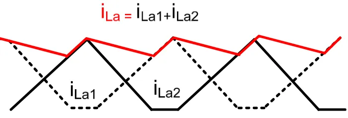
Operation of the Proposed Converter
The proposed converter, shown in Fig.2.1, consists of an AC input section, a
three-level DC-DC converter, and dc link circuitry that is based on auxiliary windings taken
from the main power transformer and that contains an inductor Lin and two diodes. The
dc link circuit acts like the boost switch in an AC-DC PFC boost converter. Whenever
two converter switches are ON, a voltage is impressed across each auxiliary winding so
that the voltage across one of the windings cancels out the voltage across the dc link
capacitors (sum of the voltage across C1 and C2). This is analogous to the boost switch
being ON and current in Lin (which can be considered to be the boost inductor) rises.
Whenever only one converter switch is ON, no voltage is impressed across any of the
Fig.2.1. Proposed single-stage three-level converter.
This is analogous to the boost switch being OFF and current in Lin falls. If the
converter is designed so that it operates with a constant duty cycle and a discontinuous
Lin current throughout the line cycle, then input PFC can be achieved without introducing
any significant low frequency component to the output as the peak current in Lin tracks
the sinusoidal wave shape of the rectified supply voltage.
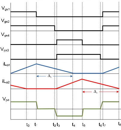
Typical converter waveforms are shown in Fig.2.2, and equivalent circuit diagrams
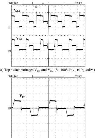
that show the converter’s modes of operation are shown in Fig.2.3 and 2.4 with the diode
rectifier bridge output replaced by a rectified sinusoidal source and thick lines
representing the paths of current conduction. The converter has the following modes of
s
∆
Fig.2.2. Typical waveforms describing the modes of operation.
Mode 1 (t0 < t < t1): During this mode, switches S1 and S2 are ON and energy from the
dc-link capacitor C1 flows to the output load. Since the auxiliary winding generates a
voltage that is equal to the total DC-link capacitor voltage (sum of C1 and C2), the voltage
across the auxiliary inductor is the rectified supply voltage.
This allows energy to flow from the AC mains into the auxiliary inductor during
this mode, and the auxiliary inductor current increases, according to
, = ,
(a) Mode 1 (t0 < t < t1)
(b) Mode 2 (t1 < t < t2)
(c) Mode 3 (t2 < t < t3)
(d) Mode 4 (t3 < t < t4)
where |vs,k| is the rectified AC supply voltage during switching cycle interval k. The
supply voltage can be considered to be constant within a switching cycle as the switching
frequency is much higher than the line frequency. The current in the auxiliary inductor
Lin at the end of Mode 1 is
,, = ,
.
2 2.2 Duty cycle, D, is defined as the time when S1 and S2 are both ON during the first half
cycle or when S3 and S4 are both ON during the second half cycle. These two cases
correspond to energy transfer modes of operation. Since D is defined with respect to a
half switching cycle Tsw/2 or 1/2fsw, (where fsw is the switching frequency) the duration
that is used in equ. (2.2) is D/(2fsw).
Similarly, the output inductor current can be expressed as;
=
2 ! −
# . 2.3
where Vbus is the average DC-link voltage, VL is the load voltage and N is the transformer
ratio between input and output (N = Npri/Nsec). If the output inductor current is
continuous then peak ripple current can be expressed as
∆ =
2 ! −
# . 2 2.4
Mode 2 (t1 < t < t2): S1 is OFF and S2 is ON during this mode. The energy stored in Lin
during the previous mode is completely transferred into the DC-link capacitor. The
amount of stored energy in the auxiliary inductor depends upon the rectified supply