Digital simulation of closed loop control of
bi-directional dc - dc converter
*
S.A. Elankurisil,. and** Dr. S.S. Dash*Research Scholar, Sathyabama University,
Chennai. India ** Professor & Head
Department of EEE SRM University,Chennai, India
Abstract:
This paper presents a closed loop control of isolated boost full bridge dc-dc converter for used in Medium and High power application. Zero voltage switching is applied in all switches. The dc input voltage is stepped up by using a boost converter. It is inverted using a fullbridge inverter. The transformer is used to produce a higher voltage in secondary voltage side The a.c. voltage is converted into d.c. voltage with the help of rectifier. The open loop model there is no possiblity of maintain a constant voltage with variation of input voltage. In closed loop system is maintain a constant voltage is applied with various value of input voltage. Matlab 7.3 version is used for simulating the open loop and closed loop full bridge dc – dc converter are verified. Isolated boost converter can operate at an input voltage of 24V and the output voltage 200-260 V and average efficiency of 89% at 55khz switching frequency.
Index term: Bidirectional power flow, zero voltage switching, Micro controller, full bridge, isolated boost converter.
I. Introduction:
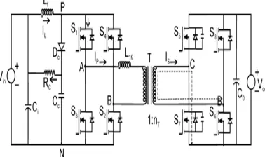
Isolated boost full bridge dc-dc converter is used for medium and high power application. It is an alternative source of electrical energy. Fig.1 shows the block diagram of isolated boost full bridge dc-dc converter. The input voltage is applied to the boost converter to boost the voltage. Full bridge inverter is used to convert the dc voltage into ac voltage.
The transformer is used to stepup the ac voltage and also isolate the low voltage and high voltage. Rectifier is converted into ac voltage into dc voltage. It is applied to the resistive load. In forward direction the low voltage side to high voltage side the circuit works in boost mode. In reverse direction high voltage side to low voltage side the circuit works in buck mode.
The hormonic current pollution of the ac power systems is being restrained by international standard [1]. A dual active full bridge dc–dc converter for high power bidirectional application [2]. A dual active half bridge softswitching bidirectional, avoiding voltage spike issue in a current fed inverter [3]. The converter operates in continous conduction mode with soft commutation of the control switches and constant frequency pulse width modulation [4-7].
Fig.1 Block Diagram of Closed Loop Control of Isolated Boost Full Bridge dc-dc converter
voltage with the variation of input. The closed loop system is maintained constant voltage with the variation of input voltage.
Fig 2 Isolated Boost Full bridge Dc-Dc Converter
II. Operating Principle:
The opeating principle are divided into two modes i) Energy storing mode ii) Energy transfering mode. At initial condition, the input voltage is applied to the inductor energy is stored in the inductor. S1-S4switches
are ON condition for the fraction of seconds. In boost mode opeation four ON and two OFF switches. The converter is operated in two modes inbetween the commutating mode is operated.
1. S1-S4 are turned ON. Inductor is stored energy corresponding current increases linearly. S7, D6 are ON
the current through the primary winding of the transformer is short circuted. To create a freewheeling flow part are S7, D6.
2. S6 can be turned ON after zero voltage condition.
3. S3, S4 are turned OFF. The voltage is charged quickly by the balance current upto the active
clamping. S7, D6 are remains ON.
4. At the condition IL–IP, after commutating ends and the converter is waiting for energy transfering
mode. S7, D6 are remains ON.
5. Secondary side of the transformer remains ON drops from zero. Energy is stored in inductor again.
6. S7 is turned OFF D5 is turned ON. D5 and S6 are transferring energy from primary side to the secondary
side of the converter. S5 is ON. Under zero voltage switching and prepares the next commutating
modes. Is=IL, Energy transfering mode ends. S5, D8 to create current free wheeling path to change its
direction.
7. D6- S5 remains ON until it resets to zero. After the resonate period. D8 forming a freewheeling path
and leakage current path through S5 – D8.
7. Again the cycle is repeated S1-S4 are turned ON.
Bidirectional
Symbol Definition
C Capacitor
V Voltage
R Resistance
ACPC Accelerated commutation for passive clamping
VIN input voltage
VO output voltage
Pin input power
Io output current
Lf Inductor
S1 S2 S3 S4 switches that act as an inverter bridge.
(VIN to VO boost mode)
(VO to VIN buck mode)
S5 S6 S7 S8 switches that act as rµectifier Bridge.
(Vin to Vo) and an inverter bridge in buck mode
(VO to Vin)
Ф flux
Dc – Cc - Rc Passive snubber designed for Boost mode
fs Switching frequency
IL Inductor current
L1k Transformer leakage Inductance
Ip Transformer primary current
Cc Snubber clamping capacitor
Is Transformer secondary current
Rc Clamping resistor
Dc Clamping diode
Ci input filter capacitor
N Negative Node
P Positive Node
A Node A
B Node B
C Node C
D Node D
T Main transformer
E1 Emf induced in primary
E2 Emf induced in Secondary
nT number of turns
Co output filter capacitor
Ts High frequency switching period.
δ duty cycle
∆I small current
III.Design Guide lines
Losses:
1.The conduction losses in the rectifier are the same for conventional PWM and ZVS PWM.
Prect = 4 (Iout / 2 Vf)
Vf is the forward drop for the rectifier diodes, assuming that a full bridge rectifier is used.
2. The conduction losses on the primary bridge diodes are. PD = Vdiode Iav
Vdiode is the forward voltage drop on the diodes and Iav is the average current.
3. The conduction losses due to channel resistance of the switches can be calculated as PQ = Ron Irms
To find parameters.
1. L = Voδ / f ∆I
2. Io = Vo / R
3. Po = Vo 2
/ R 4. E1 = 4.44 N1 Φf
5. E2 = 4.44 N2 Φf
Losses:
Transformer = 12 w Inductor = 5 w Resistor = 10 w
IV.Simulation results
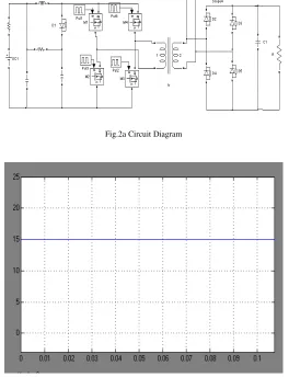
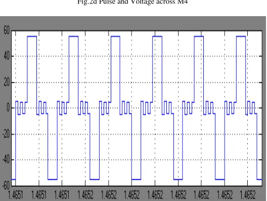
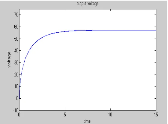
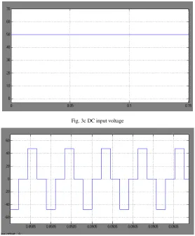
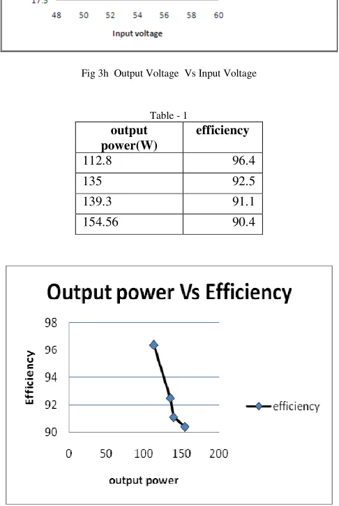
ZVS-PWM D.C. to D.C. converter is simulated using mat lab and the simulation results are presented. The primary side four MOSFET switches and four diodes is used in the secondary side of the transformer. The circuit model of isolated boost ZVS-PWM D.C to D.C. converter is shown in Fig 2a. DC input voltage is 15V as shown in fig2b. The square Pulse width is applied with constant frequency and voltage across M3 are shown in fig 2c. and M4 are shown in Fig 2d. The inverter output voltage is shown in Fig 2e. The transformer is stepped up the voltage and then converted A.C into D.C with capacitor is connected across the load output voltage across load is shown in Fig 2f. the four switches at the voltage fed inverter side arev also verified under soft swiching condition The harmonics across the inverter voltage is shown in Fig 2g. The D.C to D.C converter operating in buck mode is shown in Fig 3a. The driving pulses for MOSFETS M1 and M2 are shown in fig 3b. The dc input voltage is 50 voltages as shown in fig3c. The transformer primary voltage is shown in fig3d.The transformer secondary voltage is shown in fig 3e. The Output voltage is shown in Fig 3f. Variation of output with input for boost and buck modes are shown in Fig.3g & fig.3h. The output power with efficiency as shown in fig.3i.The open loop converter using a input voltage of 12v is simulated under the condition ,below
VIN = 15V, Co = 300µf , Vo =58V,δ = 0.5, Cc = 1500 µf , Rc =2000Ω, L= 350µH, f = 55khz
Boost Mode :
Fig.2a Circuit Diagram
Fig. 2c Pulse and Voltage across M3
Fig.2d Pulse and Voltage across M4
Fig. 2f DC output voltage
Fig.2g FFT ANALYSIS For voltage
Buck Mode :
Fig3b Driving pulses for M1 and M2
Fig. 3c DC input voltage
Fig. 3e transformer secondary voltage
Fig.3f DC Output voltage
Fig 3h Output Voltage Vs Input Voltage
Table - 1 output power(W)
efficiency
112.8 96.4
135 92.5
139.3 91.1
154.56 90.4
Fig.3i output power Vs Efficiency
Fig.4a. Closed loop circuit diagram
Fig.4b. Output voltage with disturbance
Conclusion
Bidirectional power flow control and conversion capability and with electrical. Isolation between the two sides through a transformer are evaluated for medium and high power application with consideration of device availability and a preliminary design study, a circuit configuration with the current fed converter on the LV low side and the voltage fed converter on the HV side is arranged the peak charging mode efficiency reaches 96% with full bridge version, but only 90% of full bridge converter is more efficient because it allows lower voltage devices to be used, and the active clamp circuit provides loss less operation. The open loop and closed simulation can be presented. The advantages of Boost converter are also obtained by adding Boost converter at the input side. This circuit is capable of performing D.C.to D.C. Conversion with high efficiency. The circuit using PI controller to maintain a constant with various value of input.
References
[1] T.S. Key and J.S. Lai, “IEEE and international harmonic standards impact on power Electronic design”, in Proc. Virgina Power Electron Sem (VPEC), 1988 PP, 39-45.
[2] Lizhizhu “A Novel soft commutation Isolated Boost Full bridge ZVS-PWM DC-DC converter for Biderectional High Power applications in IEEE Transactions on Power Electronics Vol.21, No.2, March 2006.
[3] Z Peng, Hui Li and Jack S.Kawler “New ZVS bidirectional DC-DC converter for fuel cell and battery application in IEEE transaction on power Electronics Vol.19 No.1, January 2004.
[5] C.M.C. Duarte and I.Barbi, “A family of ZVS-PWM active clamping D.C. to D.C. converters, Synthesis, analysis, design and experiemetnation”, ‘IEEE Trans, circuits system, vol 44, PP 698 – 704 Aug 1997.
[6] R.T. Bascope and I. Barbi, “a double ZVS-PWM active clamping forward converter in proc. IEEE Appl. Power Electronics Conf’ expo (APEC) 1999, PP 596-601.
[7] Zhu, Kurong Wang, Fred C. Lee, Jih-Shang-Lai, “ New Start UP schemes for Isolated boost full bridge boost converters, proc. IEEE Power Electronics trans 2003, PP 946-951.
[8] R. Watson, F.C. Lee, “A soft switched full bridge boost converter employing and active-clamp circuit”, in proc IEEE PSEC, 1986, PP 1948-1954.
[9] M. Zimmermann, G.D. Silva, A. Peres E. Deschamps, “PWM strategies for high voltage Isolated dc-dc converter for rectifier system”, IEEE Telecommunication conference, PP 415-420, Sep 2005.
[10] Elton pepa, “Adaptive control of a step up full bridge dc-dc converter for variable low input voltage applications. M.S. Thesis Department of Electrical Engg. Virginia Polytechnic institute and state university, Virginia, USA, 2004.
[11] Lizhizhu, “A Novel soft commutating Isolated Boost full bridge ZVS-PWM dc-dc converter for Bidirectional High power Application”, IEEE Transactons on power Electronics Vol 21 No.2, March 2006.
Biographical notes.
S.A.Elankurisil has obtained B.E degree from Madras university and M.E Degree from Sathyabama university in the years 1998 and 2006 respectively. He has twelve years of teaching experience. He is presently a research scholar at sathyabama university. He is a life member of I.S.T.E.