Nanotechnology, Science and Applications
Dove
press
O r I g I N A L r e S e A r c H open access to scientific and medical research
Open Access Full Text Article
Power optimized variation aware dual-threshold
SrAM cell design technique
Aminul Islam1 Mohd Hasan2
1Department of electronics and
communication engineering, Birla Institute of Technology, Mesra, ranchi, Jharkhand, India; 2Department
of electronics engineering, Aligarh Muslim University, Aligarh, Uttar Pradesh, India
correspondence: Aminul Islam Department of electronics and communication engineering, Birla Institute of Technology Tel +91 571 272 1141 Fax +91 571 272 1148
email [email protected]
Abstract: Bulk complementary metal-oxide semiconductor (CMOS) technology is facing enormous challenges at channel lengths below 45 nm, such as gate tunneling, device mismatch, random dopant fluctuations, and mobility degradation. Although multiple gate transistors and strained silicon devices overcome some of the bulk CMOS problems, it is sensible to look for revolutionary new materials and devices to replace silicon. It is obvious that future technology materials should exhibit higher mobility, better channel electrostatics, scalability, and robustness against process variations. Carbon nanotube-based technology is very prom-ising because it has most of these desired features. There is a need to explore the potential of this emerging technology by designing circuits based on this technology and comparing their performance with that of existing bulk CMOS technology. In this paper, we propose a low-power variation-immune dual-threshold voltage carbon nanotube field effect transistor (CNFET)-based seven-transistor (7T) static random access memory (SRAM) cell. The proposed CNFET-based 7T SRAM cell offers ∼1.2× improvement in standby power, ∼1.3× improvement in read delay, and ∼1.1× improvement in write delay. It offers narrower spread in write access time (1.4× at optimum energy point [OEP] and 1.2× at 1 V). It features 56.3% improvement in static noise margin and 40% improvement in read static noise margin. All the simulation measurements are taken at proposed OEP decided by the optimum results obtained after exten-sive simulation on HSPICE (high-performance simulation program with integrated circuit emphasis) environment.
Keywords: carbon nanotube field effect transistor (CNFET), chirality vector, random dopant fluctuation (RDF), SNM
Introduction
The continuous growth of recent mobile and portable devices and applications has caused a tremendous thrust for low power circuit design. Static random access memory (SRAM) is a highly used circuit in modern processors and occupies a considerable portion of chip area. It is a major contributor to the total power consumption. Various methods and techniques, such as SRAM’s cell voltage collapsing, increasing virtual
ground,1–3 have been applied successfully in the low power and performance region
of the design spectrum. However, in some applications where ultralow power con-sumption is the primary requirement and performance is of secondary importance, a more aggressive approach is warranted. Such applications range from various medical applications (such as implantable pacemakers, defibrillators, hearing aids) to the emerging mobile applications (such as wearable wristwatch computers, wireless sensor nodes, radio-frequency identification [RFID] tags). However, such minimum
Nanotechnology, Science and Applications downloaded from https://www.dovepress.com/ by 118.70.13.36 on 24-Aug-2020
For personal use only.
Number of times this article has been viewed
This article was published in the following Dove Press journal: Nanotechnology, Science and Applications
Dovepress
Islam and Hasan
energy operation is only possible in the subthreshold region. The pitfall of subthreshold design and near-threshold com-puting is increased sensitivity to parameter variation. These fluctuations are more pronounced in minimum-geometry devices commonly used in area-constraint circuits such as SRAM cells.4 The static noise margin (SNM) model5 assumes
identical device threshold voltage across all cell transistors, making it unsuitable for predicting the effects of threshold voltage mismatch between adjacent transistors within a cell due to random dopant fluctuation (RDF). Therefore, reinves-tigation is required to reassess SNM in scaled technologies to ensure stability of the SRAM cell. Process, voltage, and tem-perature (PVT) variations can be mitigated by the adaptive body biasing design technique,6 but its effect diminishes with
technology scaling.7 SRAM is a highly used circuit of modern
chips. As per the prediction of the International Technology Roadmap For Semiconductors (ITRS), an embedded cache will occupy 90% of a system on a chip by 2013.8 Hence, the
design and reinvestigation of the SRAM cell in terms of its design metrics is not only vital, but its robustness against PVT variations is necessary in a nanoscale regime such as 22 nm technology node.
Research over the past 5 years has demonstrated that the minimum-energy point (MEP) of the energy-delay curve is attractive. The penalty for operating at the MEP is substantial.
We can gain 10× in performance by increasing energy by
20% above MEP. The most dominant optimization variable
around MEP is the supply voltage.9 We explored the design
space above MEP and below VDD (supply voltage) to achieve
higher performance at the cost of minimal delay. In this paper, we make the following contributions:
1. In view of the aforesaid ultralow power requirement and variation issue, we propose a fully differential dual- diameter carbon nanotube field effect transistor (CNFET)-based seven-transistor (7T) SRAM cell (here-after called CNFET-7T) and compare its performance at proposed optimum energy point (OEP), defined as low-power dissipation point, with its complementary metal-oxide semiconductor (CMOS) counterpart. 2. We demonstrate that the proposed design outperforms its
CMOS counterpart CMOS-based 7T SRAM cell (here-after called 7T) in terms of static noise margin (SNM) and read-static-noise margin (RSNM).
3. We establish that the proposed design offers improved write access time variation exhibiting its immunity against PVT variation. This is achieved by proper selec-tion of chirality vector for appropriate transistor in the proposed design.
4. In standby mode, SRAM cells are inactive and consume power for data retention due to various leakage components. We investigate leakage power consumed by proposed design and 7T.
Estimation of threshold
voltage of CNFET
Sixty-five nanometer technology became common after 2006, and 45 nm technology was announced in 2007. As CMOS continues to scale deeper into the nanoscale, various nonide-alities cause the I–V characteristics of nanoscaled devices to be substantially different from that of long-channel devices. It becomes more difficult to further improve device/ circuit performance by reducing the physical gate length. As CMOS reaches its scaling limits, development of alter-native technologies is necessary to further improve device/ circuit performance by reducing the physical gate length.10
Nanotechnology-based fabrication is expected to offer the extra density and potential performance to take electronic circuits to the next step. Several nanoscale electronic devices have been demonstrated in the recent past by researchers, some of the most promising being CNFET. The CNFETs can be scaled down to 10-nm channel length and 4-nm channel width, thereby enhancing throughput in terms of speed and power compared with metal-oxide-semiconductor field-effect transistor (MOSFET). The shortcoming of the CNFET-based design is that there are some fabrication issues, which are likely to be overcome in the near future. The performance of CNFET has significantly improved since the first fabricated device in 1998. Most of the fabrication issues like position-ing and alignment of carbon nanotubes (CNTs) along with the presence of metallic CNTs have been solved.11−15 The
impact of CNT diameter and source/drain doping variations is not significant.16,17 Moreover, CNFET can be fabricated
using the existing silicon MOSFET infrastructure and it can
also be integrated with silicon MOSFET on the same chip.18
Most of the fabrication issues have been solved and CNFET technology is promising. It is also important to investigate the potential of systems designed in upcoming technology for their rapid commercialization once the technology matures.
Most of the fundamental limitations of traditional silicon MOSFETs are mitigated in CNFET. With ultralong (∼1 µm) mean free path for elastic scattering, a ballistic or near- ballistic transport can be obtained with the use of CNTs under low voltage bias to achieve the ultimate device performance.19−21 Its quasi-1D structure provides better
electrostatic control over the channel region than 3D devices
Nanotechnology, Science and Applications downloaded from https://www.dovepress.com/ by 118.70.13.36 on 24-Aug-2020
Dovepress Power optimized variation aware dual-threshold SrAM cell design technique
(for example, bulk CMOS) and 2D device (for example, fully depleted SOI (silicon on insulator)) structures.22 Ballistic
transport operation and low IOFF (OFF-current) make the CNFET a suitable device for high performance and increased integration. CNTs are categorized into single-walled CNTs (SWCNTs) and multiwalled CNTs (MWCNTs). Most SWCNTs have a diameter of close to 1 nm, with a tube length that can be many millions of times longer. The structure of a SWCNT can be conceptualized by wrapping a 1-atom-thick layer of graphite called graphene into a flawless cylinder. SWCNT-based CNFETs are used in this design.
Properties of a SWCNT depend on its chirality (n1, n2): the direction in which it is rolled up. The CNT acts as metal if
n1= n2 or (n1 – n2)/3 = i, where i is an integer. Otherwise, the
CNT works as semiconductor. The DCNT (diameter of CNT)
is estimated using its chirality vector (n1, n2) as:23−26
DCNT =πa n n n n12+ 22+ 1 2 (1)
The Vt (threshold voltage) of CNFET can be approxi-mated to the first order as the half bandgap, which is an inverse function of the CNT diameter (DCNT):23
V E
q
aV qD
t g
CNT
≈ =
2 1
3
π (2)
where Eg = energy gap, q = electronic charge, a = √3d =
2.49 Å is the lattice constant (where d ≈ 1.44 Å is the inter-carbon-atom distance) and Vπ= 3.033 eV is the carbon
π–to-π bond energy in the tight bonding model. The use of appropriate DCNT and hence Vt of CNFETs is a critical piece of our design strategy. In this work, dual-Vt and dual-diameter CNFETs are used using chiral vector values (11, 0) and (13, 0). The DCNT of the CNFET with chiral vector value (11, 0) and (13, 0) are computed using (1) to be 0.8719 nm (MP1, MP2, MN1, MN2 and MN4 of CNFET-7T) and 1.03 nm (for MN3
and MN5 of CNFET-7T) respectively. The Vt of the CNFET
with chiral vector value of (11, 0) and (13, 0) are computed using (2) to be 0.5018 V and 0.4246 V respectively.
Compared with CMOS circuits, the CNFET circuits with 1–10 CNTs per device is about 2 to 10 times faster.10,25
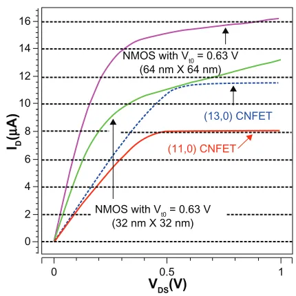
CNTs are placed on substrate having a dielectric constant of Ksub= 4. The tubes are separated by a high-k (Hi-k) material called HfO2 (hafnium oxide) having a dielectric constant of Kox= 16 and thickness of tox= 4 nm. Other important device and technology parameters related to CNFET are tabulated in Table 1. The I–V characteristics of employed CNFETs with chirality vector (11, 0) and (13, 0) and NMOS (n-type metal-oxide-semiconductor) with zero bias threshold
voltage, Vtn0= 0.63 V are plotted in Figure 1. P-type CNFET used in the proposed design has I–V characteristics with opposite polarity (not shown). The threshold voltages of N-CNFET are estimated using (1) and (2) with chirality vec-tor ranging from (7, 0) to (36, 0). First, the DCNT are estimated substituting the value of the constant π= 3.142, the value of the lattice constant a = 2.49 Å, and the value of n1 ranging from 7 to 36 keeping n2= 0. Next, the threshold voltage Vt is estimated substituting the value of a = 2.49 Å, the value of the carbon π–π bond energy Vπ= 3.033 eV, the value of electronic charge q = 1.6 × 10⁻¹⁹ C, and the estimated value
of DCNT. The estimated values of threshold voltage for each value of n1 ranging from 7 to 36 are plotted in Figure 2. The
plot in Figure 2 shows two end points with Vt= 0.78857 V
at n1= 7 and Vt= 0.153 V at n1= 36. Two other important points in this plot are (11, 0.5018) and (13, 0.4246) which indicate Vt= 0.5018 V at n1= 11 and Vt= 0.4246 V at n1= 13. These are the threshold voltages of CNFETs used in the
pro-posed design. The threshold voltage (Vt) of P-type CNFET
employed in this design has an opposite polarity.27
Table 1 Device and technology parameters of cNFeT
Parameter Description Value
Lch Physical channel length 22 nm
Wg The width of metal gate (sub_pitch) 6.4 nm Kox Dielectric constant of high-K gate oxide 16
(n1, n2) chirality of the tube (11, 0) (13, 0)
n_cNT Number of tube 1
(11,0) CNFET (13,0) CNFET
NMOS with Vt0 = 0.63 V
(64 nm X 64 nm)
NMOS with Vt0 = 0.63 V (32 nm X 32 nm)
1 0.5
0
VDS(V)
ID
(
µ
A)
16
14
12
10
8
6
4
2
0
Figure 1 comparison of I–V characteristics of NMOS and cNFeT.
Abbreviations: cNFeT,carbon nanotube field effect transistor; NMOS, n-type metal-oxide-semiconductor.
Nanotechnology, Science and Applications downloaded from https://www.dovepress.com/ by 118.70.13.36 on 24-Aug-2020
Dovepress
Islam and Hasan
Proposed CNFET-based
7T SRAM cell
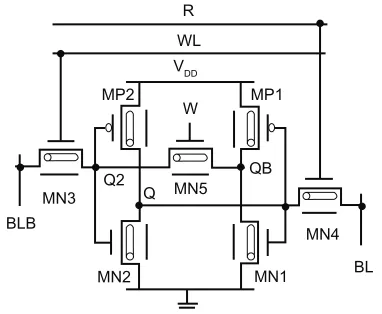
Aly et al28 proposed a CMOS-7T SRAM cell similar to
the proposed CNFET-7T shown in Figure 3 (or Figure 4), basically to reduce the activity factor αBL for
reduc-tion of dynamic power while writing to a cell given by
PWRITE=αBL× CBL× V 2DD× FWRITE, where αBL is the switching
activity factor for writing, CBL is the bitline capacitance, VDD is the supply voltage, and FWRITE is the writing frequency to the SRAM cell. But static power consumption in a SRAM cell is more critical than dynamic power consumption, since whole parts of the cache remains idle most of the time except the row being accessed. Therefore, this paper proposes imple-mentation of 7T SRAM with CNFET operating at OEP and demonstrates that the proposed design is better in terms of standby power dissipation.
read/write operation
Both BL and BLB are precharged high before and after each read/write operation. The write operation in the 7T/CNFET-7T cell starts by turning MN5 off. Complement of data to be written to node Q is applied to BLB and MN3 is turned on by asserting WL high, leaving MN4 off. BL and MN4 do not take part in the write operation. During standby mode, MN3 and MN4 are kept off applying WL and R low, MN5 is kept on asserting W high. During read operation with QB storing “0”, BLB discharges through the critical read path consists of MN3, MN5, and MN1. BL discharges through the read path MN4 and MN2 during read operation with Q storing “0”. Main device and technology parameters for 7T cell used for comparison with the proposed design are tabulated in Table 2. As MN1 $ 3 and MN2 $ 2 ensure stable read operation,28 the transistors in the 7T cell are sized as
shown in Table 2. The 7T also requires low-Vt MN5. To avoid extra masking cost and to fulfill this requirement, the diameter of MN5 is increased to reduce its Vt in the proposed design. Other devices used for the design are square transistors with
0.8
(7,0.78857)
(13, 0.4246) (11, 0.5018)
(36, 0.153) 0.7
0.6
0.5
0.4
0.3
0.2
0.1
0 10 20 30 40
Chirality vector n1
Threshold voltage of N–CNFET (V)
Figure 2 Threshold voltage (Vt) versus chirality vector (n1).
Abbreviation: cNFeT,carbon nanotube field effect transistor.
R WL
MP1 MP2
W VDD
BLB
MN2 MN3
MN1 MN4 MN5
Q2 Q
QB
BL
Figure 3 cNFeT-based 7T SrAM cell.
Abbreviation: CNFET, carbon nanotube field effect transistor; SRAM, static random access memory.
MN3
MN2 MN5 MN1
BL MP2
QB=’1’ VQ=’0’
MP1 WL
R
MN4 W
VDD
Q2
BLB
Subthreshold leakage (Isub) Junction leakage (Ijn) Gate leakage (Igd)
Figure 4 Leakage components in 7T SrAM cell.
Abbreviations: 7T, seven-transistor; SrAM, static random access memory.
Table 2 Device and technology parameters of cMOS-based 7T
Parameter CMOS-based 7T
Vtn0 0.63 V
Vtp0 −0.5808 V
MP1, MP2 W = 22 nm, L = 22 nm
MN1 W = 66 nm, L = 22 nm
MN2 W = 44 nm, L = 22 nm
MN3, MN4, MN5 W = 22 nm, L = 22 nm
Abbreviations: cMOS, complementary metal-oxide semiconductor; 7T, seven-transistor; W, width; L, length.
Nanotechnology, Science and Applications downloaded from https://www.dovepress.com/ by 118.70.13.36 on 24-Aug-2020
Dovepress Power optimized variation aware dual-threshold SrAM cell design technique
minimum channel length. This work implements
CMOS-based 7T SRAM cell using dual-diameter dual-Vt CNFETs,
and its performance is assessed at OEP.
To investigate the performance in terms of various design metrics, extensive simulations are run on HSPICE (high-performance simulation program with integrated circuit emphasis), and finally CNFETs with two different diameters are selected to achieve optimum results. HSPICE has been an industry-standard circuit simulator for the past 30 years with an error of less than 5%. As mentioned earlier, the diameter selected for MN3 and MN5 is 1.03 nm to increase its drive current, as drive current through CNT is proportional to its diameter. This has resulted in reduction of read and write delays, which are shown later. The diameter of the other five transistors is selected to be 0.8719 nm. The values of device diameters, threshold voltages, and the correspond-ing chirality vectors are tabulated in Table 3. As mentioned earlier, single-tube CNFETs are used in this work.
Simulation results and comparisons
We present measurements of various design metrics which are measured during simulation on HSPICE using
experimen-tally validated CNFET model,23 and 22 nm CMOS Berkeley
Predictive Technology Model (BPTM).29 The CNFET model
has been calibrated to 90% accuracy with experimental data (AC and DC characteristics) from fabricated CNFET circuits.30
Standby power
The leakage current is the major contributor to the total power consumption in SRAM cell in nanoscaled technology. The total leakage current in a SRAM cell is mainly (neglect-ing minor components such as IGIDL and Ipunchthrough) due to subthreshold-leakage current (Isub), the gate-leakage current (Igate) and the reverse-biased drain- and source-body junction band-to-band tunneling (BTBT) leakage current (Ijn) through different transistors as shown in Figure 4:31−33
Isub=Isub MN4+Isub MN1+Isub MP2
Ijn =2Ijn MN3+Ijn MN4+Ijn MN1+Ijn MP2+2IJN MN5
I I I I I
I I
gate gd MN gs MN gd MN gd MP
gd MN gs MN
= + + +
+ 3 2+ 3 2+ 4 2
IIgd MP1+Igs MP1+Igd MN1
Ileak =Isub+Ijn+Igate (3)
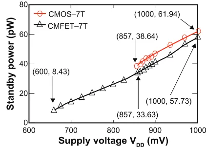
Figure 4 shows the various leakage components in 7T, with storage node Q and QB storing the values as indicated.
The SPWR (standby power) consumed due to these leakage
currents is measured at various voltage points starting from
VDD= 1 V to the minimal voltage of VDD= 857 mV and 660 mV for 7T and CNFET-7T respectively. As the cell is asymmetrical, the measurement is done under two conditions with storage node Q storing “0” and Q storing “1” because it is evident from Figure 4, that the leakage components, and thus the current equation differ depending on stored value at Q and QB.
The measured results are averaged and the mean values are plotted in Figure 5, where important measurement points are marked with arrows. Compared with 7T (operating at
VDD= 1 V consuming 61.94 pW), the CNFET-7T (operating
at 1V consuming 57.73 pW) saves 1.073× standby power.
As observed from Figure 5, the 7T consumes 38.54 pW whereas CNFET-7T consumes 33.63 pW at iso-operating voltage of 857 mV. Therefore even if the proposed design is operated at the minimum operating voltage of 7T (ie, VDD= 857 mV) there is a saving in SPWR by 1.146×. This is attributed to the higher leakage current components in MOSFET compared with CNFET. That is, OFF-current of CNFET is much lower than that of MOSFET. As illustrated in Figure 5, if the CNFET-7T is operated at 660 mV, there will be a substantial amount of saving in SPWR.
Under the measuring condition used (with equal wordline slew rate and on time), 7T could be operated up to 857 mV and CNFET-7T could be operated up to 660 mV without
Table 3 Device parameters of proposed design
CNFETs Chirality
vector
Threshold voltage (V)
Diameter (nm)
MP1, MP2, MN1, MN2, MN4
(11, 0) |0.5018| 0.8719
MN3, MN5 (13, 0) 0.4246 1.03
Abbreviation: CNFET, carbon nanotube field effect transistor.
80
60
40
20
0
600 700 (600, 8.43)
(857, 33.63)
(1000, 57.73) (1000, 61.94)
(857, 38.64)
800 900 1000
Supply voltage VDD (mV)
Standby power (pW
) CMOS–7T
CMFET–7T
Figure 5 Standby power (SPWr) measured with Q storing “0”.
Abbreviations: cMOS,complementary metal-oxide semiconductor; cNFeT, carbon nanotube field effect transistor.
Nanotechnology, Science and Applications downloaded from https://www.dovepress.com/ by 118.70.13.36 on 24-Aug-2020
Dovepress
Islam and Hasan
facing read and write failure. If the measuring condition is changed, both the design can be operated even in the near subthreshold region. Particularly, CNFET-7T can be oper-ated in subthreshold region without failure. However, the designs are operated in the superthreshold region to explore OEP in this region without compromising much with delay penalty. The iso-operating voltage, ie, 857 mV, is found to be OEP, without incurring much delay in accessing the cell. VDD can be further scaled down for CNFET-7T for improved results.
read/write access time
Figure 6 shows the read access time (TRA) versus VDD plot. The TRA is estimated as the time required for developing a voltage differential to be sensed by the sense amplifier (not shown) from the point when WL reaches 50% of its full swing from its initial low level to the point when BL/BLB falls by 10% of its full swing from its initial high value. As the cell is asymmetrical, the measurement is done under two conditions – with storage node Q storing “0” and Q storing “1” and the results are averaged before plotting. It is observed from Figure 6 that the read delay of 7T at iso-operating
voltage of 857 mV is 1.321× compared with CNFET-7T.
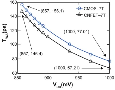
Figure 7 shows the write access time (TWA) versus VDD
plot. While writing “0” to Q, BLB is raised high and the write operation is completed after two inverter delays when QB settles to its new state. Therefore, this operation takes quite a long time compared with the read operation. MN3 of CNFET-7T is of low-Vt. Therefore, it passes a higher voltage to the gate of MN2 driving it harder (compared with 7T) both in cases of reading as well as writing, thereby reducing the
read/write delay. The CNFET-7T offers 1.066× improvement
in write delay at iso-operating voltage of VDD= 857 mV. As observed from Figures 5 and 6, operation of CNFET-7T
at OEP instead of VDD= 1 V offers 41.7% improvement in
SPWR incurring 44.5% penalty in TRA, whereas operation of
7T at OEP instead of VDD= 1V offers 37.8% improvement in
SPWR incurring 53.5% penalty in TRA. Therefore, the proposed design is superior to its CMOS counterpart in terms of most of its major design metrics discussed so far.
Write access time variation
We present variation measurements of write-access time (TWA), which is measured during simulation on HSPICE. Monte Carlo simulations are performed for the measurements. Monte Carlo simulation is a method for iteratively evaluat-ing a design. The goal is to determine how random variation on process parameters, voltage, and temperature affects the performance and reliability of a design. The standard devia-tion (σ) is a measure of dispersion (or variability) that states numerically the extent to which individual observations vary on average. Figure 8 plots the normalized standard devia-tion of TWA of the two designs at OEP (VDD= 0.857 V) and
VDD= 1V. It is observed from the figure that the proposed design shows 1.4× less variation in write access time at
0.857 V and 1.2× at 1 V. This shows the robustness of the
850 60
50
40
30
20
900 950 1000
VDD (mV)
(1000, 25.99)
(1000, 23.51) (857, 55.92)
(857, 42.34)
CMOS–7T CNFET–7T
TRA
(ps)
Figure 6 read access time versus VDD.
Abbreviations: cMOS,complementary metal-oxide semiconductor; cNFeT, carbon nanotube field effect transistor.
CMOS–7T CNFET–7T 160
140
120
100
80
60
850 900 950 1000
(1000, 67.21) (1000, 77.01) (857, 156.1)
(857, 146.4)
VDD(mV) TWA
(ps)
Figure 7 Write access time versus VDD.
Abbreviations: cMOS, complementary metal-oxide semiconductor; cNFeT, carbon nanotube field effect transistor.
1.5
0.5
0
0.857V 1.4X
1.2X
1V 1
Normalized
σ
of
TWA CNFET–7T
CMOS–7T
Figure 8 Write delay variation measurement.
Abbreviations: cMOS, complementary metal-oxide semiconductor; cNFeT, carbon nanotube field effect transistor.
Nanotechnology, Science and Applications downloaded from https://www.dovepress.com/ by 118.70.13.36 on 24-Aug-2020
Dovepress Power optimized variation aware dual-threshold SrAM cell design technique
proposed design against PVT variations. Ideally ID is supposed to be constant in saturation region. However, in practice, increasing VDS (drain-to-source voltage) beyond VDS-sat (drain- to-source saturation voltage) does affect the chan-nel somewhat. As the VDS is increased, the depletion layer widens, thereby reducing the effective channel length. Since
ID is inversely proportional to the channel length, ID increases with VDS. This DIBL (drain-induced barrier lowering) or SCE (short-channel effect) is more pronounced in small geometry MOSFET, and it has negligible impact on CNFET, which is evident from Figure 1. It clearly shows that the ID in saturation region is almost constant in case of CNFET, whereas it shows almost linear increase in case of MOSFET. This signifies the variation in ID with VDS. It is needless to say that during read/write operations node voltages change thereby varying
VDS and finally causing variation in TWA and TRA.
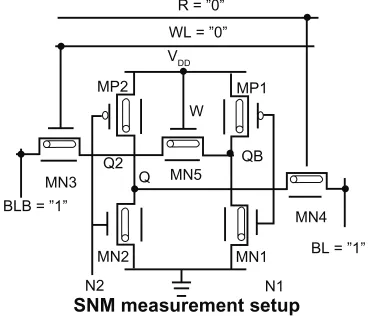
Static noise margin measurements
The static noise margin (SNM) of SRAM cell is defined as the minimum DC noise voltage necessary to flip the state of the cell. SNM of an SRAM is a widely used design metric that measures the cell stability. Simulation measurement of SNM is carried out for both the designs. Figure 9 shows a test setup for measuring SNM. Figure 10 plots the combined “butterfly curve” of 7T and proposed CNFET-7T at OEP (iso-operating voltage of VDD= 857 mV). The butterfly curve is obtained in the following way using the test circuit: 1) W and bit lines (BL, BLB) are biased at VDD and WL and R is biased at ground;
2) Voltage of N1 is swept from 0 V to VDD while measuring
voltage of QB; 3) Voltage of N2 is swept from 0 V to VDD while measuring voltage of Q in the same way; and 4) Measured voltages are plotted to get a butterfly curve. The side length of maximum square that can be embedded within the smaller lobe of the butterfly curve represents the SNM of the cell.
This definition holds good because, when the value of noise voltage increases from 0, the VTC (voltage transfer characteristic) for inverter 1 formed with MP1 and
MN1 moves to the right and the VTC−1 (inverse VTC) for
inverter 2 formed with MP2 and MN2 moves downward. Once they both move by the SNM value, the curves meet at only two points and any further noise flips the cell.34
As observed from Figure 10, the SNM of 7T is 160 mV, whereas that of CNFET-7T is 250 mV, showing 56.3% improvements in CNFET-7T over the 7T cell. To understand why this happens, remember that both the transistors MN1
and MN2 of CNFET-7T have lower Vt, which implies that
the switching threshold of both the inverters are lower than that of 7T. This shifts the VTC of inverter 1 to the left and pushes the VTC−1 of inverter 2 down making both the lobes
of the butterfly curve wider.
R = ”0” WL = ”0”
MP1 MP2
W VDD
BLB = ”1”
MN2
N2 MN3
MN1
N1 MN4 MN5
Q2 Q
QB
BL = ”1”
SNM measurement setup
Figure 9 Test setup for measuring static noise margin (SNM).
solid sqr: 7T SNM = 160 mV
SNM = 250 mV dashed sqr:
CNFET–7T
QB (Volts
)
0 0.2 0.4 0.6 0.8 1
0 0.2 0.4 0.6 0.8 1
CMOS–7T CNFET–7T
Figure 10 SNM of 7T and cNFeT-7T.
Abbreviations: cMOS, complementary metal-oxide semiconductor; cNFeT, carbon nanotube field effect transistor; SNM, static noise margin.
R WL
MP1 MP2
W VDD
BLB = ”1”
MN2
N2 N1
MN3
MN1 MN4 MN5
Q2 Q QB
BL = ”1”
RSNM measurment setup
Figure 11 Test setup for measuring read static noise margin (rSNM).
Nanotechnology, Science and Applications downloaded from https://www.dovepress.com/ by 118.70.13.36 on 24-Aug-2020
Dovepress
Islam and Hasan
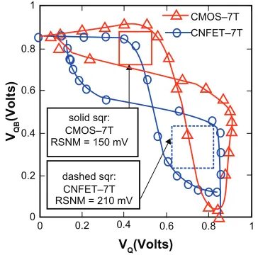
read static noise margin measurements
The SRAM cell is the most susceptible to noise during read operation since the node storing “0” (say, Q in Figure 4) rises to a voltage higher than ground due to a voltage dividing effect between the access transistor (say, MN4) and inverter pull-down NMOS driver (say, MN2). The ratio of the widths of the pull-down transistor to the access transistor, com-monly referred to as the cell ratio (CR) or β ratio, decides how high the “0” storage node rises during a read operation. Smaller CRs translate into a larger voltage drop across the pull-down transistor, requiring a smaller noise voltage at the node storing “0” to trip the cell. RSNM is a measure of how much noise voltage is required at the node storing “0” to flip the state of an SRAM cell while reading. Therefore, RSNM is an even more critical design metric of the SRAM cell than SNM. Figure 11 shows a test setup for measuring RSNM. The butterfly curves are obtained with this test setup and using the same measuring technique as done for SNM. Figure 12 plots the combined butterfly curve of 7T and CNFET-7T at OEP. The plot shows that the CNFET-7T outperforms 7T by 40% improvement in RSNM. The reason is obvious from the discussion in the preceding subsection.
Conclusion
We propose a dual-Vt CNFET-based low-power PVT varia-tion immune 7T SRAM cell. We observe during the inves-tigation that the CNFET-based 7T SRAM cell offers better performance in terms of most the design parameters such as standby power and noise margins. The proposed design also shows more robustness against process variations compared with the CMOS-based 7T SRAM cell. This is due to proper
selection of CNFET diameter and hence threshold voltage for appropriate transistors. This is also due to the cylindrical geometry of CNFET. A variation in the gate oxide thickness that strongly affects the drive current and capacitance of CMOS transistors has a negligible impact on the CNFET’s operation. We have successfully demonstrated that the proposed design will be effective to reduce standby power, read/write delay, and write delay variation.
Disclosure
The authors report no conflicts of interest in this work.
References
1. Zhang K, Bhattacharya U, Chen Z, et al. A 3-GHz 70-Mb SRAM in 65-nm CMOS technology with integrated column-based dynamic power supply. IEEE J Solid-State Circuits. 2006;41(1):146–151.
2. Nii K, Yabuuchi M, Tsukamoto Y, et al. A 45-nm bulk CMOS embed-ded SRAM with improved immunity against process and temperature variations. IEEE J Solid-State Circuits. 2008;43(1):180–191. 3. Ohbayashi S, Yabuuchi M, Nii K, et al. A 65-nm SoC embedded
6T-SRAM designed for manufacturability with read and write operation stabilizing circuits. IEEE J Solid-State Circuits. 2007; 42(4):820–829.
4. Burnett D, Erington K, Subramanian C, Baker K. Implications of fundamental threshold voltage variations for high-density SRAM and logic circuits. Proceedings of the Symposium onVLSI Technology; Honolulu, HI: IEEE; 1994 Jun 7–9:15–16.
5. Seevinck E, List F, Lohstroh J. Static-noise margin analysis of MOS SRAM cells. IEEE J Solid-State Circuits. 1987;SC-22:748–754. 6. Tschanz JW, et al. Adaptive body bias for reducing impacts of
die- to-die and within-die parameter variations on microprocessor frequency and leakage. IEEE J Solid-State Circuits. 2002;37(11): 1396–1402.
7. Borkar S. Design challenges of technology scaling. IEEE Micro. 1999;19(4):23–29.
8. Semiconductor Industry Association (SIA), International Technology Roadmap for Semiconductors 2005 Edition. Available from: http:// www.itrs.net/Links/2005ITRS/Home2005.htm. Accessed January 13, 2011.
9. Markovic D, Wang CC, Alarcon LP, Liu TT, Rabaey JM. Ultralow-power design in near-threshold region. Proc IEEE; 2010;98(2): 237–252.
10. Deng J. Device modeling and circuit performance evaluation for nanoscale devices: silicon technology beyond 45 nm node and carbon nanotube field effect transistors. Ph.D. dissertation. Stanford, CA: Stanford University Press; 2007.
11. Patil N, Lin A, Zhang J, et al. Scalable carbon nanotube computational and storage circuits immune to metallic and mis-positioned carbon nanotubes. IEEE Trans Nanotechnol. 2010;(99).
12. Patil N, Lin A, Myers ER, Wong HSP, Mitra S. Integrated wafer-scale growth and transfer of directional carbon nanotubes and misaligned-carbon-nanotube-immune logic structures. Proc Symp VLSI Technology Digest Tech Papers. 2008;205–206.
13. Patil N, Deng J, Lin A, Wong HSP, Mitra S. Design methods for mis-aligned and mis-positioned carbon-nanotube-immune circuits. IEEE Trans Comput Aided Des Integr Syst. 2008;27(10):1725–1736. 14. Patil N, Lin A, Myers E, et al. Wafer-scale growth and transfer of
aligned single-walled carbon nanotubes. IEEE Trans Nanotechnol. 2009;8(4):498–504.
15. Kang SJ, Kocabas C, Ozel T, et al. High-performance electronics using dense, perfectly aligned arrays of single-walled carbon nanotubes. Nat Nanotechnol. 2007;2:230–236.
RSNM = 150 mV
RSNM = 210 mV dashed sqr: CNFET–7T solid sqr: CMOS–7T VQB
(Volts)
VQ(Volts) 0
0.2 0.4 0.6 0.8 1
0 0.2 0.4 0.6 0.8 1
CMOS–7T CNFET–7T
Figure 12 read static noise margin (rSNM) of 7T and cNFeT-7T.
Abbreviations: cMOS, complementary metal-oxide semiconductor; cNFeT, carbon nanotube field effect transistor.
Nanotechnology, Science and Applications downloaded from https://www.dovepress.com/ by 118.70.13.36 on 24-Aug-2020
Nanotechnology, Science and Applications
Publish your work in this journal
Submit your manuscript here: http://www.dovepress.com/nanotechnology-science-and-applications-journal Nanotechnology, Science and Applications is an international,
peer-reviewed, open access journal that focuses on the science of nanotech-nology in a wide range of industrial and academic applications. It is characterized by the rapid reporting across all sectors, including engi-neering, optics, bio-medicine, cosmetics, textiles, resource sustainability
and science. Applied research into materials, particles, nano-structures and fabrication, diagnostics and analytics, drug delivery and toxicology constitute the primary direction of the journal. The manuscript management system is completely online and includes a very quick and fair peer-review system, which is all easy to use.
Dovepress
Dove
press
Power optimized variation aware dual-threshold SrAM cell design technique 16. Deng J, Patil N, Ryu K, et al. Carbon nanotube transistor circuits:
circuit-level performance benchmarking and design options for living with imperfections. Proc International Solid State Circuits Conference (ISSCC). 2007:70–71.
17. Patil N, et al. Circuit-level performance benchmarking and scalability of carbon nanotube transistor circuits. IEEE Trans Nanotechnol. 2009;8(1):37–45.
18. Akinwande D, et al. Monolithic integration of CMOS VLSI and carbon nanotubes for hybrid nanotechnology application. IEEE Trans Nanotechnol. 2008;7(5):636–639.
19. Javey A, Guo J, Farmer DB, et al. Self-aligned ballistic molecular tran-sistors and electrically parallel nanotube arrays. Nano Lett. 2004;4(7): 1319–1322.
20. Yao Z, Kane CL, Dekker C. High-field electrical transport in single-wall carbon nanotubes. Phys Rev Lett. 2000;84(13):2941–2944.
21. Mann D, Javey A, Kong J, Wang Q, Dai H. Ballistic transport in metal-lic nanotubes with reliable Pd ohmic contacts. Nano Lett. 2003;3(11): 1541–1544.
22. Cui Y, Zhong Z, Wang D, Wang WU, Lieber CM. High performance sil-icon nanowire field effect transistors. Nano Lett. 2003;3(2):149–152. 23. Stanford University CNFET Model Web site. 2008. Available from:
http://nano.stanford.edu/model.php?id=23. Accessed January 13, 2011. 24. Mintmire JW, White CT. Universal density of states for carbon
nanotubes. Phys Rev Lett. 1998;81(12):2506–2509.
25. Deng J, Wong HSP. A compact SPICE model for carbon-nanotube field-effect transistors including nonidealities and its application – part I: model of the intrinsic channel region. IEEE Trans Electron Devices. 2007;54(12):3186–3194.
26. Deng J, Wong HSP. A compact SPICE model for carbon-nanotube field-effect transistors including nonidealities and its application – part II: full device model and circuit performance benchmarking. IEEE Trans Electron Devices. 2007;54(12):3195–3205.
27. Lin S, Kim YB, Lombardi F. CNFET-based SRAM cell by dual-chirality selection. IEEE Trans Nanotechnol. 2010;9(1):30–37.
28. Aly R, Faisal M, Bayoumi A. Novel 7T SRAM cell for low power cache design. Proc IEEE International SOC Conf. IEEE; 2005 Sep: 171–174.
29. Berkeley Predictive Technology Model (PBTM). Available from: http:// www-device.eecs.berkeley.edu/∼ptm/. Accessed January 13, 2011. 30. Amlani I, Lewis J, Lee K, et al. First demonstration of AC gain from
a single-walled carbon nanotube common-source amplifier. Proc Int Electron Devices Meet. 2006:1–4.
31. Roy K, Mukhopadhyay S, Mahmoodi-Meimand H. Leakage current mechanisms and leakage reduction techniques in deep-submicrometer CMOS circuits. Proc IEEE; 2003;91(2):305–327.
32. Mukhopadhyay S, Raychoudhury A, Roy K. Accurate estimation of total leakage current in scaled CMOS logic circuits based on compact current modeling. Proc 40th Annual Design Automation Conference (DAC). Anahiem, CA: ACM; 2003 Jun 2–6:169–174.
33. BSIM4.2.1 MOSFET Model, BSIM Group, UC Berkeley. Avalil-able from: http://www-device.eecs.berkeley.edu/bsim3/. Accessed January 13, 2011.
34. Calhoun BH, Chandrakasan AP. Static noise margin variation for sub-threshold SRAM in 65-nm CMOS. IEEE J Solid-State Circuits. 2006;41(7):1673–1679.
Nanotechnology, Science and Applications downloaded from https://www.dovepress.com/ by 118.70.13.36 on 24-Aug-2020