Wideband High Gain Antenna Subarray for 5G Applications
Seyyedehelnaz Ershadi1, *, Asghar Keshtkar1, Ahmed H. Abdelrahman2, and Hao Xin3
Abstract—Wideband arrays have recently received considerable attention in 5G applications to cover larger frequency bands. This paper presents a novel design of a high gain and wideband antenna subarray from 23 GHz to 32 GHz, which covers the frequency bands proposed by the Federal Communications Commission (FCC) for 5G communications. The proposed subarray consists of four radiating elements with wideband and high gain characteristics. These elements are composed of two stacked patches, which are fed using the proximity coupling technique. A unit-cell element prototype is first fabricated and tested to validate the gain and bandwidth performances. A 1×4 subarray prototype is then fabricated and tested, while maintaining an element spacing less than half-wavelength at the center frequency, to avoid grating lobes and to keep the small size of the antenna subarray. The measurement results of the prototypes, i.e., unit cell element and subarray prototypes, show good agreements with the simulations. The subarray measurements demonstrate a high gain of 10–12 dBi, an impedance bandwidth of 33.4%, and a 1-dB gain bandwidth of 10.5%. The proposed antenna subarray is a good candidate for wideband and high gain antenna arrays suitable for 5G mmW applications.
1. INTRODUCTION
The next generation of mobile systems (5G) will achieve a quantum leap in communication technology in terms of channel capacity and data throughput. Consequently, the global trend seeks to transfer the operation of mobile systems to the millimeter wave (mmW) band. Antenna arrays, usually organized by subarrays, are good candidates for the mmW band to compensate for the high path loss in that band in exchange for design complexity and system cost. Several key international mobile network operators and academic institutions have started to look into the technological developments toward the next cellular generation, i.e., the fifth generation (5G). In [1–4], the suitability of different millimeter wave (mmW) frequencies and their propagation characteristics are discussed. Extensive propagation measurements presented in [5, 6] demonstrate that mmW systems can offer less interference and more capacity compared to the fourth generation (4G) cellular networks. Additionally, the non-line-of-sight (NLOS) outdoor coverage is possible up to 200 m from a low-power base station. Channel measurements that carried out in [7–9] indicate that mmW propagation is quite viable with directional, high gain antennas. Different path loss and channel models, as well as outage probabilities, signal-processing algorithms and quality of service aware schemes are provided in [10–17] for 5G system simulations and designs in mmW band.
As reviewed, the representatives of industry and academia have proposed the utilization of mmW spectrum to increase the available capacities and data rates while significantly reduce the latency and size of components. Two mmW Gbps Broadband (MGB) candidates, considered by the Federal Communications Commission (FCC) for next generation Mobile Radio Services, are between 24 GHz and 32 GHz, which includes 24.25 GHz–24.45 GHz, 25.05 GHz–25.25 GHz and the Local Multipoint
Received 13 June 2017, Accepted 29 August 2017, Scheduled 15 September 2017 * Corresponding author: Seyyedehelnaz Ershadi ([email protected]).
Distribution Service (LMDS) frequency bands operating at frequencies 27.5 GHz–28.35 GHz, 29.1 GHz– 29.25 GHz, and 31 GHz–31.3 GHz [18]. However, sensitivity to blockage, propagation losses, shadowing, large-scale attenuation of materials and human bodies, and atmospheric absorption are the main challenges in using these frequencies. To overcome these challenges, highly directional antennas should be deployed. Antenna array of multiple elements focuses the radio energy into a narrow beam with high gain, which enhances the effective isotropic radiated power (EIRP) without increasing the transmitter power [19].
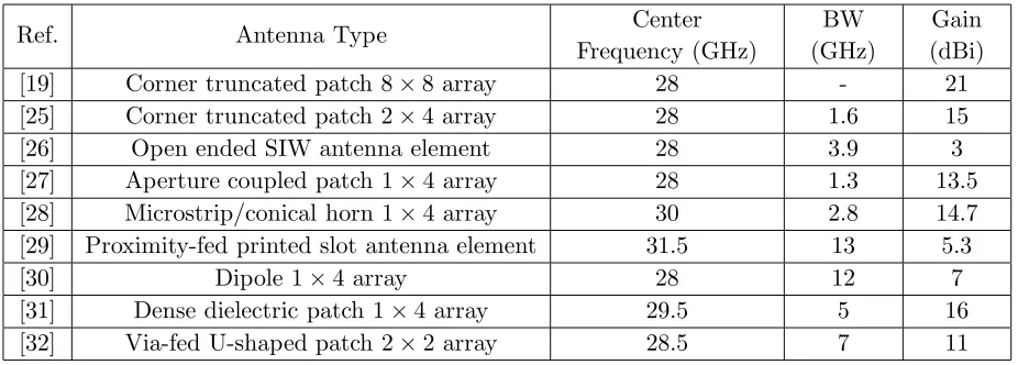
While microstrip antennas have been the subject of many intensive works for decades [20–24], they have been considered in some research efforts reported in the past few years on antenna design aspect of the newly emerging mmW wireless communications [19, 25–32]. Antennas in [19] and [25–28] are mainly designed to operate in one of the target frequency bands, as listed in Table 1. Nevertheless, wideband antenna arrays have received interests in 5G applications as they cover larger frequency bands and provide wider bandwidth and higher data rates. One popular strategy in designing wideband antenna arrays, while maintaining simplicity in development of the beamforming network (BFN), is to use repeating wideband subarrays as the building blocks. In [29], a wideband proximity-fed printed slot antenna element is proposed. The element has a wide bandwidth of 13 GHz, centered at 31.5 GHz, but the maximum achievable gain is only 5.3 dBi. In [30], Samsung Telecommunications proposed a 4-element beam steering capable dipole array with a bandwidth of 12 GHz, centered at 28 GHz, with a moderate maximum gain of 7 dBi. In [31], a four-element dense dielectric (DD) patch array antenna was introduced in which electromagnetic bandgap (EBG) structure and a dielectric superstrate were used to improve the radiation characteristics. This array provided a bandwidth of 5 GHz and a maximum gain of 16 dBi, but the element spacing is larger than one wavelength, i.e., 12 mm, at the center frequency. In [32], Huawei Technologies presented a LMDS 2×2 broadband antenna array composed of unique via-fed U-shaped patch elements, separated by about 0.6 wavelength at 27 GHz, and a stripline distribution network. It provided a 7 GHz bandwidth and a maximum gain of 11 dBi. Table 1 summarizes the results of some published mmW antenna designs.
Table 1. Summarized results of published mmW antennas.
Ref. Antenna Type Center
Frequency (GHz)
BW (GHz)
Gain (dBi) [19] Corner truncated patch 8×8 array 28 - 21 [25] Corner truncated patch 2×4 array 28 1.6 15
[26] Open ended SIW antenna element 28 3.9 3
[27] Aperture coupled patch 1×4 array 28 1.3 13.5 [28] Microstrip/conical horn 1×4 array 30 2.8 14.7 [29] Proximity-fed printed slot antenna element 31.5 13 5.3
[30] Dipole 1×4 array 28 12 7
[31] Dense dielectric patch 1×4 array 29.5 5 16 [32] Via-fed U-shaped patch 2×2 array 28.5 7 11
that the proposed subarray is a good candidate for the design of large 5G antenna arrays to compensate for the high path loss of mmW propagation. This can be achieved through the adaptive beam control technology, which applies high gain and narrow beams that increase the directional signal to noise ratio (SNR).
2. UNIT CELL ELEMENT DESIGN
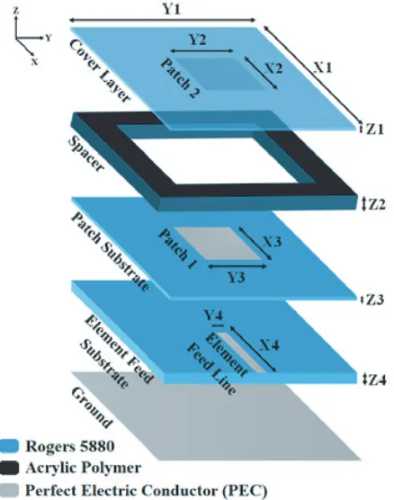
Stacking of multiple patches is a technique used to realize multiple resonances, hence improve the antenna bandwidth, while maintaining the same surface area occupied by the antenna. Moreover, the radiation pattern of the stacked element is stable over the operation bandwidth. These considerations are important in array applications to obtain wideband performance without introducing grating lobes. Figure 1 presents the structure of the unit-cell element. It composed of four dielectric layer; a cover layer, a spacer, a patch substrate, and an element feed substrate. Patch 1 is the driven patch and patch 2 is a parasitic patch. Both are aligned at their centers to avoid beam squint in the E-plane. Patch 1 is fed using the proximity coupling technique to enhance the bandwidth and the radiated power, and to reduce the conductor loss [33–35]. Proximity coupling fed is also preferable, compared with the coaxial fed technique, to reduce the fabrication complexity and improve the mechanical strength of the structure. Patch 2 has the advantage of adding another resonance to the main resonance of patch 1 and thereby increasing the bandwidth. The cover layer is a thin dielectric superstrate located on the top of patch 2 aiming to protect it from the environment, as well as it improves the gain of the multilayered structure.
Figure 1. Structure of the proposed unit-cell element.
periphery and thus improves the radiated power. Accordingly, the element feed and patch substrates are chosen to be Rogers 5880 with εr = 2.2 and tanδ = 0.0009. This high frequency laminate has a
constant relative permittivity over a wide frequency range, and its low dissipation factor extends its usefulness in the mmW band.
The initial values of the width (W) and length (L) of a patch can be calculated using the well-known equations in [37]. Using these equations, we calculated the dimensions (L×W) of the patches 1 and 2, which are equal to 3.2 mm×3.8 mm (X3×Y3) and 3.4 mm×4.5 mm (X2×Y2), respectively. Usually the patch width W has minor effect on the resonant frequency and the radiation pattern. However, extensive reduction in the patch width reduces the radiation efficiency. As we aim to reduce the element dimensions and also keep the high radiation efficiency, we calculated the lower bound of the patch width (Wmin in mm) using (1) [38]:
Wmin=
144π fmin −L
2π (1)
wherefmin(in GHz) is the minimum operating frequency under consideration. For a minimum operating frequency of 24 GHz, the minimum width of both patches 1 and 2 is about 2.5 mm. We have used the calculated minimum patch width as a starting value for the optimization process of the unit cell element. For a characteristic impedance of 50 Ω and a substrate thickness of 0.381 mm, the initial value of the feed line width was calculated equal to 1.22 mm.
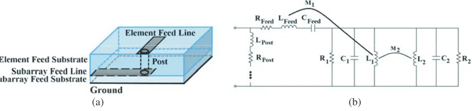
The equivalent circuit of the unit cell element is shown in Fig. 2. The intrinsic behavior of each patch is represented by a RLC resonator. The coupling between the two patches is the mutual inductance,M2, that occurred between the two inductors. Coupling between patch 1 and the feed line is capacitive in nature [39] and is represented byCF eed. This capacitance composed of a capacitance (C) that occurred
between patch 1 and the feed line, and a capacitance (Cf) that is equivalent to the fringing effect of the
feed line. Capacitance C is directly proportional to the area that represents the mapping of the patch on the feed line (a) and inversely proportional to the patch substrate thickness (h), such that:
C=ε0εra
h (2)
Figure 2. The equivalent circuit of the proposed unit-cell element.
(a) (b)
whereε0 and εr are the permittivity of free space and the relative permittivity of the patch substrate,
respectively. The capacitance (Cf) can be calculated as [40]:
Cf = le
cZ0
√ εreff
(3)
wherele is the increment in the feed line due to the fringing fields. CF eed can then be calculated as:
CF eed=CCf. (4)
Using Eqs. (2)–(4), we calculate CF eed equal to 0.089 pF at 31.1 GHz, which imposes a capacitive
reactance of 57.6 Ω for the input impedance of patch 1. To avoid the side effects of the coaxial connection during the pattern measurements, we have extended the feed line, as shown in Fig. 3(a). This feed-line extension is well represented by an inductor, LF eed in series with a resistor, RF eed [41]. The coupling
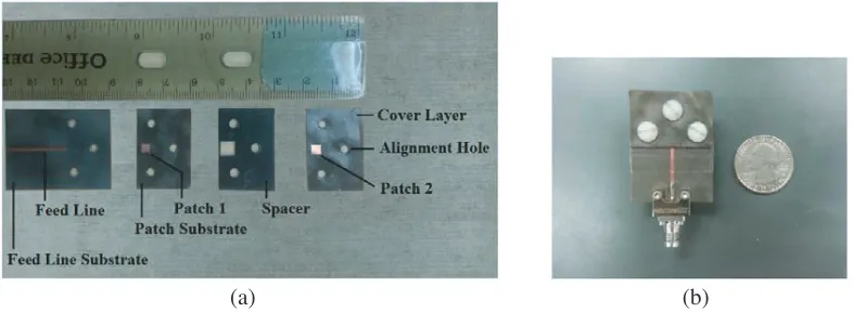
betweenL1 and LF eed is also considered asM1. The element values of the equivalent circuit are listed in Table 2. The proposed unit cell element was then simulated using HFSS simulation software. The dimensions of the patches, the spacer thickness and the feed line width were optimized for wideband coverage and gain maximization. The optimized dimensions are listed in Table 3 [42]. Fig. 3(a) shows the prototype of the proposed unit cell element, which was fabricated using the photolithography process. A 2.4 mm SMK connector is used, which operates up to 50 GHz. Three nylon screws are used to align the stacked layers.
Table 2. Element values for the equivalent circuit of the simulated unit cell.
Element Value (Ω) Element Value (nH) Element Value (pF)
R1 260 L1 0.0156 C1 1.8182
R2 5901 L2 0.367 C2 0.06938
RFeed 47.92 LFeed 0.3097 CFeed 0.0898
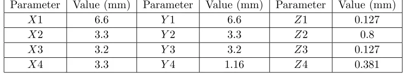
Table 3. Dimensions of the proposed unit cell element.
Parameter Value (mm) Parameter Value (mm) Parameter Value (mm)
X1 6.6 Y1 6.6 Z1 0.127
X2 3.3 Y2 3.3 Z2 0.8
X3 3.2 Y3 3.2 Z3 0.127
X4 3.3 Y4 1.16 Z4 0.381
Figure 4(a) compares the reflection coefficient results of the full-wave simulation, the equivalent circuit model simulation, and the measurements. Impedance bandwidths of 29.5% (25.4–34.2 GHz) and 34.2% (24–33.9 GHz) are obtained for the simulation and measurements, respectively. We can notice three resonances at 28.4 GHz, 31.1 GHz and 33.4 GHz. The two higher resonances are created due to the edge currents flow around the exteriors of the two patches, and when their lengths are equal to half of the effective wavelength. The lowest resonance is due to the coupling between the two patches, which enhances the current flow and thereby increases the effective wavelength. The simulated and measured gains, illustrated in Fig. 4(b), range between 6–8.7 dB and 5.1–7.9 dB, respectively, over the −10 dB reflection coefficient band. The 1-dB gain bandwidth is measured equal to 12%.
Figure 5 presents the far-field radiation patterns of the unit-cell element at the center frequencies of the bands recommended by the FCC, i.e., 25.1 GHz, 27.9 GHz, 29.2 GHz and 31.1 GHz. The measured cross-polarized levels are less than −21, −19.5, −21 and −20 dB in the E-plane and less than −19.4,
(a) (b)
Figure 4. Simulation and measurement results of the unit-cell element, (a) reflection coefficient and (b) gain.
(a) (b) (c) (d)
Figure 5. Simulated and measured far-field radiation patterns of the unit-cell element, (a) 25.1 GHz, (b) 27.9 GHz, (c) 29.2 GHz, (d) 31.1 GHz.
3. SUBARRAY DESIGN
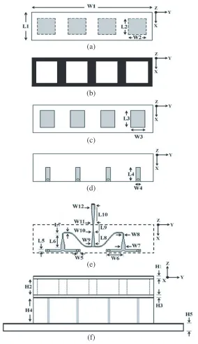
Based on the proposed unit cell element, an antenna subarray is designed, as shown in Fig. 6. The element spacing is optimized, which is a tradeoff between a large enough spacing to reduce mutual coupling between elements and hence larger directive gain and better impedance matching, and a small enough spacing for wider pattern bandwidth and avoiding grating lobes. The upper limit of element spacing (d) to prevent the appearance of grating lobes is calculated as [43]:
d= λreff
(a)
(b)
(c)
(d)
(e)
(f)
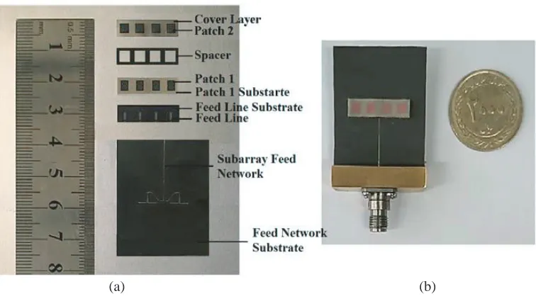
Figure 6. Proposed antenna subarray, (a) cover layer and parasitic patches on its underside, (b) spacer, (c) driven patches layer, (d) patches feed lines, (e) subarray feed network, and (f) side view of the overall subarray structure.
whereλreff is the effective wavelength and θis the look angle, which is usually considered around 25◦– 30◦ in the 5G base stations to provide adequate throughput by spatial multiplexing and minimizing the interference. The element spacing upper limitdwas calculated to be 5.4 mm (look angle of θ= 25◦ and operating frequency of 32 GHz).
Considering an average unit cell element gain of 6 dBi over the bandwidth under consideration, as mentioned in Section 2, a 1×4 antenna subarray can achieve an average gain of 12 dBi based on the proposed proximity coupled staked patch elements.
Table 4. Simulation and measurement results of the unit-cell element.
Parameter Simulations Measurements
Frequency Range (GHz) 25.4–34.2 24–33.9
Impedance Bandwidth 29.5% 34.2%
Gain Range (dB) 6–8.7 5.1–7.9
1-dB gain bandwidth 9.6% 12%
Frequency (GHz) 25.1 27.9 29.2 31.1 25.1 27.9 29.2 31.1
Gain (dB) 6.7 7.9 8.7 6.9 5.2 7.4 7.8 6.8
E-plane cross-pol level (dB) −47.8 −45.9 −46.3 −42.1 −21 −19.5 −21 −20
H-plane cross-pol level (dB) −23 −24.2 −25.6 −23 −19.4 −20.3 −20.1 −20.9
E-plane HPBW (degrees) 86 100 105 108 90 100 102 101
H-plane HPBW (degrees) 50 53 61 64 48 51 56 58 Front to back ratio (dB) −43.1 −28.4 −23.7 −22.6 −33.3 −21.6 −21.3 −30.6
impedance of each element. One solution to compensate for these extra capacitances is to add an inductive section to the design. This is in addition to the need to connect the element feed lines to the subarray feed network which is located on the bottom of the element feed substrate. Accordingly, a post is added, as shown in Fig. 7(a), which is intrinsically an inductive element. A series inductance, i.e.,
LP ost, equivalent to the post, is added to each subarray element, as shown in Fig. 7(b). An approximate
value of the post inductance can be calculated as [39]:
LP ost(nH) = 0.2hP
ln4hP
dP
+ dP
2hP −
1
(6)
where hp is the post height and dp the post diameter, both in millimeter. Considering the minimum
realizable post diameter, i.e., 0.4 mm, a 0.99 mm post height can compensate for the extra feed capacitance. The designed post has a very low DC resistance of 0.0001282 ohms and it imposes a reactance of 60.2 ohms to the input impedance of the structure at 31.1 GHz. This inductive reactance approximately compensates for the capacitance of CF eed. Among available thicknesses of Rogers
substrate RT/Duroid 5880, the one with a thickness of 1.016 mm was selected as the element feed substrate, which is also thick enough to avoid mutual coupling between the subarray feed network and the patches. Accordingly, the width of the element feed line is retuned to compensate for the change in the substrate thickness in comparison with that of the unit cell element. The subarray feed network is then mounted on another RT/Duroid 5880 substrate below the element feed substrate, as shown in Fig. 6.
A corporate subarray feed configuration is designed, as shown in Fig. 8. It is composed of broadband Klopfenstein impedance transformers along with two broadband power dividers with identical path
(a) (b)
Figure 8. Feed network of the proposed antenna subarray.
length to insure uniform amplitude and coherent phase between the subarray elements for broadside beam direction [44]. The curvy transmission lines in the feed network facilitate flexible choice of the element spacing. For measurement purpose, the feed line is extended to avoid side effects of the coaxial connection. A 2.4 mm SMK connector is used for measurements. The four microstrip Klopfenstein impedance transformers gradually match different line impedances, according to Eq. (7), so that the reflected waves are reduced and a maximum power is transferred to the subarray elements [45]:
lnZ(z) = 1
2ln (ZLZ0) + Γ0 coshAA
2
φ
2z
L −1, A
, 0≤z≤L
A= cosh−1
Γ0 Γm
Γ0= ZL−Z0
ZL+Z0 ≈ 1 2ln ZL Z0
φ(x, A) =−φ(−x, A) = x
0
I1
A 1−y2
A 1−y2 dy, |x| ≤1
(7)
whereZ0 and ZL are respectively the characteristic and load impedances that should be matched, and
I1(x) is the modified Bessel function. Klopfenstein taper has the advantage of providing the smallest taper length compared with other types of tapered lines. The proposed feed network has the advantages of wide impedance bandwidth and contributes to the optimal space utilization. The isolation analysis of the proposed feed network is given in Fig. 9, which shows high isolations between the output ports (i.e.,<−17.5 dB). The dimensions of the antenna subarray were optimized using genetic algorithm for
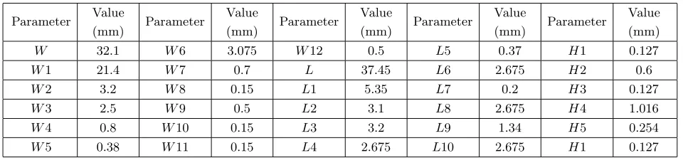
Table 5. Dimensions of the proposed antenna subarray.
Parameter Value (mm) Parameter Value (mm) Parameter Value (mm) Parameter Value (mm) Parameter Value (mm)
W 32.1 W6 3.075 W12 0.5 L5 0.37 H1 0.127
W1 21.4 W7 0.7 L 37.45 L6 2.675 H2 0.6
W2 3.2 W8 0.15 L1 5.35 L7 0.2 H3 0.127
W3 2.5 W9 0.5 L2 3.1 L8 2.675 H4 1.016
W4 0.8 W10 0.15 L3 3.2 L9 1.34 H5 0.254
Figure 9. Isolation analysis for the proposed feed network.
(a) (b)
Figure 10. Antenna subarray prototype, (a) substrate layers and (b) overall structure.
wideband coverage and gain maximization. The subarray dimensions are listed in Table 5.
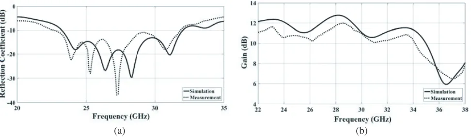
A subarray prototype, shown in Fig. 10, is then fabricated and tested. The main challenge of this design is to maintain good boresight gain across the FCC recommended bands. The simulated and measured reflection coefficients of the subarray are shown in Fig. 11(a). A measured impedance bandwidth of 33.4% (22.7–31.8 GHz) is achieved. We can notice an extra resonance is obtained compared with the unit cell element (i.e., four resonances at 24.2 GHz, 26.4 GHz, 28.3 GHz, and 31.1 GHz). This extra resonance is obtained due to the series resonance circuit of CF eed, LF eed and Lpost, as shown in
Fig. 7.
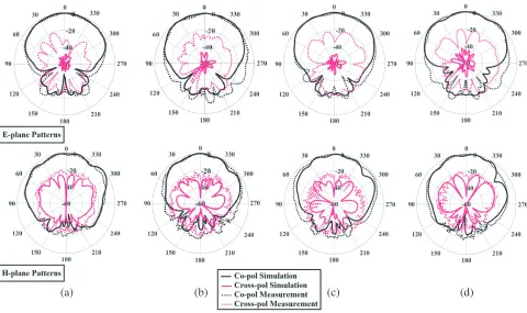
radiation patterns of the subarray at the center frequencies of the bands recommended by the FCC, i.e., 25.1 GHz, 27.9 GHZ, 29.2 GHz and 31.1 GHz. The measured HPBWs are 24◦, 23◦, 24◦, and 23◦ in the E-plane and 78◦, 77◦, 71◦ and 70◦ in the H-plane, respectively. The measured cross-polarized levels are less than−31.8 dB,−25.1 dB, −26.8 dB and−25.3 dB in theE-plane and less than −20.6 dB,
−20.7 dB,−20.4 and −23 dB in the H-plane, respectively. The simulation and measurement results of the subarray are summarized in Table 6.
The discrepancies between simulations and measurements are mainly due to fabrication tolerance and measurement alignment errors.
(a) (b)
Figure 11. Simulation and measurement results of the array, (a) reflection coefficient and (b) gain.
(a) (b) (c) (d)
Table 6. Simulation and measurement results of the subarray.
Parameter Simulations Measurements
Frequency Range (GHz) 23.2–32 22.7–31.8
Impedance Bandwidth 31.9% 33.4%
Gain Range (dB) 10.6–12.8 10–12
1-dB gain bandwidth 10.3% 10.5%
Frequency (GHz) 25.1 27.9 29.2 31.1 25.1 27.9 29.2 31.1 Gain (dB) 11.2 12.7 12.1 10.6 10.8 11.7 11.6 10.1 E-plane cross pol (dB) −40.8 −49.1 −46 −41.5 −31.8 −25.1 −26.8 −25.3 H-plane cross pol (dB) −30 −27.1 −28.3 −29.3 −20.6 −20.7 −20.4 −23 E-plane HPBW (degree) 23 26 25 23 24 23 24 23 H-plane HPBW (degree) 77 70 73 71 78 77 71 70 Front to back ratio (dB) −23.9 −27.6 −29.4 −27.2 −22 −22.2 −26.7 −22.6
4. CONCLUSION
This paper presents a novel design of a wideband 1x4 antenna subarray with high gain performance for the 5G applications at the mmW band. The subarray covers all frequency bands recommended for the next generation cellular network. The design uses proximity coupled stacked patches, which combine the advantages of the wideband coverage with less fabrication complexity in comparison with other fed techniques (i.e., coaxial fed), as well as maintaining the small spacing between the subarray elements. Klopfenstein tapering is applied along with two power dividers to design the feed network. The feed network achieves wideband operation, while maintaining good boresight gain, low cross polarization, and optimal space utilization. Prototypes of the proposed unit cell element and the antenna subarray have been fabricated and tested. The simulation and measurement results of the two prototypes are well matched. The subarray measurements demonstrate a wideband performance of 33.4% impedance bandwidth and 10.5% 1-dB gain bandwidth. The measured gain ranges between 10–12 dBi over the frequency band under consideration. The proposed subarray structure will then be used to design an adaptive beam antenna array for the 5G base station applications.
REFERENCES
1. Pi, Z. and F. Khan, “An introduction to millimeter-wave mobile broadband systems,” IEEE Commun. Mag., Vol. 49, No. 6, 101–107, Jun. 2011.
2. Rappaport, T. S., F. Gutierrez, E. Ben-Dor, J. N. Murdock, Y. Qiao, and J. I. Tamir, “Broadband millimeter-wave propagation measurements and models using adaptive-beam antennas for outdoor urban cellular communications,” IEEE Trans. Antennas Propag., Vol. 61, No. 4, 1850–1859, Apr. 2013.
3. Barati, C. N., S. A. Hosseini, S. Rangan, P. Liu, T. Korakis, S. S. Panwar, and T. S. Rappaport, “Directional cell discovery in millimeter-wave cellular networks,”IEEE Trans. Wireless Commun., Vol. 14, No. 12, 6664–6678, Dec. 2015.
4. Rajagopal, S., S. Abu-Surra, Z. Pi, and F. Khan, “Antenna array design for multi-Gbps mmWave mobile broadband communication,”IEEE Global Telecommunications Conf., Texas, USA, Dec. 5–9, 2011.
6. Rangan, S., T. S. Rappaport, and E. Erkip, “Millimeter-wave cellular wireless networks: Potentials and challenges,”Proc. IEEE, Vol. 102, No. 3, 366–385, Mar. 2014.
7. Ghosh, A., T. A. Thomas, M. C. Cudak, R. Ratasuk, P. Moorut, F. W. Vook, T. S. Rappaport, G. R. MacCartney, S. ‘Sun, and S. Nie, “Millimeter-wave enhanced local area systems: A high-data-rate approach for future wireless networks,” IEEE J. Sel. Areas Commun., Vol. 32, No. 6, 1152–1163, Jun. 2014.
8. Baldemair, R., T. Irnich, K. Balachandran, E. Dahlman, G. Mildh, Y. Sel´en, S. Parkvall, M. Meyer, and A. Osseiran, “Ultra-dense networks in millimeter-wave frequencies,” IEEE Commun. Mag., Vol. 53, No. 1, 202–208, Jan. 2015.
9. Pi, Z., J. Choi, and R. Heath, Jr., “Millimeter-wave gigabit broadband evolution toward 5G fixed access and backhaul,” IEEE Commun. Mag., Vol. 54, No. 4, 138–144, Apr. 2016.
10. Sulyman, A. I., A. T. Nassar, M. K. Samimi, G. R. Maccartney, T. S. Rappaport, and A. Alsanie, “Radio propagation path loss models for 5G cellular networks in the 28 GHz and 38 GHz millimeter-wave bands,”IEEE Commun. Mag., Vol. 52, No. 9, 78–86, Sep. 2014.
11. Samimi, M. K., T. S. Rappaport, and G. R. Maccartney, “Probabilistic omnidirectional path loss models form millimeter-wave outdoor communications,” IEEE Wireless Commun. Lett., Vol. 4, No. 4, 357–360, Aug. 2015.
12. Maccartney, G. R., T. S. Rappaport, M. Samimi, and S. Sun, “Millimeter-wave omnidirectional path loss data for small cell 5G channel modeling,” IEEE Access, Vol. 3., 1573–1580, Aug. 2015. 13. Maccartney, G. R., T. S. Rappaport, S. Sun, and S. Deng, “Indoor office wideband
millimeter-wave propagation measurements and channel models at 28 and 73 GHz for ultra-dense 5G wireless networks,” IEEE Trans. Wireless Commun., Vol. 3, 2388–2424, Oct. 2015.
14. Sun, S., T. S. Rappaport, T. A. Thomas, A. Ghosh, H. C. Nguyen, I. Z. Kovacs, I. Rodriguez, O. Koymen, and A. Partyka, “Investigatisn of prediction accuracy, sensitivity, and parameter stability of large-scale propagation path loss models for 5G wireless communications,”IEEE Trans. Veh. Technol., Vol. 65, No. 5, 2843–2860, May 2016.
15. Rappaport, T. S., G. R. Maccartney, M. K. Samimi, and S. Sun, “Wideband millimeter-wave propagation measurements and channel models for future wireless communication system design,” IEEE Trans. Commun., Vol. 63, No. 9, 3029–3056, Sep. 2015.
16. Wu, D., J. Wang, Y. Cai, and M. Guizani, “Millimeter-wave multimedia communications: Challenges, methodology, and applications,” IEEE Commun. Mag., Vol. 53, No. 1, 232–238, Jan. 2015.
17. Rajagopal, S., S. Abu-surra, J. C. Zhang, and F. Khan, “Power efficient signal processing for mm-Wave 5G systems,” J. Signal Process. Syst., Vol. 83, No. 2, 177–190, May 2016.
18. FCC, FCC 15-138, (2015, Oct. 23), [Online], Available: https://apps.fcc.gov/edocs public/attachmatch/FCC-15-138A1.pdf.
19. Aryanfar, F., J. Pi, H. Zhou, T. Henige, G. Xu, S. Abu-Surra, D. Psychoudakis, and F. Khan, “Millimeter-wave base station for mobile broadband communication,” IEEE MTT-S Int. Microw. Symp., Phoenix, USA, May 17–22, 2015.
20. Massa, A., M. Donelli, F. De Natale, S. Caorsi, and A. Lommi, “Planar antenna array control with genetic algorithms and adaptive array theory,” IEEE Trans. Antennas Propag., Vol. 52, No. 11, 2919–2924, Nov. 2004.
21. Azaro, R., G. Boato, M. Donelli, A. Massa, and E. Zeni, “Design of a prefractal monopolar antenna for 3.4–3.6 GHz Wi-Max band portable devices,”IEEE Ant. and Wireless Prop. Lett., Vol. 5, No. 4, 116–119, Apr. 2006.
22. Azaro, R., F. De Natale, M. Donelli, E. Zeni, and A. Massa, “Synthesis of a prefractal dual-band monopolar antenna for GPS applications,” IEEE Ant. and Wireless Prop. Lett., Vol. 5, No. 1, 361–364, Aug. 2006.
24. Donelli, M. and P. Febvre, “An inexpensive reconfigurable planar array for Wi-Fi applications,” Progress In Electromagnetics Research C, Vol. 28, 71–81, 2012.
25. Zhou, H. and F. Aryanfar, “A Ka-band patch antenna array with improved circular polarization,” IEEE Ant. and Prop. Soc. Int. Symp., Florida, USA, Jul. 7–13, 2013.
26. Zhou, H. and F. Aryanfar, “Millimeter-wave open ended SIW antenna with wide beam coverage,” IEEE Ant. and Prop. Soc. Int. Symp., Florida, USA, Jul. 7–13, 2013.
27. Phalak, K. and A. Sebak, “Aperture coupled microstrip patch antenna array for high gain at millimeter waves,” IEEE Int. Conf. Communication, Networks and Satellite, Jakarta, Indonesia, Nov. 4–5, 2014.
28. Elboushi, A. and A. Sebak, “High gain 4-element antenna array for millimeter-wave applications,” IEEE Int. Conf. Communication, Networks and Satellite, Jakarta, Indonesia, Nov. 4–5, 2014. 29. Ashraf, N., O. M. Haraz, M. M. M. Ali, M. A. Ashraf, and S. A. S. Alshebili, “Optimized broadband
and dual-band printed slot antennas for future millimeter-wave mobile communication,” Int. J. Electron. Commun., Vol. 70, No. 3, 257–264, Mar. 2016.
30. Psychoudakis, D., Z. Wang, and F. Aryanfar, “Dipole array for mm-wave mobile applications,” IEEE Antenna and Propagation Soc. Int. Symp., Florida, USA, Jul. 7–13, 2013.
31. Haraz, O. M., A. Elboushi, S. A. Alshebeili, and A. R. Sebak, “Dense dielectric patch array antenna with improved radiation characteristics using EBG ground structure and dielectric superstrate for future 5G cellular networks,” IEEE Access, Vol. 2, 909–913, Aug. 2014.
32. Zhai, W., V. Miraftab, and M. Repeta, “Broadband antenna array with low cost PCB-substrate for 5G millimeter-wave applications,” Global Symp. Millimeter Waves, Quebec, Canada, May 25–27, 2015.
33. Pozar, D. M. and B. Kaufman, “Increasing the bandwidth of a microstrip antenna by proximity coupling,”Electron. Lett., Vol. 23, No. 8, 368–369, Apr. 1987.
34. Pozar, D. M., “Microstrip antennas,” Proc. IEEE, Vol. 80, No. 1, 79–91, Jan. 1992.
35. Rowe, W. S. T. and R. B. Waterhouse, “Investigation into the performance of proximity coupled stacked patches,”IEEE Trans. Antennas Propag., Vol. 54, No. 6, 1693–1698, Jun. 2006.
36. Lee, R. Q., K. F. Lee, and J. Bobinchak, “Characteristics of a two-layer electromagnetically coupled rectangular patch antenna,”Electronics Lett., Vol. 23, No. 20, 1070–1072, Sep. 1987.
37. Balanis, C. A.,Antenna Theory: Analysis and Design, 3rd edition, New Jersey, Wiley, 2005. 38. Li, Y., W. Li, Q. Ye, and R. Mittra, “A survey of planar ultra-wideband antenna designs and
their applications,” Forum for Electromagnetic Research Methods and Application Technologies, Aug. 2014.
39. Garg, R., P. Bhartia, I. Bahl, and A. Ittipiboon,Microstrip Antenna Design Handbook, 1st edition, Boston• London, Artech House, 2001.
40. Meshram, M. K., “Analysis of L-strip proximity fed rectangular microstrip antenna for mobile base station,”Microw. Opt. Techn. Lett., Vol. 49, No. 8, 1817–1824, Aug. 2007.
41. Hong, J. G. and M. J. Lancaster, Microstrip Filters for RF/Microwave Applications, New York, Wiley, 2001.
42. Ershadi, S. E., A. Keshtkar, A. H. Abdelrahman, X. Yu, and H. Xin, “Design of wideband unit-cell element for 5G antenna arrays,”Asia-Pacific Microwave Conf., Nanjing, China, Dec. 6–9, 2015. 43. Hansen, R. C., Phased Array Antennas, 2nd edition, New Jersey, Wiley, 2009.
44. Pozar, D. M., Microwave Engineering, 4th edition, New York, Wiley, 2012