Available online: https://pen2print.org/index.php/ijr/ P a g e | 596
Light-Load Efficiency Power Conversion Scheme Using Bidirectional Buck
Converter
SANDYAVARI SWAPNA PRIYA K.NARASIMHAIAHACHARIM.Tech,(Ph.D)
M.Tech Student Dept of EEE Associate Professor ,Dept of EEE,
G.Pullaiah college of Engineering and Technology G.Pullaiah college of Engineering and Technology
Kurnool (Dist) ,A.P Kurnool (Dist) ,A.P
Abstract: High efficiency under a light-load condition is becoming important ,because power systems operate mostly under this condition. In the current social atmosphere promoting energy savings, high
efficiency is valued for server power supplies in data centers to reduce power consumption. For this
reason, many programs and regulations require high light-load efficiency. In this project, a new power
conversion scheme considering paralleled modules is to be proposed. Under a very light-load condition,
only a non-isolated buck converter in the secondary side of the remaining power supply provides the
output power, which is different from the cold-redundant (CR) concept.Furthermore,in the proposed
concept, the voltage source in the buck converter is maximized by using an additional voltage bus
connecting between the snubber capacitors of each module. To achieve high power density, the buck
converter is integrated with the rectifier circuits in the secondary side of the Phase shift full-bridge(PSFB)
converter. The validity of the basic operational principles is confirmed with two 12V/750W by using
MATLAB/ simulink software .The results will be demonstrated for the proposed converter.
Key words—Bidirectional, buck converter, integrated, light-load efficiency, paralleled, power conversion,
server power supply.
I.INTODUCTION
IN the current social atmosphere promoting energy savings, high efficiency is valued for server power supplies in data centers to reduce power consumption. Especially, high efficiency under a light-load condition is becoming important, because power systems operate mostly under that condition. For this reason, many programs and regulations require high light-load efficiency. For example, the 80 PLUS performance specification requires power
supplies in computers and servers to be high efficient To achieve Titanium certification, the efficiency must be satisfied mostly to be greater than 90% at 10 % load, as well as under a
full-load condition. Furthermore, many
Available online: https://pen2print.org/index.php/ijr/ P a g e | 597 and network equipment require high light-load
. efficiency even below a 5% load condition, which exceeds the latest Energy Star specifications .This means that very light-load efficiency will become more important in the future.
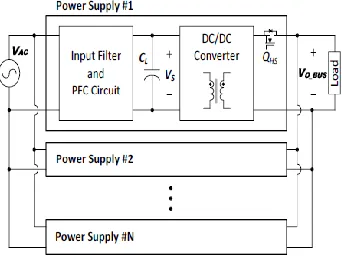
Fig. 1 shows the general structure of a server power supply. The N power supplies are connected in parallel and provide the output power with an equally shared load current. This increases the power handling capability and the overall efficiency. Additionally, redundant power supplies are normally adopted in this structure. These enable the power to be supplied continuously even when an arbitrary power supply is turned off due to faults, which improves overall reliability . Each power supply has two power conversion stages. The first one is the input filter and the power-factor-correction (PFC) circuit, which creates low EMI, surge protection, and a high power factor. The PFC circuit, normally using a boost converter, converts the AC voltage to DC link voltage VS
of about 400V. The second power conversion stage is the DC/DC power conversion circuits, which use an isolation transformer and regulate
the output voltage at about 12V. A phase-shift full-bridge (PSFB) converter is generally used to meet the high step-down voltage, low output voltage and high output current. In DC/DC power conversion, many components, including many switches and magnetic components, are used, so it is very difficult to improve the overall efficiency, especially under a light-load condition, due to the switching and core losses. Meanwhile, hot-swap circuits using a switch
QHS and load-share control circuits are additionally required to connect and drive the paralleled power supplies.
Available online: https://pen2print.org/index.php/ijr/ P a g e | 598 conduction loss which means lower heavy-load
efficiency. In [9], the power converter operates according to the load power with maximum efficiency by changing the dc-link voltage and the switching method. According to the load condition, the switching mode of the PSFB converter is changed into the PWM and burst modes. Thus, the light-load efficiency is increased by minimizing the switching and circulating conduction losses. Another approach is to consider paralleled modules, not limited to a single module. The cold-redundant (CR) concept is proposed in [10]-[13]. Under a certain light-load condition, the DC/DC converter in the redundant power supply is turned off and enters standby mode, so the remaining modules provide the total output power, which eliminates the switching, core, and control losses in the DC/DC converter of the redundant power supply.
In this paper, a new power conversion scheme considering paralleled modules is proposed. Under a light-load condition, the redundant power supply enters standby mode as in the CR concept. However, under a very light-load condition, only a non-isolated buck converter in the secondary side of the remaining power supply provides the output power, which is different from the CR concept. Thus, the operating components and the related power losses are more minimized. Also, to achieve high power density, the buck converter is integrated with the rectifier circuits in the secondary side of the PSFB converter. Furthermore, in the proposed concept, the voltage source in the buck converter is maximized by using an additional voltage bus
connecting between the snubber capacitors of each module.
II. PROPOSED CIRCUIT AND
OPERATION
Fig. 2 shows the circuit diagram of a PSFB converter. PSFB converters are widely used in low-voltage, high-current and high-power applications due to its low output current stress achieved by using an output inductor (LO), which results in low overall conduction loss. Also, because the full-bridge inverter is controlled via phase-shifts, ZVS can easily be achieved by using transformer leakage inductance (Llkg). Another feature is the RCD snubber. To reduce the voltage stresses on the SRs and to be able to use low-voltage-rated switches, the snubber capacitor (CA) in the RCD snubber, indicated in red box in Fig. 2, clamps the voltages of the SRs and its energy is dissipated to the output voltage (VO) through
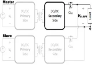
Available online: https://pen2print.org/index.php/ijr/ P a g e | 599 Fig. 3 shows the CR concept in two power
supplies. For example, above a 20% load condition, the two power supplies have equal load currents, which is called the load share mode. On the other hand, below a 20% load condition, one power supply is turned off, and another power supply has the entire load current which provides high light-load efficiency. The turned-off power supply is called the slave, and the other is called the master. However, the overall efficiency is still low under a very light-load condition. For example, the efficiency at 1% load condition is about 50% in 12V / 750W output. Therefore, in this paper, to improve the overall efficiency under very light-load efficiency, a new power conversion scheme is proposed. In order to explain the proposed circuit and operation easily, this chapter is divided into three parts: 1) concept of proposed circuit, 2) implementation of proposed circuit, 3) operational principles of proposed circuit.
A.Concept of proposed circuit
This part explains the concept of the proposed circuit. Under a light-load condition, the proposed circuit operates like the conventional CR concept, as shown in Fig. 3. On the other hand, under a very light-load condition, the primary-side circuits in the master are turned off, as shown in Fig. 4. Thus, only the secondary-side circuits in the master transfers power to the load,
III.IMPLEMENTATION OF PROPOSED CIRCUIT
In this part, the implementation of the proposed circuit is explained to realize the concept of the proposed circuit. Fig. 7 shows the proposed circuit employing the PSFB converter where
Available online: https://pen2print.org/index.php/ijr/ P a g e | 600 the energy of VAUX can be maximized in
the
pa ralleled modules. Therefore, VAUX can be used as a new voltage source under a very light-load condition.
Secondly, the bidirectional converter is required to not only transfer power to the load but also charge VAUX effectively. Meanwhile, the bidirectional buck converter is widely used for non-isolation and bidirectional power flow due to its simple structure and high efficiency [15]-[18]. Thus, the bidirectional buck converter is applied to the proposed circuit for transferring power from VAUX-BUS to the load and charging
VAUX-BUS from the slave. Fortunately, with small changes, the bidirectional buck converter can be easily integrated into the secondary-side circuit of the PSFB converter. By using the switches (QA1 and QA2) instead of the diodes of the RCD snubber (DA1 and DA2), two bidirectional buck converters with one inductor
LO are integrated. The output inductor current
iLOis equally divided into two bidirectional buck converters with the help of the transformer secondary windings (NS) which are coupled to each other with same turns. Therefore, the proposed concept can be implemented very
effectively in converters which have a center-tap rectifier with SRs and an output inductor.
IV.OPERATIONAL PRINCIPLES OF PROPOSED CIRCUIT
In this part, the operational principles of the proposed circuit are explained by dividing operation mode into the charging mode and discharging mode. Fig. 8 shows the operating modes of the proposed circuit under a very light-load condition and Fig. 9 shows the key waveforms of the bidirectional buck converter. In these figures, the reference direction of iLOis expressed as the charging direction of CA. In addition, to simplify the analysis, it is assumed that the dead times between the gate signals are neglected.
1) Discharging mode
In the discharging mode, the slave is turned off, and only the bidirectional buck converter operates and transfers power from VAUX-BUS
to the load by using the energy stored in CA, as shown in Fig. 8(a). Firstly, when QA1 and QA2
Available online: https://pen2print.org/index.php/ijr/ P a g e | 601
iLObuilds up with a slope of (VO_BUS
-VAUX)/LO. After QA1 and QA2 are turned off and Q5 and Q6 are turned on, iLOdecreases to zero with a slope of VO_BUS/LO as shown in Fig. 9(a).
2) Charging mode
In the charging mode, the primary-side of the master is still turned off but the slave is turned on. Thus, the slave transferspower to the load and charges CA by using the bidirectional buck converter with the boost
V.DESIGN CONSIDERATIONS
To use the proposed circuit effectively, the design consideration of the bidirectional buck converter is required. Therefore, in this chapter, VAUX, CA, DBuck, and DBoostof the bidirectional buck converter are explained except for LO because LO is already designed by the PSFB converter.
VAUX
To obtain sufficient energy from CA under a very light-load condition, the voltage swing range of VAUX should be maximized. However, since VAUX is also used as the snubber voltage over a light-load condition, the range of VAUX should not affect the operation of the PSFB. Thus, in designing VAUX, the snubber voltage range of the PSFB operation should be considered. Firstly, VAUX_MIN is determined by the minimum snubber voltage, which is expressed as follows:
whereVS_MAX is the maximum link voltage, and NP and NS are the transformer primary and
secondary turns, respectively. Thus, VAUX_MIN can be designed as 30V according to the design parameters of the PSFB converter, where VS_MAX=400V, NP=27, and NS=1. Secondly, VAUX_MAX is determined by considering the voltage stresses on SRs. In general, the PSFB converter
providing 12V output uses 60V voltage-rated switches for SRs because SRs of the PSFB converter suffer from the additional voltage spike caused by the resonance between the leakage inductor of the transformer and junction capacitor of SRs, Therefore, with the 50% voltage margin, VAUX_MAX is designed as 40V to use 60V voltage-rated switches. As a result, the range of VAUX is designed as 30-40V.
CA
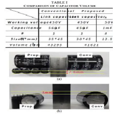
Available online: https://pen2print.org/index.php/ijr/ P a g e | 602 density. Moreover, since the size of aluminum
electrolytic capacitor can be more increased as the capacitance is increased, CA should be designed by considering the power density. Meanwhile, the sever power supply has a special requirement called the hold-up time (TH), where VO_BUS stays within a regulated range by using the energy stored in the DC link capacitor (CL) after AC is lost. That means CL is inevitably large to provide power for the load without AC source. However, since VAUX can be used another voltage source during the hold-up time, CA can help the hold-hold-up time to be extended. Conversely, CL can be designed to be smaller while maintaining the same TH. The relation between CL and CA is written as follows:
In practical circuits, the switching stress is much higher because of the parasitic inductance (Lp) and capacitance (Cp). Cp includes the output capacitance of the switch and stray capacitance due to PCB layout and mounting. Lp includes the parasitic inductance of the PCB route and MOSFET lead inductance. These parasitic inductances and capacitances from the power devices form a filter that resonates right after the turn-off transient, and therefore superimposes excessive voltage ringing to the devices as shown in Figure 3. To suppress the peak voltage, a typical RC snubber is applied across the switch as shown in Figure 4. The value of the resistor must be close to the impedance of the parasitic resonance which it is intended to damp. The snubber capacitance must be larger than the resonant circuit capacitance, but must be small enough in order to keep the power dissipation of the resistor to a minimum.
whereVS_MIN is the minimum link voltage, PO_REQ is the required output power for the hold-up time, η is the efficiency of the DC/DC converter, and CL_C and CL_P are the link capacitance in the conventional and proposed
converters, respectively. When
VS_MAX=400V, VS_MIN=340V, and CL_C =560μF, from (2), CL_P and CA can be designed as 470μF and 1mF*4 by considering the size of CL_C and CL_P+CA. Table I shows the capacitor volume and Fig. 10 shows the overall capacitors size in the proposed and conventional converters. In summary, although the proposed circuit has a large CA, it has a smaller total capacitor volume because CA can help the size of DC link capacitor to be reduced. DBuck and DBoost
The buck duty ratio (DBuck) is naturally determined by IO to regulate VO_BUS, which is expressed as follows:
Available online: https://pen2print.org/index.php/ijr/ P a g e | 603 Meanwhile, since the boost duty ratio (DBoost)
decides the charging current (ICH), it relates to the charging time, which affects the overall all efficiency. The expected efficiency in the proposed circuit can be expressed as follows:
wherePO is the output power, PLoss_CHis the power loss in the charging mode, TCH and TDISCH are the charging and discharging times, respectively, and TPeriodis the sum of TCH and TDISCH, as shown in Fig. 6. TDISCH is determined by the PO and power loss during the discharging time. From (4), to achieve high efficiency under a very light-load condition, TCH should be minimized because PLoss_CHis additionally caused during TCH.
However, the shorter TCH requires larger ICH and Dboost, which creates higher current stress on CA as well as conduction loss.
Thus, the maximum current stress of CA should be considered to decide DBoost.
VISIMULATION RESULTS
A.SIMULINK DIAGRAM OF PROPOSED CIRCUIT
Fig 8(a) SIMULINK DIAGRAM OF PROPOSED CIRCUIT
Fig 8(b) Out put
B.SIMULINK DIAGRAM OF
Available online: https://pen2print.org/index.php/ijr/ P a g e | 604 Fig 9(a)SIMULINK DIAGRAM OF DISCHARGING MODE
Fig 9(b) Out Put
In the discharging mode, the slave is turned off,
and only the bidirectional buck converter
operates and transfers power from VAUX-BUS
to the load by using the energy stored in CA, as
shown in Fig. 8(a). Firstly, when QA1 and QA2
are turned on and Q5 and Q6 are turned off,
iLObuilds up with a slope of
(VO_BUS-VAUX)/LO. After QA1 and QA2 are turned off
and Q5 and Q6 are turned on, iLOdecreases to
zero with a slope of VO_BUS/LO as shown in
above Figure.
C.SIMULINK DIAGRAM OF CHARGING MODE
Available online: https://pen2print.org/index.php/ijr/ P a g e | 605 Fig10(b) Out Put
In the charging mode, the primary-side of the
master is still turned off but the slave is turned
on. Thus, the slave transfers power to the load
and charges CA by using the bidirectional buck
converter with the boost operation, as shown in
above Figure.
Snubbers are frequently used in electrical
systems with an inductive load where the sudden
interruption of current flow leads to a sharp rise
in voltage across the current switching device
("inductive kick"), in accordance with Faraday's
law. This transient can be a source
of electromagnetic interference (EMI) in other
circuits. Additionally, if the voltage generated
across the device is beyond what the device is
intended to tolerate, it may damage or destroy it.
The snubber provides a short-term alternative
current path around the current switching device
so that the inductive element may be discharged
moresafely and quietly. Inductive elements are
often unintentional, but arise from the current
loops implied by physical circuitry. While
current switching is everywhere, snubbers will
generally only be required where a major current
path is switched, such as in power supplies.
Snubbers are also often used to
prevent arcing across the contacts of relays and
switches and the electricalinterference
and welding or sticking of the contacts that can
occur (see also arc suppression).
VII.CONCLUSION
A new power conversion scheme is presented using paralleled modules is to be proposed. Under a very light-load condition, converter achieved high efficiency by using an integrated bidirectional buck converter. The buck converter is integrated easily by using switches instead of snubber diodes. By connecting the snubber voltage from each module and by using it as additional voltage bus, an auxiliary voltage source is effectively obtained for the buck converter. In this project the circuit operation and design considerations are illustrated. The validity of the basic operational principles is confirmed with two 12V/750W by using MATLAB/Simulink software. The results will be demonstrated for the proposed converter. REFERENCES
[1] 80 Plus Incentive Program. [Online]. Available: http://www.80plus.org
Available online: https://pen2print.org/index.php/ijr/ P a g e | 606 Specifications [Online]. Available:
http://www.energystar.gov/index.cfm?c=archive s.computer_spec_version_5_0
[3] S. Luo and I. Batarseh, “A review of distributed power systems Part I: DC distributed power system,” IEEE Aerosp. Electron. Syst. Mag., vol. 20, no. 8, pp. 5–16, Aug. 2005.
[4] H.-S Kim, J.-K. Kim, K.-B. Park, H.-W. Seong, G.-W. Moon, and M.-K. Youn, “On/Off Control of Boost PFC Converters to Improve Light-Load Efficiency in Paralleled Power Supply Units for Server,” in IEEE Trans. Ind. Electron., vol. 61, no. 3, pp. 1235–1242, Mar. 2014.
[5] J.-W. Kim, D.-Y. Kim, C.-E. Kim, and G.-W. Moon, “A simple switching control technique for improving light load efficiency in a phase-shifted full-bridge converter with a server power system,” in IEEE Trans. Power Electron., vol. 29, no. 4, pp. 1562-1566, Apr. 2014.
[6] J.-H. Kim, J.-K. Kim, J.-B. Lee, and G.-W. Moon, “Load Adaptive Gate Driving Method for High Efficiency Under Light-Load Conditions,” in IEEE Trans. Ind. Electron., vol. 61, no. 9, pp. 4674-4679, Sep. 2014.
[7] Y.-S. Lai and Z.-J. Su, “Novel on-line maximum duty point tracking technique to improve two-stage server power efficiency and investigation into its impact on hold-up time,” in
IEEE Trans. Ind. Electron., vol. 61, no. 5, pp. 2252-2263, May. 2014.
[8] M. Narimani and G. Moschopoulos, “An investigation on the novel use of high-power three-level converter topologies to improve light-load efficiency in low power DC/DC full-bridge converters,” in IEEE Trans. Ind.
Electron., vol. 61, no. 10, pp. 5690-5692, Oct. 2014.
[9] Y.-S. Lai and Z.-J. Su, “New Integrated Control Technique for Two-Stage Server Power to Improve Efficiency Under the Light-Load Condition,” in IEEE Trans. Ind. Electron., vol. 62, no. 11, pp. 6944-6954, Nov. 2015.
[10] Intel Corporation, Intel server system SR2625UR technical product specification 2012. [Online]. Available: http://download.intel.com/ support/motherboards/server/s5520ur/sb/e46130 010_sr2625ur_tps_r1_9.pdf
[11] S. Belson and S. L. Harris, “Power system with plural parallel power supplies with at least one power supply in standby mode for energy efficiency,” U.S. Patent 6 614 133, Sep. 2, 2003. [12] S. A. Berke and M. Muccini, “System and method for power supply warm spare and programmable load sharing,” U.S. Patent 8 645 739, Feb. 4, 2014.
[13] V. Vogman, “Reducing power losses in a redundant power supply system,” U.S. Patent 2014/0035375, Feb. 6, 2014.
[14] S.-Y. Lin and C.-L. Chen, “Analysis and design for RCD clamped snubber used in output rectifier of phase-shift full-bridge ZVS converters,” in IEEE Trans. Ind. Electron., vol. 45, no. 2, pp. 358-359, Apr. 1998.
[15] M. Orabi and A. Shawky, “Proposed switching losses model for integrated point-of-load synchronous buck converter,” in IEEE Trans. Power Electron., vol. 30, no. 9, pp. 5136-5150, Sep. 2015.
Available online: https://pen2print.org/index.php/ijr/ P a g e | 607
Trans. Ind. Electron., vol. 62 no. 2 pp. 991-1001, Feb. 2015.
[17] M. R. Mohammadi and H. Farzanehfard, “A New Family of Zero-Voltage-Transition Nonisolated Bidirectional Converters With Simple Auxiliary Circuit,” in IEEE Trans. Ind. Electron., vol. 63, no. 3, pp. 1519-1527, Mar. 2016.