D. Ramya
M.Tech (VLSI) Dept of E.C.E
Chaitanya Institute of Technology and Science, Warangal, Telangana,India
Email: [email protected]
Dr. B. SHOBA RANI
Associate Professor Dept of E.C.E
Chaitanya Institute of Technology and Science, Warangal, Telangana,India
Email: [email protected]
ABSTRACT: In order to enhance the leakage performance in conventional CMOS systems, we use advanced computing systems. This computing system contains embed spintronic devices. The both magnetic tunnel junction (MTI) and a spintronic device has high speed, low power and infinite endurance properties. These are most widely used in logic circuits. In this present paper we use a penta MTJ based logic gate, this logic gate has easy cascading, self referencing properties. The penta MTJ based logic gates are existed in pre charge sense amplifier and low area overhead countary which provides disturbance free reading and increased tolerance. Because of this in CMOS process there is a compatibility to process variations. Basically, the logic gates ate simulated at 45nm technology by using a verilog A model of penta MTJ.
I. INTRODUCTION
As we know that all the digital signals are denoted in conventional CMOS logic with or without presence of electric charge in terms of voltage vdd or ground. Actually, spintronic is nothing but to store the information and charge the process. In spintronic there is possibility to change CMOS logic and memory. The digital signals in spintronic are given by up and down spin of electrons. The most widely used device of spintronic is magnetic tunnel junction (MTJ). This operates on the principle of tunnel magneto resistance (TMR) and consists of ferromagnetic layers which are divided by a oxide layer. This enhance the performance of
CMOS logic circuit and fabricated by using 3-D backend integration process. Processing and storage properties in penta MTJ helps to minimize the memory and inter connect delay power. This stores the processed back onto memory but here some drawbacks are occurred in magnetic logic gate. Basically, a magnetic XOR gate consists of 6 MTJ's and transistors. If number of MTJ's increases, there will be serious limitations in hybrid circuit that contains both CMOS and MTJ. To commute the voltage signal to current signal there should be effective magnitude. By selecting initial state and operating voltage we can realize the logic operations in MTJ. There are two logic gates, one is linear and another one is non linear. Linear logic uses NAND, NOR functions and non linear logic uses two input
XOR/XNOR that are implemented on
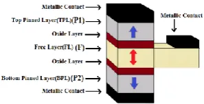
NAND/NOR gates. Here non linear logic gates involve operation in 3 stages they are , 1) Fundamental 2) Horowitz and Hill existed spin diode logic family & 3)CMOS logic gate. A penta MTJ contains 2 pinned ferromagnetic layers and one free layer. In the middle of pinned and free layer we use Mgo which is shown in fig (1). In this parallel and anti parallel states are 2 resistance states that are used in conventional MTJ. By using this penta MTJ realization in digital circuits, there are many advantages like 1) It does not require any reference circuit due to presence of 2 pinned layer. 2) In complementary outputs there is no need of extra hardware due to presence of pre charge sense amplifier. 3)
Fast Pipelined Storage for High-Performancecascaded Penta Mtj-Based
There is no need to initialize the state of output MTJ because it is directly sensed by PCSA.
Because of this the sensing power
consumption is reduced and speed is enhanced. At last by connecting in series it gives perfect contribution to our proposed magnetic logic gates. This occurs due to output of logic gate and programming signal of penta MTJ are voltage signals .
II. STATE OF ART
A. Penta MTJ
From figure (1) we can observe the structure of penta MTJ. It consists of two pinned layers, one Is top pinned layer (TPL) another one is bottom pinned layer (BPL). Both these layers are fixed in opposite direction. There are two states in penta MTJ 1state and 0 state. 1 state is assumed when TPL is parallel to free layer and 0 state is assumed when BPL is parallel to free layer. As compared to conventional MTJ, the proposed structure penta MTJ requires
less power. In this current is used to convert parallel to anti parallel state for one stack .As discussed earlier that penta MTJ obtains disturbance free reading and increases the tolerance to process the variation. In micro magnetic simulation, the dual pinned layer with single free layer structure of penta MTJ Is existed. We know that penta MTJ has lower resistance than the conventional MTJ.
Fig. 1. Structure of PentaMTJ with two pinned layers (TPL and BPL) and one free layer.
B. Logic in memory
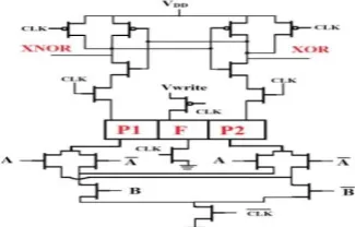
Fig 2 shows the block diagram for logic in memory. It mainly includes into three parts.1.PCSA for sensing the difference
between two 2.penta MTJ logic .3.PCSA is used to sense the difference between two states of resistance and it is dynamic logic ckt.4.it has two phases one is pre phase and another is evaluation phase. In the discharging of branches occurred depends on the o/p mode of returns resistances. Relative resistance ate lower resistance that discharge the output node capacitance to cut off the other branch. Basically, low resistance branch pulls down towards the ground and high resistance branch pulls up towards the vdd. Now in proposed structures there are low reading disturbance and dynamic sensing capabilities which reduce the delay power. Both writing path and pre charging in penta MTJ are separated by nMOS transistors MN2 and MN3. There are two limitations of PCSA that unbound the proposed logic gates.
One is due to mismatch occurred in
MTJ/CMOS, another one is due single stacking causes low PVT variation. The writing path of penta MTJ moves only in one direction (I.e.) from anti parallel state to
parallel state. This phase starts with
connection of free layer to vdd by determining the stack of parallel writing. Here nMOS MN6 obtains efficient writing in penta MTJ.
Fig. 2. (a) Block diagram of logic gates using PentaMTJ. (b) Writing, state detection, and amplification using PCSA of
PentaMTJ cell.
III. LOGIC GATE USING PENTA MTJ
sensing position is same for every logic gate. Depending upon the serial or parallel combinations of transistors of transistors the information is stored. In penta MTJ storing of information involves two formats one is storing 0 and storing 1. In storing 1 process all the logic combinations which has high output are combined and the result is expressed by using k-map. In storing 0 process the complementary of expansion is evaluated. The simulation result of logic gates of both normal
and complementary outputs ate shown in fig
(4). Here A & B ate 2 inputs,0 indicates discharging of PCSA and 1 indicates that there is no charging of normal output.
Fig.3. XOR/XNOR gates using PentaMTJ
Fig. 4. Simulation result of XOR/XNOR gate1154
IV. 3-BIT GRAY COUNTER
As we know that sequential logic circuits are obtained from combinational logic circuit. In this the output of sequential logic circuit depends on previous output and present input. In 3-bit gray counter we use a sequential logic circuit, these are obtained on as one digit. Now
let us discuss the present state which are formed in gray counter. In this the values are stored in flip flops and power is consumed understand by condition. By using penta MTJ in sequential circuits it stores counter values in previous state rather than in initial state. In gray counter we use PCSA to sense the circuit and it produces output in next state.
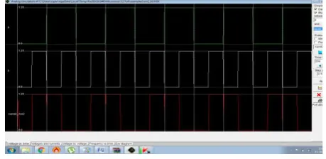
Below figure (5) shows the circuit diagram of 3-bit gray counter by using penta MTJ. In this there are 3 penta MTJ's for the purpose of storage, 3 PCSA's for the purpose of sensing and it consists of writing unit which consists of inter connection of transistors. Here An, Bn, Cn are the outputs that are stored in present state and An+1, Bn+1 and Cn+1 are the values of next state that are stored in penta MTJ. The operation begins with writing in penta MTJ by using clock with pulse width 1.5ns. To attain the writing in penta MTJ with 1.5ns then a clock width of 2ns time period and 1.5ns time periods are generated. When clock width is high than Pre charging and sensing operations are performed by using a short duration high CLKR pulse (200 ps). Until the counter stops the process will be repeated. From figure (6) we can see the simulation result of most significant bit (I.e) Cn+1 and least significant bit (I.e.) An+1.
Fig. 6. Simulation result of Proposed system
V. CONCLUSION
By using penta MTJ in digital circuits it gives low static power, short inter connect delay and effective power gating . This penta MTJ logic minimizes the area by removing intermediate circuitry and provide conversion of current to voltage and voltage to current. While performing logic operations there will be no initial conditions and it eliminates the extra MTJ's by us on reference properties. At lat we can say that by using penta MTJ it gives perfect disturbance free reading and increased tolerance to process the variations.
VI.REFERENCES
[1] S. Tehrani et al., “Recent developments in
magnetic tunnel junction MRAM,” IEEE
Trans. Magn., vol. 36, no. 5, pp. 2752–2757, Sep. 2000.
[2] G. A. Prinz, “Magnetoelectronics,” Science, vol. 282, pp. 1660–1663, Nov. 1998.
[3] ERD. (2011). International Roadmap for
Semiconductor (ITRS). [Online]. Available: http://www.itrs.net/Links/2011ITRS/Home201 1.htm
[4] S. Parkin, X. Jiang, C. Kaiser, A. Panchula, K. Roche, and M. Samant, “Magnetically engineered spintronic sensors and memory,” Proc. IEEE, vol. 91, no. 5, pp. 661–680, May 2003.
[5] S. A. Wolf et al., “Spintronics: A
spin-based electronics vision for the future,” Science, vol. 294, no. 5546, pp. 1488–1495, 2001.
[6] C. Chappert, A. Fert, and F. N. Van Dau, “The emergence of spin electronics in data
storage,” Nature Mater., vol. 6, no. 11, pp.
813–823, Nov. 2007.
[7] S. D. Pable and M. Hasan, “Interconnect
design for subthreshold circuits,” IEEE Trans.
Nanotechnol., vol. 11, no. 3, pp. 633–639, May 2012.
[8] H.-P. Trinh, W. Zhao, J.-O. Klein, Y. Zhang, D. Ravelsona, and C. Chappert, “Magnetic adder based on racetrack memory,” IEEE Trans. Circuits Syst. I, Reg. Papers, vol. 60, no. 6, pp. 1469–1477, Jun. 2013.
[9] S. Lee, N. Kim, H. Yang, G. Lee, S. Lee, and H. Shin, “The 3-bit gray counter based on
magnetic-tunnel-junction elements,” IEEE
Trans.Magn., vol. 43, no. 6, pp. 2677–2679, Jun. 2007.
[10] A. Lyle et al., “Magnetic tunnel junction
logic architecture for realization of
simultaneous computation and
communication,” IEEE Trans. Magn., vol. 47,
no. 10, pp. 2970–2973, Oct. 2011.
[11] J. S. Friedman, N. Rangaraju, Y. I. Ismail, and B. W. Wessels, “A spin-diode logic
family,” IEEE Trans. Nanotechnol., vol. 11,
no. 5, pp. 1026–1032, Sep. 2012.
[12] P. Horowitz and W. Hill, The Art of
Electronics. Cambridge, U.K.: Cambridge Univ. Press, 1989.
[13] S. Huda and A. Sheikholeslami, “A novel STT-MRAM cell with disturbance-free read
operation,” IEEE Trans. Circuits Syst. I, Reg.
Papers, vol. 60, no. 6, pp. 1534–1547, Jun. 2013.
[14] M. K. Gupta and M. Hasan, “Design of high speed energy efficient masking error
immune PentaMTJ based TCAM,” IEEE
Trans. Magn., no. 99.
[15] W. Xu, T. Zhang, and Y. Chen, “Design of spin-torque transfer magnetoresistive RAM and CAM/TCAM with high sensing and
search speed,” IEEE Trans. Very Large Scale
Integr. (VLSI) Syst., vol. 18, no. 1, pp. 66–74, Jan. 2010.
Authors:
Dr. B. SHOBA RANI working as Associate