ISSN(Online): 2319-8753 ISSN (Print): 2347-6710
I
nternational
J
ournal of
I
nnovative
R
esearch in
S
cience,
E
ngineering and
T
echnology
(A High Impact Factor, Monthly, Peer Reviewed Journal) Visit: www.ijirset.com
Vol. 8, Issue 8, August 2019
Design Low Power of SRAM Cells in Ultra
Deep Submicron CMOS Technology
Sitaram Chowdhary, Dr. Surendra Bohra
Research Scholar M. Tech. (VLSI), SLBS Engineering College, Jodhpur, India Professor & Principal, SLBS Engineering College, Jodhpur, India
ABSTRACT: Static Random Access Memories (SRAMs) are used in a wide variety of applications ranging from ICs to embedded systems and high performance processors to mobile phone chips. In these applications high integration density, low power and fast performance are all critical parameters. To achieve these objectives, the feature size of CMOS devices has been dramatically scaled to very small dimensions.
This dissertation explores the design and analysis of Static Random Access Memories (SRAMs), focusing on optimizing delay and dynamic power. Memory access incorporates two different operations: the memory read and the memory write. Owing to high bitline voltage swing during write operation, the write power consumption is dominated the dynamic power consumption. To improve the performance of the memory write operation different cell designs are suggested by variations in basic 6T SRAM cell. Since short-circuits are responsible for much of the dynamic power loss, concept of virtual source transistors is used for removing direct connection between VDD and GND. Faster write time can be achieved by using
transmission gates instead of simple NMOS pass transistors.
I. INTRODUCTION
The goal of this research is to develop variations of the standard 6T SRAM cell to analyze dynamic power and delay in write mode. By using different combinations of virtual source transistors along with the CMOS transmission gates, seven distinct designs for SRAM cells are created to accomplish this goal.
The objectives of this research include:
Develop a novel family of SRAM cells designed for removal of wasteful sources of dynamic power consumption that result from short circuits that exist when the memory cell is switching.
Determine the performance of each cell structure.
Evaluate merits and demerits by comparing power and delay performance of these structures.
Estimate the area of each memory cell by minimum device dimensions of process technology.
II. BASICS OF SRAM CELLS
Static Random Access Memories (SRAMs) are used extensively in all kinds of systems and are found in almost every integrated circuit as an embedded component. They are known for their large storage density and small access latency.
Properties of SRAM
An SRAM cell offers the following basic properties:
• SRAM is a form of random access memory: A random access memory is one in which the locations in the semiconductor memory can be written to or read from in any order, regardless of the last memory location that was accessed
• Retention: An SRAM cell is able to retain the data indefinitely as long as it is powered.
ISSN(Online): 2319-8753 ISSN (Print): 2347-6710
I
nternational
J
ournal of
I
nnovative
R
esearch in
S
cience,
E
ngineering and
T
echnology
(A High Impact Factor, Monthly, Peer Reviewed Journal) Visit: www.ijirset.com
Vol. 8, Issue 8, August 2019
• Write: The data of an SRAM cell can be set to any binary value regardless of its original data.
SRAM Block Structure
A block of SRAM consists of the following features: a row decoder (and column decoders in larger memories), bitline conditioning circuitry, input buffers, output sensing logic and buffers, and an array of memory cells (or latches). An SRAM has the structure shown in Fig. 3.1. It consists of a matrix of 2m rows by 2n columns of memory cells [38]. Each memory cell in an SRAM contains a pair of cross coupled inverters which form a bistable element. These inverters are connected to a pair of bitlines through nMOS pass transistors which provide differential read and write access. An SRAM also contains some column and row circuitry to access these cells. The m+n bits of address input, which identifies the cell which is to be accessed, is split into m row address bits and n column address bits. The row decoder activates one of the 2m word lines which connect the memory cells of that row to their respective bitlines. The column decoder sets a pair of column switches which connects one of 2n bitline columns to the peripheral circuits. In a read operation, the bitlines start precharged to some reference voltage usually close to the positive supply. When word line turns high, the access nMOS connected to the cell node storing a „0‟ starts discharging the bitline, while the
complementary bitline remains in its precharged state, thus resulting in a differential voltage being developed across the bitline pair. SRAM cells are optimized to minimize the cell area, and hence their cell currents are very small, resulting in a slow bitline discharge rate [8]. To speed up the RAM access, sense amplifiers are used to amplify the small bitline signal and eventually drive it to the external world.
column Mux
Sense amplifier
Write driver
Data out
Data in
Read-write control
Sense en
Write en
Read enable
Address input
Column decoder
m
n
Row decoder
word line
bitline
2
n2
m
ISSN(Online): 2319-8753 ISSN (Print): 2347-6710
I
nternational
J
ournal of
I
nnovative
R
esearch in
S
cience,
E
ngineering and
T
echnology
(A High Impact Factor, Monthly, Peer Reviewed Journal) Visit: www.ijirset.com
Vol. 8, Issue 8, August 2019
SRAM Architecture
Memory cells are the key components of any SRAM serving for storage of binary information. A typical SRAM cell is comprised two cross-coupled inverters forming a latch and access transistors. Different types of SRAM cells are based on the type of load used in the elementary inverter of the flip-flop cell. Access transistors enable read and write access to the cell and cell isolation for the not-accessed state. An SRAM cell has to provide non-destructive read access, write capability and infinite storage (or data retention) time provided the power is supplied to the cell. Hierarchically, memory cells are arranged in cores, which can be further divided into blocks and arrays depending on the system speed and power requirements.
We will consider three of the more recent SRAM cells: a resistive load four-transistor (4T) SRAM cell, a loadless 4T SRAM cell and a six transistor (6T) CMOS SRAM cell. We will then discuss their advantages and disadvantages. The cell design considerations represent a tradeoff between cell area, robustness, speed and power. Cell size minimization is one of the most important design objectives. A smaller cell allows the number of bits per unit area to be increased and thus, decreases cost per bit. Reduced cell size can indirectly improve the speed and power consumption due to the reduction of the associated capacitances. However, the cell area might have to be traded off for high performance or low power, radiation hardness or special functionality requirements.
III. DESIGN IMPLEMENTATION AND SIMULATION
Standard (6T) SRAM Structure
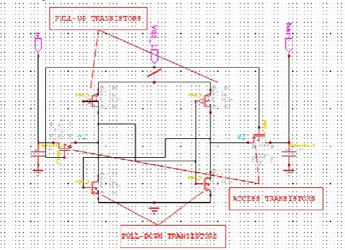
In the basic SRAM cell two NMOS access transistors, two pull-up transistors and two pull-down transistors, six in all are used as shown in schematic of Fig. 2.
Fig. 2: Schematic Designing of Standard 6T SRAM
ISSN(Online): 2319-8753 ISSN (Print): 2347-6710
I
nternational
J
ournal of
I
nnovative
R
esearch in
S
cience,
E
ngineering and
T
echnology
(A High Impact Factor, Monthly, Peer Reviewed Journal) Visit: www.ijirset.com
Vol. 8, Issue 8, August 2019
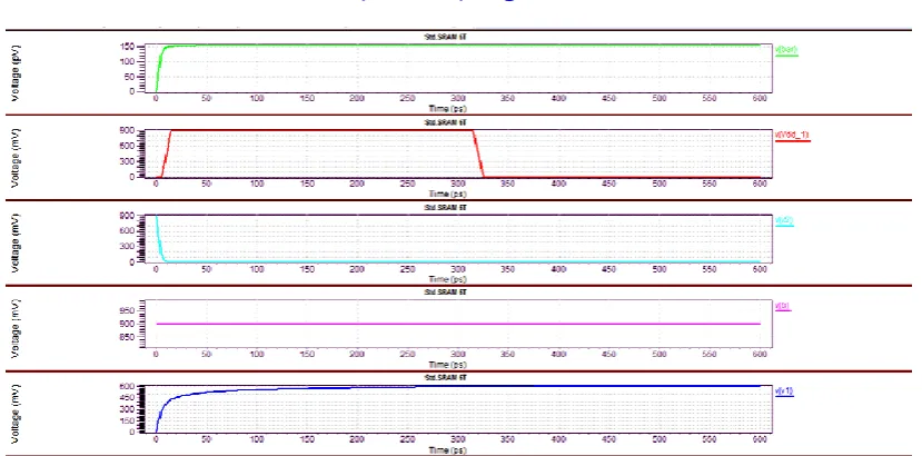
Fig. 3: Waveforms of Standard 6T SRAM
Here the description of all the signals is as follows:
Vdd_1- Write Enable Signal
b- Bit Line Signal
bar- Inverted Bit Line Signal
v1- Internal Node corresponding to Bit Line
v2- Internal Node corresponding to Inverted Bit Line
As soon as all the initial conditions (b, bar, v1, v2) and Write Enable clock signal Vdd-1 are activated, SRAM overwrite operation (Sec. 4.1) causes the transition of node voltages to their inverted logic values. So the voltage waveforms of v1 and v2 make transition from low to high and high to low respectively. Nodes will retain these values until the next write clock pulse arrived.
IV. RESULTS AND PERFORMANCE ANALYSIS
Here we will show the results obtained after simulation and then analyze the performance on the basis of these results first for power and delay then for area.
Power and Delay
ISSN(Online): 2319-8753 ISSN (Print): 2347-6710
I
nternational
J
ournal of
I
nnovative
R
esearch in
S
cience,
E
ngineering and
T
echnology
(A High Impact Factor, Monthly, Peer Reviewed Journal) Visit: www.ijirset.com
Vol. 8, Issue 8, August 2019
Table1: Simulation Results for Memory Overwrite
Configuration Additional Power(nw) Delay (ps) Power- Delay Product(nws) Transistors Signals
6T 0 0 871.74 6.76 5.89 VGn 1 1 720.85 6.23 4.49 VVn 1 1 685.97 7.91 5.43 VGVn 2 2 646.40 7.44 4.81 8T 2 1 912.02 6.82 6.22 VGc 3 2 766.16 6.01 4.60 VVc 3 2 776.45 6.89 5.34 VGVc 4 3 698.23 6.53 4.56
As all results are carried out for 16nm predictive technology power and delay shows a remarkable reduction in outputs than their predecessor technologies also the results given in Table 1
V. CONCLUSION
Accessing SRAM involves either storing data to the memory cells (writing) or retrieving previously stored data (reading). The focus of this chapter was writing to memory. First, a description of the write process was given. The problems with its operation were then revealed: three short circuits responsible for significant power losses were identified and causes for delay were mentioned. To remove the short circuits, the addition of virtual source transistor(s) to the standard 6T differential memory cell was proposed. Delay was intended to be reduced by exchanging the two nMOS access transistors for two CMOS transmission gates. Seven different variations of the 6T memory cell were then designed using different combinations of virtual source transistors and transmission gates. Finally, each design was tested through simulation and its performance was evaluated. But most importantly processing with 16nm technology itself is a big advantage which caused shrinking dimensions of the transistor so very small size of memory cell(of the order of n2m2), very low power(<1uw) required for reliable operation of both switching and storage operations, while at the same time also increasing the speed of operation(<10ps) of the device.
REFERENCES
[1] Anie Jain and Shyam Akashe, “Optimization of Low Power 7T SRAM Cell in 45nm Technology”, Advanced Computing & Communication Technologies (ACCT), Jan. 2012, pp. 324-327.
[2] David Hentrich, Erdal Oruklu and Jafar Saniie, “Performance evaluation of SRAM cells in 22nm predictive CMOS technology”, Electro/Information Technology (EIT), June 2009, pp. 470-475.
[3] Prashant Upadhyay, Mr. Rajesh Mehra, Niveditta Thakur, “Low power design of an SRAM cell for portable devices”, Computer and Communication Technology (ICCCT), Sept. 2010, pp. 255-259. [4] H.P Rajani, Hansraj Guhilot and S.Y Kulkanri, “Novel stable sram for ultra low power deep submicron cache memories”, Recent Advances in Intelligent Computational Systems (RAICS), Sept. 2011, pp. 489-492.
[5] Hiroaki Okuyama, Takeshi Nakano, Shuichi Nishida, Etsuro Aono. Hisahiro Satoh and Shigeru Akita, “A7.5-ns 32Kx8 CMOS SRAM”, IEEE Journal of solid-state circuits, vol. 23, no. 5, Oct. 1988.
[6] Masaya Sumita, Shiro Sakiyama, Masayoshi Kinoshita, Yuta Araki, Yuichiro Ikeda, and Kohei Fukuoka., “Mixed body bias techniques with Fixed Vt and Ids Generation Circuits”, IEEE Journal of solid-state circuits, vol. 40, no. 1, Jan. 2005.
[7] Budhaditya Majumdar and Suman Basu, “Low power single bitline 6T SRAM cell with high read stability”, Recent Trends in Information Systems (ReTIS), Dec.2011, pp. 169-174.
ISSN(Online): 2319-8753 ISSN (Print): 2347-6710
I
nternational
J
ournal of
I
nnovative
R
esearch in
S
cience,
E
ngineering and
T
echnology
(A High Impact Factor, Monthly, Peer Reviewed Journal) Visit: www.ijirset.com
Vol. 8, Issue 8, August 2019
[9] Shin-Pao Cheng and Shi-Yu Huang, “A Low-Power SRAM Design Using Quiet-Bitline Architecture”, Proceedings of the 2005 IEEE International Workshop on Memory Technology, Design, and Testing, 2005.
[10] Hong Zhu and Volkan Kursun, “Application-specific selection of 6T SRAM cells offering superior performance and quality with a triple-threshold-voltage CMOS technology”, Quality Electronic Design (ASQED), July 2011, pp. 68-73.
[11] Zhiyuan Yu, Yinhui Chen, Haiqing Nan, Wei Wang and Ken Choi, “Design of a novel low power 6-T CNFET SRAM cell working in sub-threshold region”, Electro/Information Technology (EIT), May 2011, pp. 1-5.
[12] Hirdaya Narain Mishra and Yashwanta Kumar Patel, “Design, simulation and characterization of memory cell array for low power SRAM using 90nm CMOS technology”, Power, Control and Embedded Systems (ICPCES), Dec. 2010, pp. 1-3.
[13] Kong Zhi Hui and Do Anh Tuan, “A 16Kb 10T-SRAM with 4x read-power reduction”, Circuits and Systems (ISCAS), June 2010, pp. 3485-3488.