Design of 32-bit Carry Select Adder with Reduced Area
Yamini Devi Ykuntam
Department of ECEGMRIT Rajam-532127, India
M.V.Nageswara Rao
Department of ECEGMRIT Rajam-532127, India
G.R.Locharla
Department of ECEGMRIT Rajam-532127, India
ABSTRACT
Addition is the heart of arithmetic unit and the arithmetic unit is often the work horse of a computational circuit.So adders play a key role in designing an arithmetic unit and also many digital integrated circuits. Carry Select Adder (CSLA) is one of the fastest adders used in many data processors and in
digital circuits to perform arithmetic operations.But CSLA is
area-consuming because it consists of dual ripple carry adder (RCA) in the structure. To reduce the area of CSLA, a CSLA with Binary to Excess-1 Converter is already designed which reduces the area of adder. But there are other techniques to design a CSLA to reduce its area. One of such technique is using an add one circuit technique. This paper proposes the design of square root CSLA (SQRT CSLA) using add one circuit with significant reduction in area. The proposed design is synthesized using Leonardo Spectrum to get area (number of gates) and delay (ns). The performance in terms of area and delay are evaluated for square root CSLA using add one circuit and are compared with existing SQRT CSLA and SQRT CSLA using Binary to Excess-1 Converter (BEC). The results analysis shows that the proposed SQRT CSLA using add one circuit is better than the existing SQRT CSLA and SQRT CSLA using BEC.
Keywords
SQRT CSLA, ASIC, BEC, add one circuit, ISIM , Leonardo Spectrum
1.
INTRODUCTION
VLSI IC’s are those circuits which contain more than 105
transistors and these circuits can be used as general purpose IC’s such as microprocessors, memories, DSPs and also as Application Specific IC’s (ASICs). In VLSI technology, the main design entity is area which measures the cost and power consumption of an IC. Reduced area and high speed data path logic systems are the main areas of research in VLSI system [1].
High-speed addition and multiplication has always been a fundamental requirement of high-performance processors and systems. The speed of addition and multiplication operations depends on the speed of the adder on which the operations are performed. There are many types of digital adders are available for designing a digital circuits and arithmetic units in a processor. The performance of digital adders is limited by the speed of addition. The reason behind this limitation is the time taken to propagate the carry. The sum for each bit in an elementary adder is generated sequentially only after the previous bit position has been summed and a carry propagated into the next position [2].
There are many ways to design an adder. The Ripple Carry Adder (RCA) structure is chain of Full adders which is easy to design, but takes longer time to perform addition operation due to the delay in propagation of carry from one adder to
another. The delay due to carry propagation in RCA is proportional to the number of input bits (N) to RCA. For large values of N, the delay of the RCA also increases. To overcome delay problem, a new adder structure is designed called Carry Look-Ahead Adder (CLA).
CLA is designed using two blocks namely propagate and generate block. As the number of input bits increases, the size of propagate and generate blocks also increases which causes increase in area and also introduces delay again. So CLA avoids the delay problem for less number of input bits, but not suitable for large size input. The CSLA provides a compromise between RCA and CLA.
The CSLA is used in many digital systems to improve the carry propagation delay by independently performing addition
operation using two RCAs by assuming Cin for one RCA as 0
and for other as 1 [3], [4]. And the final sum is chosen in between the two results of RCA with the help of a multiplexer (mux) to which the control signal is carry out of previous adder stage. Due to the use of two RCAs, the area of CSLA increases. To reduce the area, the RCA with Cin=1 are
replaced with add one circuit.The SQRT CSLA has been chosen for comparison with the proposed design as it has a more balanced delay, and requires lower power and area [5-6]. The 8-bit, 16-bit, 32-bit SQRT CSLA using add one circuit is proposed to minimize the area and power.
This paper in brief is structured as follows-section 2 describes about conventional SQRT CSLA and its delay, area evaluations. Section 3 describes about existing SQRT CSLA with BEC and its area, delay evaluation. Section 4 describes about proposed SQRT CSLA with add one circuit and its area, delay evaluation. Section 5 explains the synthesis results of the proposed adder structure and its comparison with the other two adder structure. Finally this paper ends with conclusion.
2.
SQUARE ROOT CARRY SELECT
ADDER
2.1
Structure of SQRT CSLA
The CSLA is used in many digital systems design to overcome the problem of carry propagation delay by independently performing addition operation by considering
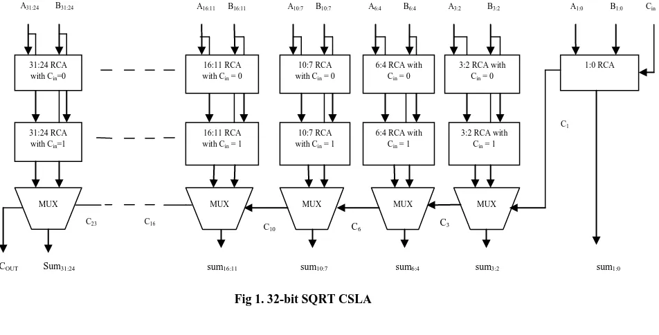
carry inputs (Cin) as 1 and 0. Figure 1. shows a 32-bit SQRT
CSLA. The SQRT CSLA is divided into m=√2m carry select stages (CSS), where m is number of input bits. The 32 bit SQRT CSLA consists of 7 CSS. The CSS consists of two ripple carry adders one with carry in 0 and other with carry in 1. It also consists of a multiplexer which is used to select the sum and carry values from the two RCAs by using the control signal to it. The control signal to multiplexer is nothing but the carry out of the previous CSS. If the control signal is 1
then sum and carry out of RCA with Cin=1 is selected by the
2.2
Delay and area evaluation of basic
modules in SQRT CSLA
Basic modules in CSLA are Ripple Carry Adder (RCA) and multiplexer (mux). RCA is composed of full adder (FA) and half adder (HA). The full adder consists of two AND gates, one OR gate and two XOR gates. In turn the XOR gate is formed by two inverters, two AND gates and one OR gate, totally XOR gate is composed of 5 gates. So FA consists of 13 gates. The half adder consists of one AND gate and one XOR gate, so HA consists of totally 6 gates. The mux used is 2:1 mux is used. It consists of one inverter, two AND gates and one OR gate. Therefore 2:1 mux consists of 4 gates. While evaluating the delay and area , it is considered that all gates to be made up of AND, OR, and Inverter (AOI).The delay of each gate equal to 1 unit and also area of each equal to 1 unit. The maximum delay can be calculated by adding up the number of gates in the longest path. The area evaluation is done by counting the total number of AOI gates present in each logic block.
Table 1. Delay and area count of basic modules of CSLA
Basic modules Delay Area
XOR 3 5
2:1 Mux 3 4
Full adder 6 13
Half adder 3 6
2.3
Delay and area evaluation of SQRT
CSLA
As shown in fig.1, group2 consists of a 2-bit RCA with Cin=0,
a 2-bit RCA with Cin=1 and also a 6:3 Mux. The 2-bit RCA
with Cin=0 consists of one FA and one HA where as 2-bit
RCA with Cin=1consists of two FAs. Based on the area count
of table-1, the total number of gates present in group2 is:
Gate count = 57 (FA + HA + MUX)
FA = 39(3*13)
HA = 6(1*6)
Mux = 12(3*4)
The total number of gates present in the remaining groups can
be calculated in the same way as for group 2. The maximum
delay can be calculated by adding the delays of gates in the longest path in the architecture that contributes the maximum delay. In this adder, dual RCAs are used which occupies more area which in turn increases the power consumption. So a new adder is proposed in [7] is SQRT CSLA with Binary to Excess-1 Converter (BEC).
3. EXISTING STRUCTURE
3.1 SQRT CSLA with BEC
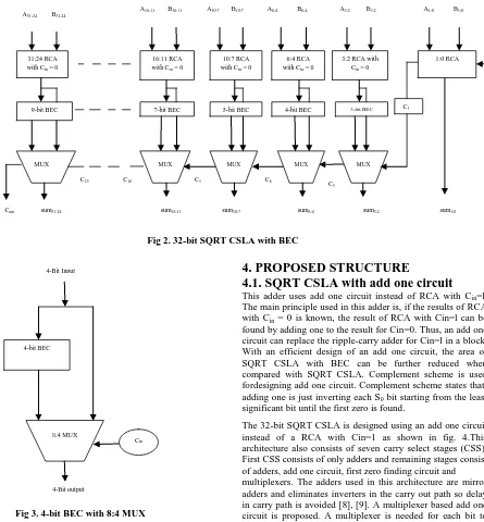
To reduce the area and power consumption of the regular CSLA, RCA with Cin =1 is replaced with BEC (Binary to
Excess-1 Converter) [7] as shown in fig 2. An n-bit RCA, can be replaced with a n+1-bit BEC. Figure 3. explains the basic function of the CSLA by using the 4-bit BEC together with the mux. A set of four bits (bit input) and the other set of 4-bits (4-bit BEC output) were given as input to the 8:4 multiplexer. Depending on the control signal Cin, either the
BEC output or the 4-bit input. The advantage of the BEC logic in SQRT CSLA is that, as the number of input bits is increased the requirement of area is progressively decreased. Figure 2. shows the structure of a 32-bit SQRT CSLA with BEC.
3.2. Delay and area evaluation of SQRT
CSLA with BEC
As shown in fig. 2, group2 consists of a 2 bit RCA with Cin=0,
a 3-bit BEC and a 6:3 Mux. The 2-bit RCA with Cin=0
consists of a FA and HA. Based on the area count of table-1, the total number of gates present in group2 is:
C1
[image:2.595.85.561.75.317.2]C16
Fig 1. 32-bit SQRT CSLA
C6 C3
C23
3
31:24 RCA with Cin=0
31:24 RCA with Cin=1 A31:24 B31:24
MUX
18:9
COUT Sum31:24
C16
C10
1
A16:11 B16:11 A10:7 B10:7 A6:4 B6:4 A3:2 B3:2 A1:0 B1:0 Cin
sum16:11 sum10:7 sum6:4 sum3:2 sum1:0
MUX
10:5
MUX
8:4
MUX
6:3 10:7 RCA
with Cin = 0
6:4 RCA with Cin = 0
3:2 RCA with Cin = 0
1:0 RCA
16:11 RCA with Cin = 1
10:7 RCA with Cin = 1
6:4 RCA with Cin = 1
3:2 RCA with Cin = 1
MUX
Fig 3. 4-bit BEC with 8:4 MUX
Gate count =43(FA+HA+MUX+BEC) FA = 13(1*13)
HA = 6(1*6) AND=1 NOT=1 XOR=10(2*5) Mux = 12(3*4)
The total number of gates present in the remaining groups can
be calculated in the same way as for group 2.The maximum
delay can be calculated by adding the delays of gates in the longest path in the architecture that contributes the maximum delay. But delay is increased in this architecture. To reduce this delay penalty, anew architecture of SQRT CSLA using add one circuit is proposed.
4. PROPOSED STRUCTURE
4.1. SQRT CSLA with add one circuit
This adder uses add one circuit instead of RCA with Cin=l.The main principle used in this adder is, if the results of RCA with Cin = 0 is known, the result of RCA with Cin=l can be
found by adding one to the result for Cin=0. Thus, an add one circuit can replace the ripple-carry adder for Cin=l in a block. With an efficient design of an add one circuit, the area of SQRT CSLA with BEC can be further reduced when compared with SQRT CSLA. Complement scheme is used fordesigning add one circuit. Complement scheme states that, adding one is just inverting each S0 bit starting from the least
significant bit until the first zero is found.
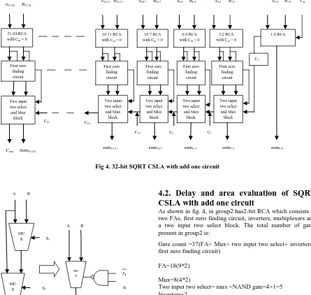
The 32-bit SQRT CSLA is designed using an add one circuit instead of a RCA with Cin=1 as shown in fig. 4.This architecture also consists of seven carry select stages (CSS). First CSS consists of only adders and remaining stages consist of adders, add one circuit, first zero finding circuit and multiplexers. The adders used in this architecture are mirror adders and eliminates inverters in the carry out path so delay in carry path is avoided [8], [9]. A multiplexer based add one circuit is proposed. A multiplexer is needed for each bit to choose in between sum and complement of sum.
The control signal of the multiplexer is from the first zero finding circuit. The first zero finding circuit is NMOS and PMOS chains. This circuit generates 0 at the kth node if no zero is founded until kth bit from the least significant bit; otherwise, it generates 1. If the control signal is 0, the multiplexer chooses sum otherwise, it chooses the inverted sum. The least significant bit does not need a multiplexer since S10 is always the opposite of S
0
0. This saves a few
transistors for each block
8:4 MUX 4-bit BEC
Cin 4-Bit Input
4-Bit output
Cout sum31:24 sum16:11 sum10:7 sum6:4 sum3:2 sum1:0 31:24 RCA
with Cin = 0
9-bit BEC
MUX A31:24 B31:24
C23 C16
C1
C10 C6 C3
A16:11 B16:11 A10:7 B10:7 A6:4 B6:4 A3:2 B3:2 A1:0 B1:0 Cin
C3 7-bit BEC 5-bit BEC 4-bit BEC 3-bit BEC
MUX MUX MUX MUX
16:11 RCA with Cin = 0
10:7 RCA with Cin = 0
6:4 RCA with Cin = 0
3:2 RCA with Cin = 0
1:0 RCA
C1 0
[image:3.595.100.546.75.290.2]Fig 5. Replacing two multiplexers by one multiplexer with a NAND.
The carry out for a block can be chosen between the carry out for the RCA or the carry out for the add-one circuit. Finally, the multiplexers is placed in the bottom to choose between the results for Cin=0 and the results for Cin=l. A twoinput two select block is used to replace the two multiplexers with one multiplexer and a NAND can replace the two multiplexers as shown in fig. 5.
Since the sum of the most significant bit for Cin=0 is used to
get the carryout of a block, the proposed CSA delay is longer than the CSA using dual RCAs. Therefore, by replacing the last FA by two-level XORs to get the sum faster, the delay time can be reduced.
4.2. Delay and area evaluation of SQRT
CSLA with add one circuit
As shown in fig. 4, in group2 has2-bit RCA which consists of two FAs, first zero finding circuit, inverters, multiplexers and a two input two select block. The total number of gates present in group2 is:
Gate count =37(FA+ Mux+ two input two select+ inverters+ first zero finding circuit)
FA=18(9*2)
Mux=8(4*2)
Two input two select= mux +NAND gate=4+1=5 Inverters=2
First zero finding circuit=4
The total number of gates present in the remaining groups can be calculated in the same way as for group 2. The maximum delay can be calculated by adding the delays of gates in the longest path in the architecture that contributes the maximum delay.
Table 2. Comparison of area of three adder structures (theoretical calculated results)
Group Basic SQRT
CSLA area
SQRT CSLA with BEC
area
SQRT CSLA with add one circuit area
Group 1 26 26 19
Group 2 57 43 35
Group 3 87 66 54
Group 4 117 89 71
Group 5 147 112 86
total 434 336 265
Fig 4. 32-bit SQRT CSLA with add one circuit
C1
Two input two select and Mux block
C23 C 16
A16:11 B16:11 A10:7 B10:7 A6:4 B6:4 A3:2 B3:2 A1:0 B1:0 Cin
31:24 RCA with Cin = 0
First zero finding circuit
A31:24 B31:24
Cout Sum31:24
First zero finding
circuit 10:7 RCA
with Cin = 0
6:4 RCA with Cin = 0
3:2 RCA with Cin = 0
1:0 RCA
sum15:11 sum10:7 sum6:4 sum3:2 sum1:0 First zero
finding circuit
First zero finding
circuit
First zero finding circuit
Two input two select and Mux block
Two input two select and Mux block
Two input two select and Mux block
Two input two select and Mux block
C3 C6
C10
0
16:11 RCA with Cin = 0
O MU
X
MU X
A B
S1
S2
O
1 S
S2 MU
[image:4.595.313.548.608.750.2]By comparing the area of proposed SQRT CSLA with the basic CSLA and SQRT CSLA with BEC in table 2, it is clear that the proposed adder structure has 169 less gates when compared with basic SQRT CSLA structure and 71 less gates when compared with SQRT CSLA with BEC. For further evaluation of the performance in terms of area and delay, the three adder structures must be designed using VHDL, than simulated and synthesized for ASIC implementation.
5. SIMULATED RESULTS AND
COMPARISON
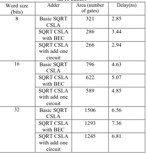
[image:5.595.51.288.305.554.2]The adders design proposed in this paper has been developed using VHDL and all the simulations are carried outusing ISim simulator. The designs are synthesized in Leonardo Spectrum to get the area (number of gates) and delay (ns). The area and delay required for the traditional CSLA and SQRT CSLA with BEC logic are calculated and compared with the proposed SQRT CSLA with add one circuit. The area and delay of three synthesized adders in Leonardo Spectrum for word size length 8bit, 16bit and 32bit is illustrated in Table-3.
Table 3. Comparison of area and delay in between the three adders
Word size (bits)
Adder Area (number of gates)
Delay(ns)
8 Basic SQRT
CSLA
321 2.85
SQRT CSLA with BEC
286 3.44
SQRT CSLA with add one
circuit
266 2.94
16 Basic SQRT
CSLA
796 4.63
SQRT CSLA with BEC
622 5.07
SQRT CSLA with add one
circuit
589 4.85
32 Basic SQRT
CSLA
1506 6.56
SQRT CSLA with BEC
1293 7.36
SQRT CSLA with add one
circuit
1245 6.81
6. CONCLUSION
The area and delay of 8-bit, 16-bit, 32-bit and 64-bitbasic SQRT CSLA, SQRT CSLA with BEC logic are evaluated and compared with the proposed SQRT CSLA with add one circuit logic. It is clear from table-3 that, the proposed adder takes less delay and area when compared with SQRT CSLA with BEC logic. It is also observed that in the proposed adder the reduction in area is very high with insignificant penalty in the delay when compared with traditional SQRT CSLA. As the input length is progressed, the area is decreased in the same proportion, but in the same proportion the delay penalty is not increased. Since the area in the proposed adder is very less, it is obvious that, the power consumption is also very less. Therefore this adder can be preferred for low power applications.
7. REFERENCES
[1] O. J. Bedrij, “Carry-select adder,” IRE Trans. Electron. Comput.,pp.340–344, 1962.
[2] Y. Kim and L.-S. Kim, “64-bit carry-select adder with reduced area,”Electron. Lett., vol. 37, no. 10, pp. 614– 615, May 2001.
[3] B. Ramkumar, H.M. Kittur, and P. M. Kannan, “ASIC implementation of modified faster carry save adder,” Eur. J. Sci. Res., vol. 42, no. 1, pp. 53–58, 2010. [4] T. Y. Ceiang and M. J. Hsiao, “Carry-select adder using
single ripple carry adder,” Electron. Lett., vol. 34, no. 22, pp. 2101–2103, Oct. 1998.
[5] J. M. Rabaey, Digtal Integrated Circuits—A Design Perspective. Upper Saddle River, NJ: Prentice-Hall, 2001.
[6] Y. He, C. H. Chang, and J. Gu, “An area efficient 64-bit square root carry-select adder for low power applications,” in Proc. IEEE Int. Symp. Circuits Syst., 2005, vol. 4, pp. 4082–4085.
[7] B. Ramkumar and Harish M Kittur, “Low-Power and Area-Efficient Carry Select Adder” IEEE transactions on very large scale integration (VLSI) systems, vol. 20, no. 2, February 2012]
[8] N. Weste and K. Eshragian, Principles of CMOS VLSI Designs: A System Perspective, 2nd ed., Addison-Wesley, 1985-1993.