Static-Noise-Margin Analysis of Conventional 6T SRAM
Cell at 45nm Technology
Nahid Rahman
Department of electronics and communication FET-MITS (Deemed university), Lakshmangarh,
India
B. P. Singh
Department of electronics and communication FET-MITS (Deemed university),Lakshmangarh,
India
ABSTRACT
Static random access memory (SRAM) is a type of volatile semiconductor memory to store binary logic '1' and '0'. The SRAM sizing has been scaled down due to the increase density of SRAM in System-On-Chip (SoC) and other integrated devices, which works on lower supply voltage. This leads to considerable amount of power saving, but the stability and performance of the SRAM circuit is also being affected due to the scaling of supply voltage. The lower supply voltage reduces the Static Noise Margin upon which the stability of the SRAM cell depends. With lower Vdd, the delay of SRAM cell increases considerably and speed of the SRAM will be lowered. This paper discusses about the noise effect on Read SNM and Write SNM of Conventional 6T SRAM cell. This paper also presents the effect of device parameters on Conventional 6T SRAM cell which increases the cell stability without increasing transistor count at 45nm technology.
General Terms
CMOS logic,SRAM and VLSI.
Keywords
Static Noise Margin (SNM) and Stability.
1.
INTRODUCTION
SRAM uses bi-stable latching circuitry made of Transistors/MOSFETS to store each bit. Compared to Dynamic Random access memory (DRAM), SRAM doesn’t have a capacitor to store the data, hence SRAM works without refreshing. In SRAM the data is lost when the memory is not electrically powered. Advances in chip design using CMOS technology have made possible the design of chips for higher integration, faster performance, and lower power consumption. To achieve these objectives, the feature size of CMOS devices has been dramatically scaled to smaller dimensions over the last few years. Power consumption of SRAMs account for a significant portion of the overall chip power consumption and due to high density, low power operation is a feature that has become a necessity in today’s microprocessors.
Hence, power consumption of SRAM modules must be reduced and has been under extensive investigation in the technical literature. The most effective approaches to meet this objective is to design SRAM cells whose operation is ultra-low power. Recent published works have shown that the Conventional 6T SRAM suffers severe stability degradation due to access disturbance at low–power mode. The goal of this paper is to determine the effect of several circuit parameters on the SNM of 6T SRAM Cell designed in 45nm process technology.
2.
CONVENTIONAL 6T SRAM CELL
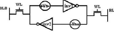
The conventional 6T memory cell comprised of two CMOS invertors cross coupled with two pass transistors connected to a complimentary bit lines as shown in Figure 1. The gate of access transistors N3 and N4 are connected to the WL (word line) to have data written to the memory cell or read from the memory cell through the BL or BLB (bitlines) during write and read operation. [image:1.595.317.555.360.558.2]The bit lines act as I/O buses which carry the data from the memory cell to the sense amplifier. Although it is not necessary to have two bit lines, both the signal and its inverse are typically provided in order to improve noise margins. SRAM cell perform three different operations, read, write and hold operation.
Fig 1: Conventional 6T SRAM Cell
3.
STATIC-NOISE-MARGIN (SNM)
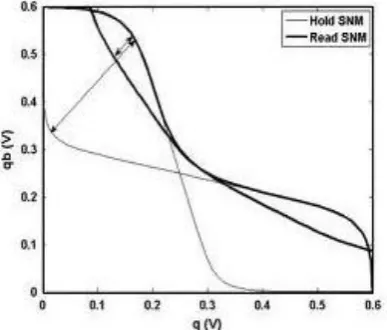
The stability of SRAM circuit depends on the Static Noise Margin. A basic SNM is obtained by drawing and mirroring the inverter characteristics and finding the maximum possible square between them. This is a graphical technique of estimating the SNM [1]. [image:1.595.330.525.683.739.2]Figure 2 shows a common way of representing the SNM graphically for a bit-cell holding data. It plots the Voltage Transfer Characteristic (VTC) of Inverter 2 (inv2) and the inverse VTC-1 from Inverter 1(inv1). The resulting two-lobed curve is called a “butterfly curve” and is used to determine the SNM. The SNM is defined as the length of the side of the largest square that can be embedded inside the lobes of the butterfly curve.
Consider the case when the value of the noise sources with value Vn are introduced at each of the internal nodes in the bit cell. When the value of Vn increases from 0, this causes the VTC-1 for first inverter in Figure 2 to move downward and the VTC for the second inverter to move to the right. Once both move by the SNM value, the curves meet at only two points [3].
Fig 3: General SNM characteristics during Standby and Read operation
The resulting two-lobed curve is called as a “butterfly curve” as shown in Figure 3 and is used to determine the SNM. Values of SNM vary in different operation mode. SNM is becoming important factor to check the stability during read operation. It’s visible in the Fig. 3 that during read operation, the SNM takes its lowest value and the cell is in its weakest state.
The SRAM cell immunity to static noise is measured in terms of SNM that quantifies the maximum amount of voltage noise that can be tolerated at the cross-inverters output nodes without flipping the cell [4]. Any change in the noise, changes the value of the SNM during cell operation. Though the SNM is important during hold, cell stability during active operation represents a more significant limitation to SRAM operation.
4. STABILITY PROBLEM IN 6T SRAM
The conventional 6T-cell schematic is shown in Figure 4. This most commonly used SRAM cell implementation has the advantage of very less area [5]. [image:2.595.321.543.72.244.2]However, the potential stability problem of this design arises during read and writes operation, where the cell is most vulnerable towards noise and thus the stability of the cell is affected. If the cell structure is not designed properly, it may change its state during read and write operation. There are two types of noise margin which affects the Cell stability that are discussed shortly.
Fig 4: Voltage Stability Problem of 6T SRAM Cell
4.1 Read Static-Noise-Margin
During read accesses, the Read-SNM decreases [8]. This is due to the reason that Read-SNM is calculated when the word line is set high and both bit line are still precharged high. At the onset of a read access, the access transistor (WL) is set to “1” and the bit-lines are already precharged to “1”.The internal node of the bit-cell representing a zero gets pulled upward through the access transistor due to the voltage dividing effect across the access transistor and drive transistor. This increase in voltage severely degrades the SNM during the read operation as shown in the Figure 3.
During the read operation, a stored “0” can be overwritten by a “1” when the voltage at node V1 reaches the Vth of nMOS
N1 to pull node V2 down to “0” and in turn pull node V1 up even further to “1” due to the mechanism of positive feedback. This results in wrong data being read or a destructive read when the cell changes state [7].
4.2 Write Static-Noise-Margin
The write noise margin is defined as the minimum bitline voltage needed to flip the state of cell. During a write operation, the input data are sent to the bitlines, and then the word lines are activated to access the cell. The bitline that is charged to ‘0’ pulls the node of the cell storing ‘1’ to ‘0’ causing the cell to flip state. Since the cross-coupled inverters have complementary data, their VTCs are measured using different circuits. The circuit that represents the inverter with ‘1’ at its output and its bitline is connected to GND to simulate a write ‘0’ to that node. A DC voltage sweep is applied at node V1 and the voltage output at node V2 is measured, when the bitline( BL) is connected to GND and wordline (WL) is charged to Vdd.
5. EFFECT OF DEVICE PARAMETERS
ON SNM OF SRAM CELL
[image:2.595.72.266.238.403.2]Due to the need of battery operated device, the scaling in CMOS technology continues. So there is a modification of 6T SRAM cell to attain the optimum cell stability by modifying supply voltage, cell ratio, pull-up ratio and temperature and word line voltage modulation. These modifications show a drastic change in the static noise margin curves [9].
5.1 Supply Voltage Modulation Effect
The effect of power supply modulation is important parameter which changes the cell stability during read mode and has been widely acceptable. It is preferable that the supply voltage must be maximum for increase SNM and also for cell stability.
For this analysis, the supply voltage is varied from 0.4V to 1V. The noise margin for all operation is proportional to the supply voltage. Voltage scaling limits the level such that noise margin is still greater than the expected noise margin. The effect of decreasing supply voltage on Read SNM and Write SNM is as shown in Figure 5 (a) and (b).
.
Fig 5(a): Effect on supply Voltage on Read SNM
Figure 5(b): Effect on supply Voltage on Write SNM
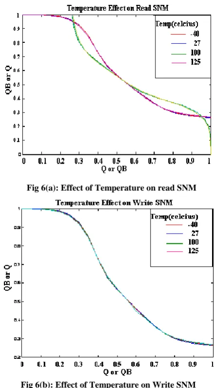
5.2 Temperature Modulation Effect
The effect of temperature on the noise margin is almost insignificant as shown by the results summarized in Figure 6 at temperatures -40°C, 27°C, 100°C and 125°C.
Fig 6(a): Effect of Temperature on read SNM
Fig 6(b): Effect of Temperature on Write SNM
There is no change in noise margin by varying the temperatures. Thus the stability of SRAM Cell is not hindered by the change in temperature. So the variation in temperature hardly affects the Read SNM and Write SNM as shown in Figure 6 (a) and (b).
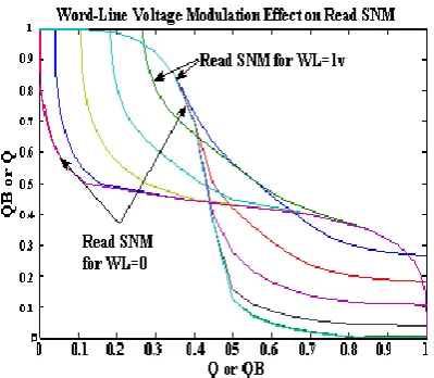
5.3 Word-Line Voltage Modulation Effect
[image:3.595.317.537.135.534.2] [image:3.595.52.284.311.744.2]Fig 7(a): Effect of Wordline Voltage Modulation on Read SNM
Fig 7(b): Effect of Wordline Voltage modulation on Write SNM
Reducing the effective word-line voltage could provide an interesting technique to improve the stability of the cell during read and write operations. As we approach to zero Word-line voltage, the SNM is maximum. The reason behind maximum SNM is that, at WL=0, the SRAM is in standby mode and static noise margin is maximum at hold operation as already seen in Figure 3.
5.4 Transistor Width Modulation Effect
The Read and Write Static Noise Margin of 6T SRAM cell is affected by the transistor width modulation. The proper sizing of Driver transistor is responsible for a drastic change in the value of SNM. The Cell Ratio and Pull up Ratio affects the stability of the SRAM Cell.
5.4.1 Cell Ratio
Cell ratio is defined as ratio between the sizes of the driver (pull down) transistor to the size of access transistor Eq.(1):
CR(r) = Size of pull down transistor (1) Size of access transistor
The cell ratio affects the stability of SRAM Cell during read operation. The read noise margin, increases with increasing the cell ratio.
To keep cell area within reasonable values, we restrict the values of Cell ratio (r) and p
[image:4.595.70.270.69.243.2]minimum, 1, and a maximum of 2.5, (i.e. rmax = qmax = 2.5).
Table 1. Cell Ratio verses Read SNM.
Technology
(nm) CR(r) READ SNM
(mV)
45nm
1.0 70
1.5 131
2.0 150
2.5 161
[image:4.595.317.540.200.296.2]It can be seen in Table 1, that as we increase the Cell ratio, the Read SNM is increased to a greater extent resulting into increased stability of the SRAM Cell.
Fig 8: Effect of Cell Ratio on Read SNM
The larger the cell ratio, the larger the pull down network which means that the node storing 0 is more robust against noise introduced by the bitline precharged voltage during read. The node voltage retains its value because of the strong pull down network. In Figure 8, the Cell Ratio is varied as 1, 1.5, 2 and 2.5. Thus the Read SNM is minimum during CR=1 and maximum when CR=2.5.
5.4.2 Pull up Ratio
Pull up ratio is nothing but a ratio between sizes of the load transistor (pull up) to the size of access transistor as shown in Eq.(2)
PR(q) = Size of pull up transistor (2) Size of access transistor
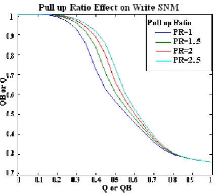
[image:4.595.63.272.280.474.2] [image:4.595.319.536.330.524.2]transistors whose size ratio defines the pull-up ratio. The bitline pulled to GND pulls the node storing ‘1’ to GND to flip the state.
[image:5.595.63.277.195.386.2]The strength of the pull-up transistor determines the difficulty of writing data or flipping the state of cell. With increased pull-up ratio, it is more difficult to write or pull the node to GND and hence the write margin and write trip voltage is decreased. Thus increasing the pull up ratio during write is of no good as it increases the difficulty in writing data into the SRAM Cell.
Fig 9: Effect of Pull up Ratio on Write SNM
Figure 9 depicts the effect of pull up ratio which is varied from 1 to 2.5. The increase in pull up ratio decreases the ease with which the data is written in the SRAM Cell and thus the Write SNM decreases.
6. CONCLUSION
The simulation results, discussed above improve the Read SNM and Write SNM of Conventional 6T SRAM Cell. The higher SNM can be achieved by modifying the device parameters of conventional 6T SRAM cell without requiring any modification of the SRAM cell array design. The Modified 6T can be used as a cache memory in internal CPU. It also maintains its Read-SNM at higher temperature range, thus it can be used in Industry and Military purposes also. So to overcome the SNM problem encountered with conventional
6T SRAM cell and to avoid the area overhead occurred due to additional transistors, we have proposed a method of introducing the effect of device parameters for improving the Static-Noise-margin of Conventional 6T SRAM Cell.
7. ACKNOWLEDGMENTS
The authors are very thankful to MITS (Deemed University) for providing a good laboratory facility. We simulate the result on Tanner EDA Tool version 12.6.
8. REFERENCES
[1] E. Seevinck et al., “Static-Noise Margin Analysis of MOS SRAM Cells,” IEEE J.Solid-State Circuits, vol.SC-22, no.5 pp.748-754, Oct. 1987.
[2] E. Grossar “Read Stability and Write-Ability Analysis of SRAM Cells for Nanometer Technologies”, IEEE J.Solid-State Circuits,vol.41,no.11 ,pp. 2577-2588,Nov. 2006.
[3] Benton H. Calhaun, Anantha P. Chandrakasan “Static Noise Margin Variation for Sub-threshold SRAM in 65 nm CMOS”, IEEE Journal of Solid-State Circuits,, pp.1673-1679. vol.41,July 2006.
[4] Benton H. Calhoun Anantha P. Chandrakasan, “Analyzing Static Noise Margin for Sub-threshold SRAM in 65nmCMOS”,ESSCIRC,2005.
[5] K. Takeda et al., “A Read-Static-Noise-Margin- Free SRAM Cell for Low-VDD and High-Speed Applications,” IEEE J.Solid-State Circuits,vol.41, no.1 pp.113-121, Jan., 2006.
[6] Do Anh-Tuan et al., “A 8T Diffrential SRAM With Improved Noise Margin for Bit-Interleaving in 65nm CMOS,” IEEE transactions on circuits and systems, vol.58, no.6,pp.1252-1263, June 2011.
[7] S.Birla et a.l.“Static Noise Margin Analysis of Various SRAM Topologies”IACSIT,pp.304-309,vol.3,No.3,june 2011.
[8] S. Tavva et al. “Variation Tolerant 9T SRAM Cell Design” GLSVLSI’10,pp.55-60,may 16, 2010.
[9] S. Nakata et al.,“Increasing Static Noise Margin of Single-bit-line SRAM Lowering Bit-line Voltage during Reading”.IEEE 54th