MODELLING OF ADVANCED SUBMICRON
GATE InGaAs/InAlAs pHEMTS AND RTD
DEVICES FOR VERY HIGH FREQUENCY
APPLICATIONS
A thesis submitted to the University of Manchester for the degree of
Doctor of Philosophy
In the Faculty of Engineering and Physical Sciences
2015
WARSUZARINA MAT JUBADI
2
TABLE OF CONTENT
TABLE OF CONTENT ... 2
LIST OF FIGURES AND ILLUSTRATIONS ... 8
LIST OF TABLES ... 15
LIST OF ABBREVIATIONS ... 17
ABSTRACT ... 19
DECLARATION ... 20
COPYRIGHT STATEMENT ... 21
ACKNOWLEDGEMENTS ... 22
DEDICATIONS ... 23
PUBLICATIONS ... 24
1CHAPTER 1 INTRODUCTION ... 25
1.1 Overview ... 25
1.2 Project Motivation and Objective ... 26
1.3 Scope of thesis ... 28
1.4 Thesis Outline ... 28
2 CHAPTER 2 THEORY AND BACKGROUND OF PSEUDOMORPHIC HIGH ELECTRON MOBILITY TRANSISTOR ... 31
2.1 Introduction ... 31
2.2 Hetero Junction Structure ... 32
2.2.1 Lattice Matched and Pseudomorphic Material System ... 34
2.2.2 Band Discontinuity ... 37
2.2.3 Quantum Well and 2-DEG ... 38
2.3 Metal Semiconductor Contacts ... 39
2.3.1 Ohmic Contact... 40
2.3.2 Schottky Contact ... 41
3
2.4.1 HEMT Epitaxial Layer ... 45
2.5 Principles of Operation ... 50
2.6 Optimisation of pHEMT Designs ... 55
2.6.1 Bandgap Engineering ... 56
2.6.2 Changing the Channel ... 56
2.6.3 Gate Geometry ... 57
2.7 Submicrometer pHEMT Design ... 58
2.7.1 Short Channel Effect ... 60
2.7.2 Submicron pHEMT T-gate Structure ... 61
2.8 The Milestone of pHEMT ... 63
2.9 Summary ... 64
3 CHAPTER 3 DEVICE MODELLING IN ATLAS SILVACO ... 65
3.1 Introduction ... 65
3.2 Basic Equations ... 66
3.2.1 Maxwell's Equations ... 66
3.2.2 Poisson's Equation ... 67
3.2.3 Carrier Continuity Equations ... 68
3.2.4 Carrier Transport Equations ... 68
3.3 Introduction to ATLAS ... 70
3.4 Structure Definition ... 72
3.4.1 Epitaxial Layer Structure ... 73
3.4.2 Electrodes and Contacts ... 74
3.4.3 Doping Concentration ... 76
3.4.4 Heterojunction Band Alignments ... 78
3.5 Mobility Model for pHEMT ... 79
3.5.1 Low Field Mobility Model ... 80
4
3.6 Modelling the Physical Mechanisms ... 82
3.6.1 Carrier Generation-Recombination Mechanisms ... 83
3.6.2 Traps and Defects ... 87
3.7 Summary ... 90
4 CHAPTER 4 TWO DIMENSIONAL PHYSICAL MODELLING OF ADVANCED In0.7Ga0.3As/In0.52Al0.48As pHEMTs ... 92
4.1 Introduction ... 92
4.2 Epitaxial Layer Structure ... 93
4.3 Mesh Definition for Device ... 97
4.4 Two Dimensional Device Structure ... 98
4.5 Band Diagram and 2DEG in Physical Modelling ... 100
4.6 Modeling DC Characteristics ... 104
4.6.1 Ideality factor and gate leakage current ... 108
4.6.2 Current-Voltage Characteristics ... 111
4.6.3 Threshold Voltage and Transconductance ... 115
4.6.4 Modelling Impact Ionization in ATLAS ... 117
4.6.5 Kink Effect in Physical Modelling ... 119
4.7 RF Modelling for pHEMT device ... 123
4.8 Summary ... 125
5 CHAPTER 5 EMPIRICAL MODELLING OF SUB-MICROMETER In0.7Ga0.3As/In0.52Al0.48As pHEMTs ... 126
5.1 Introduction ... 126
5.2 Empirical Device Modelling ... 126
5.3 HEMT Small Signal Equivalent Circuit ... 127
5.4 Small Signal Model Parameters ... 128
5.4.1 Extrinsic Elements Extraction ... 130
5.4.2 Intrinsic Elements Extraction ... 131
5
5.6 Steps in Device Modelling ... 137
5.7 pHEMT Device Structure ... 137
5.8 DC and RF Characteristics ... 140
5.9 Linear Model for device under test ... 150
5.10 Nonlinear Modelling ... 155
5.10.1DC Characteristics... 155
5.10.2RF Performance... 157
5.11 Noise Model ... 162
5.12 Summary ... 164
6 CHAPTER 6 DESIGN OF MONOLITHIC MICROWAVE INTEGRATED CIRCUIT LOW NOISE AMPLIFIER USING In0.7Ga0.3As/In0.52Al0.48As pHEMTs…………. ... 165
6.1 Introduction ... 165
6.2 MMIC Technology ... 166
6.3 Passive Component Design ... 167
6.3.1 MMIC NiCr Resistor ... 168
6.3.2 MMIC Capacitance ... 170
6.3.3 Spiral Inductor for MMIC Inductance ... 173
6.4 LNA Figure of Merits ... 177
6.4.1 Power Gain ... 177
6.4.2 Noise Figure ... 179
3.3.1 6.2.3 Stability ... 180
6.5 LNA Design Specifications... 181
6.6 MMIC LNA Circuit Design ... 182
6.6.1 Active Device ... 183
6.6.2 LNA Topology ... 183
6.6.3 Biasing Network ... 185
6
6.7 MMIC LNA Design for C-band Frequency (4-8 GHz) ... 188
6.8 MMIC LNA Design for 8-12 GHz (NF @ 8.4 GHz) ... 193
6.9 Summary ... 197
7 CHAPTER 7 MODELLING OF ADVANCED In0.7Ga0.3As/AlAs RESONANT TUNNELLING DIODE IN ATLAS SILVACO ... 198
7.1 Introduction ... 198
7.2 Principle of operations ... 199
7.3 Current-Voltage Characteristics ... 201
7.4 RTD Device Structures ... 203
7.4.1 Structure with Various AlAs barrier Thickness ... 204
7.4.2 RTD Structure with Various Spacer Thicknesses ... 206
7.5 Analytical Modelling for RTD ... 209
7.5.1 Basic Tunnelling Current Equations ... 209
7.5.2 Physic-based Analytical Modelling ... 209
7.6 Physical Modelling Approach for RTD ... 212
7.6.1 Quantum Tunnelling Process Simulation ... 212
7.6.2 Non Equilibrium Green Function (NEGF)... 214
7.6.3 Mass Approximation ... 215
7.7 Results and Discussion ... 215
7.7.1 Modelling with Spacer Thickness (tS) variations ... 215
7.7.2 Doping Concentration ... 216
7.7.3 Modelling with Barrier Thickness (tb) Variations ... 218
7.7.4 Quantum Well Thickness (tQW) effects in IV characteristics ... 220
7.8 Optimisation of RTD Devices ... 221
7
8 CHAPTER 8 CONCLUSION AND FUTURE WORK ... 224
8.1 Conclusions ... 224
8.2 Future Work ... 226
APPENDIX A: TWO PORT NETWORK AND S-PARAMETER ... 228
APPENDIX B: TRANSFORMATION OF Z Y PARAMETER ... 231
APPENDIX C: ... 232
EE_HEMT1_Model (EEsof Scalable Nonlinear HEMT Model) ... 232
APPENDIX D: ... 235
Material Parameters Used in XMBE131 pHEMT Device Physical Modelling ... 235
APPENDIX E: ... 236
8
LIST OF FIGURES AND ILLUSTRATIONS
Figure 2.1 The energy gap of III–V compounds and ternary derivatives ... 32
Figure 2.2 Conceptual formation of (a) lattice matched, (b) lattice mismatched with defects, and pseudormophic layers (c) Compressive and (d) Tensile strain ... 36
Figure 2.3 Energy Band Diagrams for wide and narrow bandgap semiconductor .. 37
Figure 2.4 An ideal undoped square shape quantum well (a) Structure, Energy band diagram, and (c) Conduction band diagram if AlGaAs is n-doped [35] ... 39
Figure2.5 Band diagram of a metal-semiconductor interface: (a) before contact and (b) after contact [33]... 40
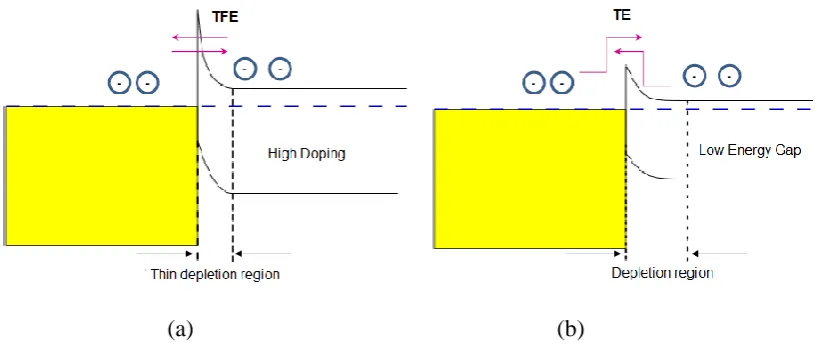
Figure 2.6 Current conduction at Ohmic contact (a) via TFE in highly doped semiconductor and (b) via TE at low Schottky barrier interface [33]... 41
Figure 2.7 Energy and diagram of Schottky contact:(a) isolated and (b) on contact [33] ... 42
Figure 2.8 Current transport by thermionic emission in: ... 43
Figure 2.9 Depletion type contacts to n-type substrates with increasing doping concentration ND: (a) Low ND, (b) Intermediate NDand (c) High ND[37] ... 44
Figure 2.10 Cross section of conventional HEMT with -doped layer ... 45
Figure 2.11 Conduction band of general depletion mode HEMT structure ... 47
Figure 2.12 Drain Current versus -doping concentration variation [41] ... 48
Figure 2.13 Electron velocity as a function of electric field for variety of Indium (In) concentrations of InGaAs [24]. ... 49
Figure 2.14 Ideal I-V characteristics of a MESFET [33] ... 52
Figure 2.15 Transconductance extracted at different Vds [44] ... 53
Figure 2.16 Frequency responses of a D-mode pHEMT under a fixed VDS and VGS 53 Figure 2.17 Id-Vg Characteristics as a function of Indium content in HEMT device [44] ... 57
Figure 2.18 ID-VGS characteristics at drain bias of 0.8V as a function of device gate length (nm). The inset presents a gm(max) at Vds=0.8V [55] ... 58
9
Figure 2.20 Submicron Epilayer Structure and Gate Design: (a) T-Shape/Mushroom
gate [18], (b) T-gate lattice-matched HEMT [14], (c) InAs channel HEMT [60],
and (d) InGaN/InN/InGaN-based double channel HEMT [34] ... 62
Figure 3.1 ATLAS Input-Output Hierarchy [80] ... 70
Figure 3.2 ATLAS Command Groups Statement [80] ... 71
Figure 3.3 Epitaxial layer profile for Sample VMBE2100 used for device structure 73
Figure 3.4 Ohmic Contact and Schottky contact defined in VMBE2100 pHEMT
model. The source and drain electrode are stretched until the end of the channel
layer. ... 75
Figure 3.5 Band profile for a HEMT as a function of sheet concentration ... 77
Figure 3.6 The electron concentration in -doped layer and carrier concentration
in Channel layer for XMBE2100 structure ... 78
Figure 3.7 Energy band diagram for the VMBE2100 pHEMT structure model in
ATLAS ... 79
Figure 3.8 Simulations of Electron Mobility in the Channel Layer (In0.7Ga0.3As
material) ... 81
Figure 3.9 Definition of the trap energy level for acceptor and donor traps in
reference to the conduction and valence band edges [80]... 87
Figure 3.10 Carrier Capturing/Releasing Mechanism in Acceptor-Like Traps [80] . 88
Figure 3.11 Modelled I-V characteristics for VMBE2100 with Trap (red line) ... 88
Figure 3.12 Trap density, NT value effects on the current-voltage characteristics .... 89 Figure 3.13 The Shift in Threshold Voltage, VT due to Trap Density, NT ... 90 Figure 4.1 Epitaxial layer structures for various in-house fabricated pHEMT samples
... 94
Figure 4.2 Schematic view of 0.25m InGaAs/InAlAs/InP pHEMT XMBE131 with
Pd/Ti/Au gate scheme as compared to the Ti/Au gate metallisation (Adapted from
[98]) ... 95
Figure 4.3 Device Mesh Structure for pHEMT structure which defined with non-cylindrical
mesh for (a) VMBE2100 and (b) XMBE131………98
Figure 4.4 Schematic device structure for VMBE2100 showing epitaxial layers
(size not to scale) ... 99
Figure 4.5 Schematic device structure for XMBE131 epitaxial layers (size not to
10
Figure 4.6 Energy band diagram (at thermal equilibrium) for VMBE2100 epitaxial
layer simulated with ATLAS Silvaco ... 100
Figure 4.7 Energy band diagram for the XMBE131 structure (at thermal
equilibrium) simulated with ATLAS Silvaco ... 101
Figure 4.8 Tonyplot visualization of Electron Concentration and Sheet Carrier
Density for (a) Single- and (b) Double Delta doping layer ... 102
Figure 4.9 (a) Sheet concentration (2DEG) and (b) Band diagram simulated at
different biasing voltage (for VMBE2100 structure) ... 103
Figure 4.10 pHEMT sample VMBE2100 (1 m gate length) characteristics
(a) Normalized current-voltage characteristics,(b) Threshold Current, VT, (c)
Normalized transconductance, gm with gm=940mS/mm at VDS=2V and (d) on-state
leakage current where VDS = 0 to 2V with 250mV steps ... 105
Figure 4.11 pHEMT sample XMBE131, 0.25m gate length (Pd gate metallisation)
(a) Normalized current-voltage characteristics with maximum drain current, (b)
Threshold Current, VT, (c) Normalized transconductance, gm with gm=940mS/mm at
VDS =2V, (d) on-state leakage current where VDS=0 to 2V with 250mV steps and (e)
Schottky Current ... 107
Figure 4.12 Typical Schottky diode forward current characteristic of InP pHEMT 108
Figure 4.13 Schottky diode forward current characteristic of XMBE131 pHEMT
modelled with different work function value. ... 110
Figure 4.14 Simulated I-V Curve (with and without) Mobility Model for
VMBE2100 ... 112
Figure 4.15 Current-Voltage Characteristics for normalised 4x200m
VMBE2100 pHEMT when only trapping mechanism activated, NT=2e17cm3 (without impact ionisation) ... 113
Figure 4.16 Modelled vs Measured I-V Characteristic for VMBE2100 ... 113
Figure 4.17 Modelled vs. Measured VT at Vds=1V for VMBE2100 pHEMT ... 114
Figure 4.18 Current-Voltage Characteristics for normalised 2x50m
XMBE131pHEMT (optimised with trap, impact model) ... 114
Figure 4.19 IDS-VGS at VDS=1V for normalised 2x50m XMBE131pHEMT
(optimised modelled vs. measured)... 116
Figure 4.20 Transconductance (meas. Vs modelled) for normalised 2x50m
11
Figure 4.21 2D Contour of Impact Ionisation rate in VMBE2100 Device Model: 118
Figure 4.22 I-V Characteristic with Impact Ionization ... 119
Figure 4.23 Kink mechanism as explained by Somerville [38] (a) Simplified device cross-section used for the model. (b) Energy bands within the extrinsic source adjacent to the gate as a function of time. (c) Drain current characteristics as a function of time. ... 120
Figure 4.24 Kink Effect Anomalies in I-V Characteristics as a Function of Trap Density: (a) Ikink is higher for high NT [111] for AlGaN/GaN HEMT and (b) Simulated I-V characteristics with NT=5x1017cm-3 ... 122
Figure 4.25 The Ikink analysis in I-V Characteristics with different trap NT value 122 Figure 4.26 Measured vs modelled cut-off frequency, fT for XMBE131 pHEMT sample ... 123
Figure 4.27 Measured vs modelled maximum frequency, fmax for XMBE131 pHEMT sample... 123
Figure 4.28 Measured vs modelled S-parameter (a) S21, S12 and (b) S11, S22 for XMBE131 pHEMT sample... 124
Figure 5.1 Physical origin of the HEMT small signal equivalent circuit model [110] ... 127
Figure 5.2 Standard form of HEMT small signal equivalent circuit [18] ... 128
Figure 5.3 Equivalent Circuit Model for FET Cold Bias Condition [18] ... 130
Figure 5.4 Method for extracting the device intrinsic Y matrix [105] ... 134
Figure 5.5 An illustration of a submicron device with a T-gate structure. ... 140
Figure 5.6 pHEMT sample XMBE131 (Ti/Au gate metallisation) (a) Normalized I-V characteristics with maximum IDS=540mA/mmat Vds=1V, (b) Threshold Voltage, VT, (c) Normalized transconductance, gm with gm=940mS/mm at Vds=2V and (d) on-state leakage current where Vds=0 to 2V with 250mV steps .... 142
Figure 5.7 Unity gain frequency, fT and maximum frequency, fmax at Vds=1V, IDS=13.19 mA for sample XMBE131 ... 143
Figure 5.8 pHEMT sample VMBE1998 (a) Normalized I-V characteristics with
maximum IDS=321 mA/mm2 (2x50m) and IDS=309 mA/mm2 (2x200m)at Vds=1V, (b) Threshold Voltage, VT at -0.89V for both device size, (c) Normalized
12
(2x200m) at Vds=2V and (d) Off-State Gate Current Leakage :Forward and Reversed ... 145
Figure 5.9 RF characteristics for pHEMT sample VMBE1998, 2x50 m and
2x200 m (a) Cut-off frequency, fT at VDS=1V, 80% gmmax and (b) Maximum
frequency, fmax extrapolated at VDS=1V, 80% gmmax ... 146 Figure 5.10 pHEMT sample XMBE56 (a) Normalized I-V characteristics with
maximum IDS=450 mA/mm2 (2x50m) and IDS=385 mA/mm2 (2x200m)at Vds=1V, (b) Threshold Voltage, VT at -0.98V (2x50m) and VT at -1.0V (2x200m) , (c)
Normalized transconductance, gm with gm=430 mS/mm (2x50m) and gm=380
mS/mm (2x200m) at Vds=1V, (d) Off-State Gate Current Leakage: forward and
reverse and (e) on-state leakage current for Vds=0 to 2V ... 148
Figure 5.11 (a) Schematic and (b) Equivalent transistor linear model [122] ... 150
Figure 5.12 Circuit Setup for Extrinsic element extraction (pinched) in ADS for
XMBE131. ... 151
Figure 5.13 Parameter extraction setup for Hot measurement ... 153
Figure 5.14 EEHEMT models for initial current-voltage parameter for DC models
... 156
Figure 5.15 Measured versus modelled XMBE131 pHEMT (a) I-V characteristics
(for VGS=0.1 V to -0.8V, -0.1V steps), (b) threshold voltage (for VDS=1V to 2V, 0.25V steps) ... 157
Figure 5.16 Curve fitting for 2x50m XMBE131 (a) Forward and Reverse Gain and
(b) Input and output reflection coefficient over frequency 40 MHz to 20 GHz
measured at 80% of maximum gm. ... 158
Figure 5.17 A Complete transistor model for XMBE131 2 x 50 m pHEMT ... 159
Figure 5.18 Summary of curve fitting for 2 x 200 μm on VMBE1998 (a) I-V curve
(b) Transconductance (c) Forward and reverse gain and (b) Reflection coefficient
against frequency ... 160
Figure 5.19 Summary of curve fitting for 2 x 200 μm on XMBE56 (a) I-V curve
(b)Transconductance (c) Forward and reverse gain and (b) Reflection coefficient
against frequency ... 161
Figure 6.1 Equivalent circuit model for NiCR resistor ... 168
13
Figure 6.3 Layout design of MMIC NiCr resistor (7.5 k) with total wire length,
L=3100 m and wire width, W=20 m. ... 169
Figure 6.4 An example for coplanar interdigital capacitor for MMICs [139] ... 170
Figure 6.5 Equivalent circuit for MMIC Capacitance ... 171
Figure 6.6 Modelled circuit for MIM Capacitor setup in ADS... 172
Figure 6.7 S-parameter results for an 8pF MIM capacitor over the frequency ... 173
Figure 6.8 Equivalent circuit for spiral inductor ... 174
Figure 6.9 Schematic of equivalent circuit for spiral Inductor modelled in ADS. .. 175
Figure 6.10 S-parameter for 14 nH Spiral inductor over wide range frequency... 176
Figure 6.11 Layout design for 14 nH Spiral inductor ... 176
Figure 6.12 Power reflection coefficients for a 2-port microwave network [110] .. 177
Figure 6.13 Reflection coefficients for a general microwave 2-port network ... 180
Figure 6.14 Schematic diagrams of basic LNA topologies [43] ... 184
Figure 6.15 Inductive Peaking Schematic [142] ... 184
Figure 6.16 Graph of typical I-V characteristic and operating bias point for HEMT ... 185
Figure 6.17 Circuit diagram of pHEMT with biasing circuit with inductor ... 186
Figure 6.18 General Input and output circuit of 2-port network ... 187
Figure 6.19 Single Stage circuit for 4-8 GHz frequency range... 189
Figure 6.20 Gain, Noise figure, Stability and Input and output reflection results ... 190
Figure 6.21 Double Stage LNA circuit for 4-8 GHz frequency range ... 191
Figure 6.22 The gain, input and output reflection results for C-band Double-stage LNA ... 192
Figure 6.23 Single Stage circuit for 8-12 GHz frequency range... 194
Figure 6.24 Gain, Noise figure and Input/output reflection results for SSLNA at 8-12 GHz frequency range ... 194
Figure 6.25 Double Double Stage LNA (DSLNA) circuit for 8-12 GHz frequency range ... 195
Figure 6.26 Maximum Gain, Noise Figure, Stability factor, and input and output reflection results for DSLNA operating at 8-12 GHz ... 196
Figure 7.1 Schematic of RTD Structure [153] ... 199
14
Figure 7.3 Generic I-V characteristic of an RTD, showing peak... 202
Figure 7.4 Generic epilayer structure of RTD using In0.8Ga0.2As/AlAs material
system studied in this project. ... 204
Figure 7.5 Band diagram and doping profile for XMBE277 RTD (size 3m 3m)
... 205
Figure 7.6 IV Characteristics for various samples RTD with different barrier
thicknesses ... 206
Figure 7.7 IV Characteristics for various samples RTD with different spacer
thicknesses ... 208
Figure 7.8 Modelled and measured current density for sample XMBE277 (a) on
large area mesa (3µmx3µm) and (b) on sub-micrometer area mesa (2µmx0.35µm)
... 211
Figure 7.9 Electron particle-wave duality (quantum tunnelling)[143] ... 213
Figure 7.10 A Symmetrical double barrier regions in RTD ... 213
Figure 7.11 I-V Characteristics (XMBE277 RTD) with various spacer thicknesses
... 216
Figure 7.12 Modelled and measured IV for XMBE301 RTD with doping variations
... 217
Figure 7.13 Modelled and measured IV for XMBE301 RTD with doping variations
... 217
Figure 7.14 I-V Characteristics (XMBE302 RTD) with various barrier thicknesses
... 219
Figure 7.15 I-V Characteristics (XMBE308 RTD) with various barrier thicknesses
... 219
Figure 7.16 Optimised model for XMBE308 with barrier thickness modification 220
Figure 7.17 Modelled IV Characteristics for XMBE301 RTD with tQW variations ... 221
15
LIST OF TABLES
Table 2.1 Lattice constant and energy band gap of common III-V binary and
ternary compound semiconductors at 300 K [26, 27] ... 33
Table 3.1 VMBE2100 Electrodes definition in ATLAS ... 74
Table 3.2 Parameters to specify a doping profile [80] ... 76
Table 3.3 Generation/Recombination Mechanism Models ... 83
Table 4.1 Hall measurement data at 300 K (room temperature) and 77 K for VMBE2100 and XMBE131 pHEMT device ... 96
Table 4.2 Ideality factor (n) measurement data vs modelled with various metal work function ... 110
Table 4.3 Impact Ionization Parameters Applied for the Modelling [45] ... 117
Table 5.1 Epitaxial structure for various pHEMT samples fabricated at the University of Manchester ... 138
Table 5.2 Hall measurement data at 300 K (room temperature) and 77 K for VMBE1998, XMBE56 and XMBE131 pHEMT device ... 139
Table 5.3 Biasing for in-house fabricated pHEMT sample devices (a VDS=1V) .... 141
Table 5.4 Ideality factor and Barrier height for VMBE1998 pHEMT sample ... 145
Table 5.5 Ideality factor and Barrier height for XMBE56 pHEMT sample ... 149
Table 5.6 Transconductance and RF characteristics XMBE56 pHEMT sample ... 149
Table 5.7 Table of Extrinsic values for various pHEMT sample devices (VDS=1V,80% gmmax or ~ 10% Idss) ... 152
Table 5.8 Table of intrinsic parameters for all devices at VDS=1V, 10% IDSS ... 154
16
Table 6.1 Parameter value used for in-house fabricated spiral inductor ... 175
Table 6.2 Specification for SSLNA and DSLNA in C-band frequency ... 188
Table 6.3 Component values used in C-band DSLNA design ... 191
Table 6.4 Target Specification for X-band LNA compared to related works ... 193
Table 7.1 RTD Epitaxial Structure (XMBE277, tb=13 Å, 1ML ~ 2.7 Å [143]) ... 205
Table 7.2 Peak current density and PVCR for various RTD sample [142] ... 206
Table 7.3 RTD Epitaxial Structure (XMBE308, tS=25Å, 1 ML ~2.9 Å [143]) ... 207
Table 7.4 Figure of merits for various RTD samples... 208
Table 7. 5 Fitting parameters for large area and submicron RTD on sample XMBE277 ... 212
17
LIST OF ABBREVIATIONS
2DEG Two-Dimensional Electron Gas
ADS Advanced Design System
ASKAP Australian SKA Pathfinder
ATA Allen Telescope Array
CAD Computer Aided Design
CMOS Complementary Metal Oxide Semiconductor
CPW Coplanar Waveguide
DC Direct Current
HBT Heterojunction Bipolar Transistor
HEMT High Electron Mobility
ICCAP Integrated Circuit Characterization and Analysis Program
IF Intermediate Frequency
LNA Low Noise Amplifier
MBE Molecular Beam Epitaxy
MESFET Metal Semiconductor Field Effect Transistor
MMIC Monolithic Microwave Integrated Circuit
MOCVD Metal-oxideChemical Vapour Deposition
MODFET Modulation Doped FET
M&N Microelectronic and Nanostuctures NF Noise Figure
NFmin Minimum Noise Figure
pHEMT Pseudomorphic High Electron Mobility Transistor
PNA General-purpose Network Analyser
QW Quantum Well
RF Radio Frequency
18
SDHT Selectively Doped Heterostructure Transistors
SKA Square Kilometre Array
TEGFET Two Dimensional Electron Gas Field Effect Transistors
Notations
Cds,gs Drain/gate to source capacitance
Cgd Drain to gate capacitance
Cpg,pd,ps Pad capacitances to electrodes
∆Ec Conduction band discontinuity
∆Eg Band gap difference of heterojunction materials
∆Ec Valence band discontinuity
Eg Band gap energy
Ebr Breakdown voltage
Efn Electron Quasi fermi level
EF Fermi Level
Lg,s,d Gate/Source/Drain contact inductance
NC Effective density of states
P Polarization
Psp Spontaneous polarization
Ppz Piezo-electric polarization
q Electron charge
Rg,s,d Gate/Source/Drain contact resistance
Rds,gs Drain/gate to source resistance
vsat Saturation velocity
VT Threshold voltage of HEMT
xAlGaN Aluminium molefraction in GaN
19
ABSTRACT
The University of Manchester
Candidate: Warsuzarina binti Mat Jubadi Degree: Doctor of Philosophy (PhD)
Thesis Title: Modelling of Advanced Submicron Gate InGaAs/InAlAs pHEMTs and RTD Devices for Very High Frequency Circuits
Date: May 2015
InP based InAlAs/InGaAs pseudomorphic High Electron Mobility Transistors (pHEMTs) have shown outstanding performances, which makes them prominent in high frequency mm-wave and submillimeter-wave applications. However, conventional InGaAs/InAlAs pHEMTs have major drawbacks, i.e., very low breakdown voltage and high gate leakage current. These disadvantages degrade device performance, especially in Monolithic Microwave Integrated Circuit (MMIC) low noise amplifiers (LNAs). The optimisation of InAlAs/InGaAs epilayer structures through advanced bandgap engineering together with gate length reduction from 1 m into deep sub-μm regime is the key solution to enabled high breakdown and ultra-high speed, low noise pHEMT devices to be fabricated. Concurrently, device modelling plays a vital role in the design and analysis of pHEMT device and circuit performance. Physical modeling becomes essential to fully characterise and understand the underlying physical phenomenon of the device, while empirical modelling is significant in circuit design and predicts device’s characteristic performance.
In this research, the main objectives to accurately model the DC and RF characteristics of the two-dimensional (2D) physical modelling for sub-μm gate length for strained channel InAlAs/InGaAs/InP pHEMT has been accomplished and developed in ATLAS Silvaco. All modelled devices were optimised and validated by experimental devices which were fabricated at the University of Manchester; the sub-micrometer devices were developed with T-gate using I-line optical lithography. The underlying device physics insight are gained, i.e, the effects of changes to the device’s physical structure, theoretical concepts and its general operation, hence a reliable pHEMT model is obtained. The kink anomalies in I-V characteristics was reproduced and the 2D simulation results demonstrate an outstanding agreement with measured DC and RF characteristics.
The aims to develop linear and nonlinear models for sub-μm transistors and their
implementation in MMIC LNA design is achieved with the 0.25 m
In0.7Ga0.3As/In0.52Al0.48As/InP pHEMT. An accurate technique for the extraction of empirical
models for the fabricated active devices has been developed and optimised using Advance Design System (ADS) software which demonstrate excellent agreement between experimental and modelled DC and RF data. A precise models for MMIC passive devices have also been obtained and incorporated in the proposed design for a single and double stage MMIC LNAs in C- and X-band frequency. The single stage LNA is designed to achieve maximum gain ranging from 9 to 13 dB over the band of operation while the gain is increased between 20 dB and 26 dB for the double stage LNA designs. A noise figure of less than 1.2 dB and 2 dB is expected respectively, for the C- and X-band LNA designed while retaining stability across the entire frequency bands.
Although the RF performance of pHEMT is being vigorously pushed towards terahertz region, novel devices such as Resonant Tunnelling Diode (RTD) are needed to support future ultra-high speed, high frequency applications especially when it comes to THz frequencies. Hence, the study of physical modelling is extended to quantum modelling of an advanced In0.8Ga0.2As/AlAs RTD device to effectively model both large size and
25
1 CHAPTER 1
INTRODUCTION
1.1 Overview
The High Electron Mobility Transistor (HEMT) and Pseudomorphic High Electron
Mobility Transistor (pHEMT) are Field Effect Transistors (FET). HEMTs operate in
a similar manner to MESFET but extend the performance of FET by taking
advantage of the large band discontinuities in the band structures of the constituent
semiconductor materials. Basically, HEMTs structure consists of compositional
compound materials that are lattice-matched to the substrate. However in the
pHEMT structure, the channel material is so thin that the crystal lattice stretches
“pseudomorphically” to occupy the spacing of the nearby material. Consequently, it
allows better performance due to the larger bandgap difference compared to the
lattice-matched structure. The formation of quantum well and the two dimensional
electron Gas (2DEG) in the channel provides HEMT with a high electron mobility
and high carrier density, leading to low noise figures and higher cut-off frequency
[1].
Amongst all material systems in the III-V compound semiconductors, the
InGaAs/InAlAs material system has the most desirable band structure and transport
properties (carrier mobility, saturation velocity, etc). This material system offers
pHEMT devices with high electron sheet charge density and excellent carrier
confinement in the channel, resulting in superior electron transport translating into
higher transconductance (gm), current gain cutoff frequency (fT) and lower noise figure (NF). Hence, the InGaAs/InAlAs has become an advanced material system
for high-speed, high-frequency and even in the lower frequency range of 0.9 GHz
and 1.9 GHz that are used for mobile communication [2]. Current development of
InP based InAlAs/InGaAs HEMTs have demonstrated excellent high frequency and
26
dominate the microwave and millimetre wave applications and low noise amplifiers
(LNAs) fields [6, 7, 8].
The superior performance of InP based InAlAs/InGaAs pHEMTs as compared to the
GaAs-based HEMT [9] makes them the most preferred candidates for the active
devices selection and also an important aspects in the fabrication of Monolithic
Millimeter Wave Integrated Circuit (MMIC) LNAs. The design of MMIC LNAs
itself has emerged from the design for very low frequency, low noise figure, very
high power, etc. For over a decade, the advancement in millimeter wave
semiconductor technologies has been strongly driven by military requests such as
sensor/radar application [10]. There are also an increasing number of wireless civil
applications, i.e telecommunication-, sensors- and navigation-systems that are ever
demanding for more and more low-noise and power devices at high frequencies.
Undoubtedly, these systems could be realised with the outstanding combination of
high frequency operation and low noise performance of the InGaAs/InAlAs/InP
pHEMT devices.
1.2 Project Motivation and Objective
Recent advances in Metal Organic Chemical Vapour Deposition (MOCVD) and
Molecular Beam Epitaxy (MBE) epitaxial growth techniques for III-V compound
semiconductor systems have made it possible to grow extremely high-quality III-V
heterojunction structures. Current development of InAlAs/InGaAs HEMTs have
demonstrated excellent high cutoff frequency of 625 GHz up to 1 THz and high-gain
performance [3, 4] and dominate the millimeter wave applications, i.e., low cost
LNA [3] and Ka-band MMIC LNAs [6]. The previous work conducted by the
Manchester group on novel pHEMT devices [11,12] and hence the MMIC LNA
development for the SKA was initiated at the SKA-low frequency (L-band) [13, 14]
using a one micron gate length device.
With the device size scaled down to the nanometer regime and various epitaxial
layer structures being designed and optimized, physical modeling becomes essential
27
devices. Semiconductor modelling based on physical models [15, 16] can prove to be
very helpful in the development of such transistors. The empirical modelling [17,18]
is also required to accurately model and estimate the performance analysis the linear
and nonlinear behaviour of the designed circuits , i.e. LNA over a range of frequency
and characterize the device technological process. The development and verification
of device simulation tools have become desirable as to compare statistically analysed
measured data. With the aid of modelling, the time and cost of device fabrication and
characterization undoubtedly can be considerably reduced [19]. This research aims
to employ the advances of modelling tools, SILVACO simulation package and
Advanced Design System (ADS) to appreciate the underlying device physics of the
device towards the device output characteristics, to reproduce both the DC and RF
device characteristic, and investigate the correlation of the device physics to the
output characteristics. The initial work of the device modelling of 1 m gate device
will be extended to the deep submicrometer gate regime and aim to develop models
for new transistors and their implementation in the design and fabrication of
advanced integrated circuits using the extensive facilities available at the University
of Manchester.
Despite of the high cut-off frequency achievements reported for InP pHEMT in the
terahertz region, i.e. [20] and [21], novel devices are needed which are able to
support future ultra-high speed, high frequency applications; especially when it
comes to sub-THz or THz frequencies (operating at room temperature). The
Resonant Tunnelling Diode (RTD) might well be the solution to this problem with
its ability to provide a very high fundamental frequency well into the THz region.
Therefore, the study of physical modelling is extended to quantum modelling for an
advanced InGaAs/AlAs RTD device. The purpose of this extended work is to
effectively model the RTD using Silvaco’s ATLAS software; particularly with
respect to the peak current density, peak-to-valley-current ratio (PVCR), and
28
1.3 Scope of thesis
This thesis presents the physical and empirical modelling of advanced
InGaAs/InAlAs pHEMT for the development of low noise amplifier (LNA) designs
to fulfil the requirements of the (8.0 to 12 GHz) band of the Square Kilometre Array
(SKA) [22]. During the preliminary work, the transistor used in this project
employed a 1μm gate length with multiple sized gate widths. The modelling and
circuit designs are then progressed with the submicrometer gate InGaAs/InAlAs
pHEMT to facilitate higher frequency applications. The transistors were in-house
fabricated at the University of Manchester and the measurement of the transistors is
carried out at room temperature. The proposed design is a Monolithic Microwave
Integrated Circuit (MMIC) that combine high performance with low cost and avoids
expensive and labor intensive external components (especially discrete inductors
used for the input of the LNA). In this work, the advances in the InGaAs/InAlAs
material system is fully utilised in the submicron gate length pHEMT and the study
is extended into a simpler one dimensional structure of a two terminal device, the
InGaAs/AlAs resonant tunnelling diode (RTD).
1.4 Thesis Outline
The organization of the remainder of this thesis is as follows:
Chapter 2 provides insights into the fundamental theory of semiconductor device physics for heterojunctions and HEMTs structure background. This chapter deals
with the literature review of the basic concepts of III-V compound semiconductors.
The development of different III-V FET devices in relation to the advancement of
material engineering and their contribution to RF applications are presented. A
comparison between the different FET structures (MESFET, HEMT and pHEMT)
and material systems (InGaAs-AlGaAs, InGaAs-InAlAs) and the advantage of
InP-based pHEMT for low noise and high speed applications is outlined. The discussion
continues with an extensive study of the physics and operation of the devices. At the
end of the chapter, some important physical parameter extraction methods are
29
Chapter 3 highlights the significance of device simulations, introduces the simulation tools used in the development of the physical modelling performed in this
work. Detail procedures of the device modelling of pHEMTs structure are presented,
i.e. meshing, structure and parameter definitions, and physical models, and
numerical methods. A detail explanation of the concepts of device modelling and
current-transport equations used in this project is presented.
Chapter 4 briefly explains the fundamental models that are used in the simulation work for the small signal model. In this chapter a physically based model for various
samples of the in-house fabricated pHEMTs has been developed, providing an
insight to the internal device behaviour. The DC and RF characteristics of the two
dimensional physical device simulations are compared with the experimental results
which were fitted and analysed. The modelled device simulation shows excellent
agreement with the experimental results.
Chapter 5 explains the empirical model parameters and device modelling steps for the pHEMT device. The empirical models for three different epitaxial layers with
various device sizes and gate length are presented. The agreements between the
modelled and measured parameter are discussed and analysed. An optimized
pHEMT model which is used in the LNA design and a brief study on the device’s
noise characteristics are presented at the end of this chapter. The results from device
empirical modelling provides a guide for active device selection for LNA circuit
designs.
Chapter 6 begins with the background of Monolithic Microwave Integrated Circuit (MMIC) and its advantages in the integrated circuit roadmap. This is followed by an
outline of the LNA theoretical concept which is used to examine the requirements of
a complete system design. The target specifications of the MMIC LNA design are
then addressed; the performance constraints and compromises that arise in the design
of circuit topologies, biasing networks and matching configurations are also
discussed. The design and analysis of the single input single-ended output, single
and double stage LNAs are presented using all of the criteria discussed in Chapters
30
of this chapter, the target specifications attained from the simulation of the single-
and double-stage MMIC LNA for C-band and X-band frequency range are presented
and discussed. The layout designs of these LNA circuits are also developed and
presented.
Chapter 7 demonstrates a one-dimensional physical modelling for various sample of large-siz and submicrometer In0.8Ga0.2As/GaAs Resonant Tunneling Diode (RTD) device. The concept, operation principle and the applications of RTD in Terahertz
(THz) region are explained at the beginning of the chapter. The modelling of the two
terminal RTD device focuses on the DC analysis, which is mainly to reproduce the
I-V characteristics of experimental devices, namely the negative differential resistance
(NDR), NDR peak voltage, VP (voltage at peak current) and the peak current
density(IP). The model optimisation based of the device structure, i.e. spacer layer,
barrier layer and quantum well layer thicknesses are also studied. The modelled
device simulation for DC analysis shows excellent agreement with the experimental
results.
Finally, Chapter 8 summarises the work that has been discussed in the earlier chapters and suggests some potential future research to further extend the work
31
2 CHAPTER 2
THEORY AND BACKGROUND OF PSEUDOMORPHIC HIGH
ELECTRON MOBILITY TRANSISTOR
2.1 Introduction
For the past decades, the power of electronics has been driven by an increase in the
density of silicon complementary metal–oxide–semiconductor (CMOS) transistors
and the progression to their logic performance. The semiconductor chips are
becoming more powerful, smaller and more economical and energy efficient.
However, as the scaling of silicon transistor is now reaching its limits, the III-V
compound semiconductors are now becoming the key choice to continue the
microelectronic revolution for high speed and high frequency devices. The
outstanding electron transport properties and frequency response of these materials
might be central to the development of nanometre-scale logic transistors [23]. For
example, the electron mobility in InGaAs and InAs HEMT is more than 10 times
higher than in silicon at a comparable sheet density. In the early development,
HEMTs, also known as Modulation Doped Field Effect Transistors (MODFETs),
Two-dimensional Electron Gas Field Effect Transistors (TEGFETs), Heterojunction
Field Effect Transistors (HFETs) or Selectively Doped Heterostructure Transistors
(SDHTs) was originally developed for high speed applications and these devices
were discovered to exhibit a very low noise figure. This is related to the nature of the
two-dimensional electron gas (2DEG) and the fact that there are less electron
collisions in the channel [6].
The basic fundamental which govern the development of HEMTs are explained in
this chapter. An introduction to heterojunction, their band structures, formation of
quantum wells, carrier confinement and 2DEG will be discussed. The HEMT and
pHEMT structures and their operational principles are summarized. Some of the
applications of pHEMTs and works concentrating in the pHEMTs design in the
32
2.2 Hetero Junction Structure
Generally, HEMT structures are based on epitaxially grown layers with different
compositions and energy band gaps. When these different semiconductor layers are
brought together, they form heterojunctions. The principle parameters for
heterostructures are the difference of energy bandgaps (Eg) and the lattice constant
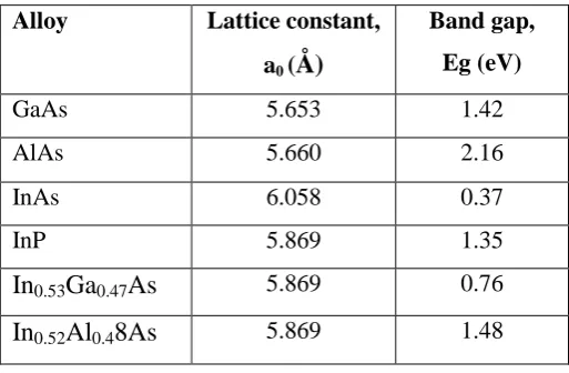
(a) for the two semiconductor materials. Figure 2.1illustrates the lattice constant and
energy gap parameters for various III-V material system that are of interest to the
work presented here. These parameters play a very important role in the advanced
[image:27.595.122.515.292.555.2]bandgap engineering to optimize device characteristics.
Figure 2.1 The energy gap of III–V compounds and ternary derivatives
as a function of lattice constant [24]
The ternary compound semiconductor materials that are lattice matched to GaAs and
InP substrates are shown. For example, the AlAs, AlxGa(1-x)As, (for all values of x)
and In0.48Ga0.52P is lattice match with GaAs. Consequently, the InxGa(1-x)As and
InxAl(1-x)As are lattice matched to InP only at a single fixed mole fraction (x ~0.52).
Practically, the materials chosen must have a very close lattice constant to minimise
the disturbance at the heterointerface. However, for various materials that have
33
semiconductor materials to match the size of the crystal lattices. Therefore, the
resulting lattice constant and the energy band gap can be approximated using
Vegard’s law [21, 22] as in Equation 2.1, where x is the mole fraction and AZ and BZ
are the binary compound lattice constant and band gap values,
𝑎𝑎𝑙𝑙𝑜𝑦= 𝑥AZ + (1 − 𝑥)BZ Equation 2.1
The lattice constant and band-gap energy for various GaAs and InP-based materials
are given in Table 2.1 [26,27]. Enhancements in epitaxial growth techniques have
enabled the possibility of growing lattice mismatched heterostructures [27]. In this
situation, the lattice atoms change abruptly between the two semiconductor materials
with dissimilar energy band gaps and lattice constants [24, 25]. This growth
[image:28.595.190.447.396.564.2]technique is known as pseudomorphism and will be discussed in the next section.
Table 2.1 Lattice constant and energy band gap of common III-V binary and
ternary compound semiconductors at 300 K [26, 27]
Alloy Lattice constant,
a0 (Å)
Band gap,
Eg (eV)
GaAs 5.653 1.42
AlAs 5.660 2.16
InAs 6.058 0.37
InP 5.869 1.35
In0.53Ga0.47As 5.869 0.76
In0.52Al0.48As 5.869 1.48
For an InP substrate, the lattice matched In0.52Al0.48As is usually used as a buffer as it has a large band gap, resulting in improved insulation; and In0.53Ga0.47As as a channel (due to its high mobility) followed by In0.52Al0.48As as a barrier (large Ec).
Over the years, the state-of-art compound semiconductor technology has moved
from GaAs channel (lattice constant =5.64Å) to InxGa1-xAs/InP channels (5.87Å)
34
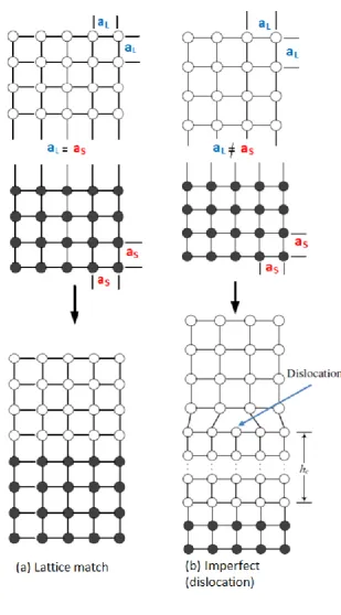
2.2.1 Lattice Matched and Pseudomorphic Material System
Ideally, heterostructures are formed by semiconductors with the same crystal
structures and the same lattice constant. A HEMT structures grown with the same
lattice constant are referred to as lattice matched HEMTs, i.e. In0.53Ga0.47As and In0.52Al0.48As (lattice matched to InP). Structures with slightly different lattice constant are known as Pseudomorphic HEMTs (pHEMTs). In modern epitaxial
growth techniques, the thickness of lattice mismatched layers is kept within a certain
critical thickness limit and the deposited layer must be very thin to avoid defect or
dislocation formation [23, 29]. This new layer is called “pseudormorphic” as it alters
its original crystal structure and physical properties, i.e., InGaAs-InAlAs,
AlGaAs/InGaAs. For lattice mismatched, the atoms at the hetero-interface have to
slightly adjust their positions in order for them to conserve the geometry of the
lattice. The adjustments of the atomic position will result in a small strain at the
interface. The critical thickness of grown epilayer (hC) and the strain () is given by
Equation 2.22 and Equation 2.3. Respectively, aS and aL denotes the lattice constant
for substrate and grown epilayer.
ℎ𝐶 =
𝑎𝑆
2𝜀 Equation 2.2
𝜀 =𝑎𝐿−𝑎𝑆
𝑎𝑆
Equation 2.3
The Figure 2.2 illustrates the crystal formation of the binary and ternary compound
semiconductor material. In Figure 2.2 (a), aL is in lattice matched with aS, and hence
the over-layer and base material atoms at the crystal interface are not required to
adjust their positions relative to each other. However, lattice mismatched in the
semiconductor may result in defects due to dislocations, as shown in Figure 2.2 (b).
Above the critical thickness, the excessive strain energy is released by the formation
of dislocations where some of the bonds are missing or extra bonds appear. These
dislocations adversely affect the electrical characteristics of a device by creating
localized states which act as traps for the charge carriers [29]. Materials that are not
in lattice matched or have different inter-atomic lattice spacing are known as
35
structure under compressive and tensile strains are shown in Figure 2.2 (c) and
Figure 2.2 (d) respectively. When aL is larger than aS, the resultant relaxed material
[image:30.595.159.469.164.723.2]36
Figure 2.2 Conceptual formation of (a) lattice matched, (b) lattice mismatched
37
2.2.2 Band Discontinuity
Energy band discontinuity is the most important aspect of heterojunctions. It is an
interesting features i.e., in HEMTs which can be used to modify the transport of
charge carriers. The junction of two semiconductors with a difference in energy
bandgaps results in an abrupt change in the energy band diagram of the
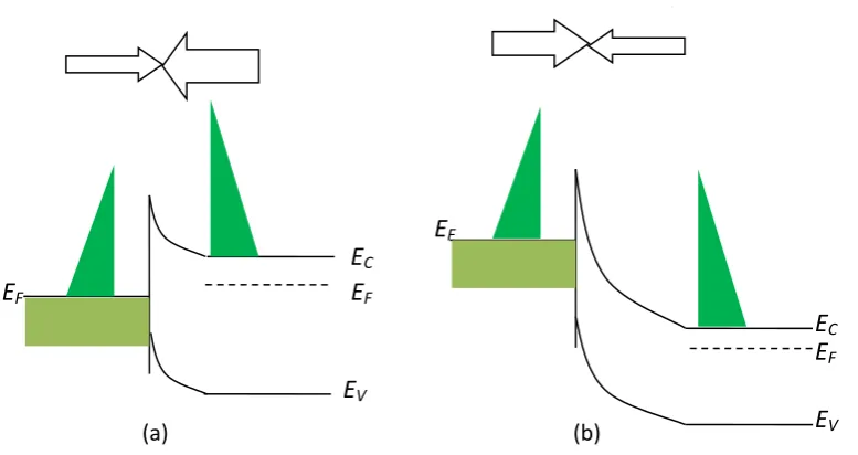
heterostructure. Figure 2.3 shows the energy band diagram of two isolated
semiconductors with the notation given by: EC and EV indicating conduction and valence bands, Eg1 and Eg2 the energy band gap for material A and material B, χ is
the electron affinities, EF is the Fermi level, Ec the electron affinity, and Ec and Evrepresenting the conduction and valence band discontinuities between the two
materials [33].
[image:32.595.112.506.330.543.2](a) (b)
Figure 2.3 Energy Band Diagrams for wide and narrow bandgap semiconductor
(a) before and (b) after contact
The energy-band model of an ideal, abrupt heterojunction, was first established by
Anderson [34]. The model assumes that Ec was equal to the difference in electron
affinities, as shown in Equation 2.4 and Equation 2.5.
𝐸𝑐=χ1− χ2 Equation 2.4
38
Similarly, this could be written using Equation 2.6 and Equation 2.7,
𝐸𝑔 =𝐸𝑔1 −𝐸𝑔2 Equation 2.6
𝐸𝑔 =𝐸𝑐 +𝐸𝑣 Equation 2.7
In most semiconductors, the band gap engineering is very effective to attain
numerous amounts of junction discontinuities. A larger band discontinuity, EC will
lead to better carrier confinement and therefore a higher carrier concentration at the
2-DEG interface. The InAlAs/InGaAs/InP material system has many significant
advantages over the AlGaAs/GaAs [24] or AlGaAs/InGaAs/GaAs material systems.
The EC between In0.52Al0.48As/In0.53Ga0.47As layer in InAlAs/InGaAs/InP material
system (> 0.5eV) is higher than the EC between Al0.2Ga0.8As/In0.15Ga0.85As layer (~
0.3 eV) in the pseudomorphic AlGaAs/InGaAs/GaAs material system. The band
discontinuity is even lower for Al0.30Ga0.70As/GaAs hereterojunction where the EC is only 0.24 eV [16]. This property, therefore makes In0.52Al0.48As/In0.53Ga0.47As/InP
a prominent and suitable candidate for high-speed devices application with greater
flexibility over carrier control at the junction.
2.2.3 Quantum Well and 2-DEG
When a thin layer of (~ 100 Å) of low band gap semiconductor material (e.g. GaAs)
is sandwiched between two similar high band gap semiconductors (e.g. AlGaAs), a
Quantum Well (QW) can be formed in the heterostructure. Such a heterojunction
boundary will experience discontinuities at the edges of the conduction band and
valence band with a QW generated for the carriers (electrons and holes) as illustrated
in Figure 2.4. The dopants in the high band gap layers can supply the carriers to the
quantum well. When the bottom of the quantum well is below the Fermi level, the
high energy donors will go down to the well, hence creating a Two Dimensional
Electron Gas (2DEG). This is shown in Figure 2.4 (c). The electron is free to move
parallel to the interface, and so is quasi two-dimensional. However, the electrons in
39
i.e. the crystal growth direction [35]. Careful choice of the materials and alloy
[image:34.595.190.467.139.461.2]compositions allow control of the carrier densities within the 2DEG.
Figure 2.4 An ideal undoped square shape quantum well (a) Structure, Energy band
diagram, and (c) Conduction band diagram if AlGaAs is n-doped [35]
2.3 Metal Semiconductor Contacts
Metal-semiconductor contacts are present in every semiconductor device. There are
two types of contact for a metal-semiconductor junction; Schottky contact or ohmic
contact depending on the nature of the interface. The details of these contacts are
40
2.3.1 Ohmic Contact
An ohmic contact is formed if no potential barrier exists between the metal and
semiconductor. It is a non-rectifying contact and does not control the flow of current,
thus the current flows equally in both directions (reverse and forward) with linear
I-V characteristic. On top of that, an ohmic contact should have an insignificant
contact resistance, RC relative to the series resistance, rs of the semiconductor so that
zero or very small current loss occurs across the device. There are 2 types of ohmic
contact: (1) for n-type semiconductor; the metal workfunction, Фm must be closer to
or smaller than the semiconductor electron affinity χ. Therefore, Фm must be smaller
than the work-function of semiconductor Фs, i.e. Фs > Фm, as shown in Figure 2.5
(2) for a p-type semiconductor, Фm must be close to or larger than the sum of
electron affinity and energy bandgap of the semiconductor, which is usually
impractical. Hence p-type ohmic contacts are a lot more difficult to fabricate than
[image:35.595.119.510.394.612.2]n-type ones.
Figure 2.5 Band diagram of a metal-semiconductor interface:
(a) before contact and (b) after contact [33]
Practically, there are two ways in achieving a good ohmic contact in semiconductor
processing: either by high semiconductor doping layer or through a low Schottky
barrier height at metal-semiconductor junction. At any metal-semiconductor contact,
there always exists a Schottky barrier [33]. The carriers must overcome this barrier
Vacuum Level
EV
EF
EC
EFm
Semiconductor qФs
qm
EV
EF
qχ
Metal Metal Semiconductor
Eg
EC
qФs
qФm
Vacuum Level
qχ
41
in order to travel between the metal and semiconductor sides. When the
semiconductor is heavily doped, i.e. ND 1019 cm-3, the depletion width and consequently the barrier width near the metal-semiconductor contact will be reduced.
Electrons now can overcome this barrier and tunnel through it as the depletion width
becomes sufficiently narrow. This mechanism is known as Thermionic Field
Emission (TFE) [36]. Alternatively, the barrier height is reduced by means of a low
energy gap material at the semiconductor side. Here, the electrons have energies
larger than the potential barrier and Thermionic Emission (TE) takes place by
electrons moving over the barrier [33]. Figure 2.6 illustrates the TFE and TE
mechanism at the Schottky barrier interface.
[image:36.595.116.524.300.472.2](a) (b)
Figure 2.6 Current conduction at Ohmic contact (a) via TFE in highly doped semiconductor
and (b) via TE at low Schottky barrier interface [33]
2.3.2 Schottky Contact
A Schottky contact (also known as rectifying contact), permits the flow of current in
one direction and provides a barrier to the flow of current in the opposite direction.
In Schottky contact, the semiconductor function, Фm is smaller than the
work-function of the metal, Фm (Фs < Фm). Figure 2.7 (a) illustrates a metal to
semiconductor interface before and after forming the Schottky contact for n-type
semiconductor and metal contact. On contact, electrons from the semiconductor
conduction band flow into lower energy states of metal, till a constant Fermi level is
achieved at equilibrium condition. The flow of electrons will then leave a positive
charge of ionised donor in the semiconductor which creates the depletion region of
42
results in a potential barrier, Фb, at the interface and a built-in potential, Vbi that restricts further diffusion of electrons from semiconductor to metal. The exact shape
of the conduction and valence bands is determined by solving the Schrödinger and
[image:37.595.135.530.179.394.2]Poisson equations self-consistently.
Figure 2.7 Energy and diagram of Schottky contact:(a) isolated and (b) on contact [33]
The built-in potential is given by Equation 2.8:
Vbi = Фb - Фn Equation 2.8
where Фn is the potential difference between the minimum of conduction band (EC)
and Fermi level EF, i.e.
n = 𝐸𝐶−𝐸𝑞 𝐹 Equation 2.9
The potential barrier, Фb, formed at the interface is related to the metal work-function, Фm and semiconductor electron affinity,s as in Equation 2.10 and Equation 2.11:
B = m -s Equation 2.10
S =S - n Equation 2.11
Vacuum Level EV EF EC EF qФb qVbi Semiconductor qФs
qm
EV
EF
qχ
Metal Metal Semiconductor
Eg
EC qФs
qФm Vacuum Level qχ Eg Xdep - - - - - - + + - + + - qVn
43
Under zero bias condition, the net current flow between semiconductor to metal is
zero because the same amount of current flows from semiconductor to metal and
vice versa. However, under forward and reverse bias conditions, the flow of current
[image:38.595.126.515.214.420.2]transport changes due the changes in the Vbi. These conditions are illustrated in Figure 2.8 in which B remains constant [12] in both figures.
Figure 2.8 Current transport by thermionic emission in:
(a) forward bias and (b) reverse bias [33]
When a positive bias, e.g., VF is applied to a metal, it will experience forward bias
condition. Under this condition, the Fermi level, EF will be shifted up and the built-in
voltahe, Vbi will be reduced by a voltage VF as illustrated in Figure 2.8 (a). The
Figure 2.8 (b) shows that if a negative bias, i.e, -VR is applied to the metal, a reverse
bias condition is achieved. In reversed bias condition, the Fermi level will be shifted
down and the built-in-potential will increase by a voltage VR. In a pHEMT, the
quantity of electrons flow from metal to semiconductor under reverse bias condition
is also known as leakage current [31]. The leakage current is one of the unwanted
drawback for a pHEMT device which degrades its performance, particularly at high
frequency applications.
EC
EV
EF EF
(a) EV
EF
EC
EF
44
[image:39.595.91.533.69.311.2](a) (b) (c)
Figure 2.9 Depletion type contacts to n-type substrates with increasing doping concentration
ND: (a) Low ND, (b) Intermediate NDand (c) High ND[37]
The mechanism of TE, TFE and FE at the barrier is shown in Figure 2.9.
Theoretically, a metal with a higher Фm will yield a larger Schottky barrier on the
same semiconductor. But this is not quite valid in practice. There is always an
intermediate layer, contributing to the surface contamination of the metal or the
surface states of the semiconductors such as native oxides or dangling bonds after
etching, formed in between the metal and semiconductor. As a result, the Fermi level
of a semiconductor will pin at the surface [38] of the intermediate layer before
equilibrium is achieved. The resulting barrier height is not sensitive to the change of
metal work function and such phenomenon is called Fermi-level pinning [33]. Thermionic Emission (TE):
Carriers are thermally excited over the barrier
(Low ND)
Thermionic Field Emission (TFE): Carriers are thermally excited to an energy where the barrier is sufficiently narrow for the
tunneling to take place (Intermediate ND)
Field Emission (FE): Carriers can tunnel through
45
2.4 Introduction to High Electron Mobility Transistors (HEMTs)
HEMTs are very similar to Metal Semiconductor Field Effect Transistors (MESFET)
in terms of structure and operations, but the key difference is the heterojunction
structures. By bringing two dissimilar semiconductors to the junction, a potential
well is formed in the channel due to the bending of energy level. This results in high
density of carrier confinement in the well (channel), which only allows electron to
move in a dimensional plane which creates the 2DEG layer. It is the high
two-dimensional electron gas density with a high mobility and low scattering mechanism
which contributes to naming the device the High Electron Mobility Transistor. This
ultimately results in improved gain, noise and power performance of the device.
2.4.1 HEMT Epitaxial Layer
HEMT is a field effect transistor (FET) and utilises a vertical structure. A typical
HEMT structure consists of epitaxial layers, namely cap layer, barrier layer, channel
layer, and buffer layer which are grown on semi insulating substrates. These epilayer
have different material parameters such as energy band gaps, doping concentration,
layer thickness, etc. Figure 2.10 illustrates a conventional HEMT structure with a
[image:40.595.148.503.485.714.2]single delta doping layer.
Figure 2.10 Cross section of conventional HEMT with -doped layer Semi-insulating substrate
Buffer layer Channel layer Spacer layer Schottky Barrier layer
Source Drain
Gate
Ohmic Ohmic
-doping
Cap
46
2.4.1.1 Cap layer
The source and drain contacts are formed through the Cap layer. The Cap layer is
heavily doped (usually >1018 cm-3) to facilitate the formation of a low resistance for the source and drain metal contacts. The thickness of the cap layer is about 50Å to
100 Å [24]. Higher doping levels and a thicker capping layer would simultaneously
reduce the device contact resistance [39] and effectively shorten the source-to-drain
spacing; resulting in very high electron velocity, gm, and fT in the device. However,
this also significantly reduces the device breakdown voltage, VBR, and also increases
the device output conductance, gds, and drain-to-gate feedback capacitance, Cdg.
Another technique followed is the alloying and annealing technique in which
electrons heavily diffuse down to the 2DEG thus reducing the potential barrier
caused due to difference in electron concentration on both sides of the junction [35].
2.4.1.2 Supply Layer
The supply layer is formed beneath the cap Layer using a wide band gap material.
Typically, the supply layer is uniformly doped with Si to supply carriers that diffuse
into the channel and become available for conduction. The distance between gate
and channel is very critical and is largely determined by the thickness of the supply
layer [35]. A thinner supply layer allows for a small distance between the gate metal
and the carrier channel that results in higher charge density in the channel, cutoff
frequency,fT and transconductance, gm but reduces breakdown voltage. The thickness
of supply layer and increasing doping concentration of the supply layer reduces the
depletion width. If the depletion region is not fully formed, i.e. the supply layer is
not fully depleted, poor field effect actions are expected to arise in this regime [40].
In order to eliminate parallel conduction in the supply layer, this layer must be
47
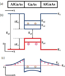
2.4.1.3 Delta (δ) Doping Layer
A uniformly doped supply layer can be replaced by an undoped supply layer,
followed by a very thin but extensively doped layer called a δ-doped layer (or
pulse-doped). Hence, when the parallel conduction problem in the barrier layer is reduced,
[image:42.595.141.461.205.459.2]high sheet charge density and breakdown voltage can be achieved.
Figure 2.11 Conduction band of general depletion mode HEMT structure
with -doping and bulk-doping [33]
As a result, the channel concentration increases. The difference of these doping to
the structure is illustrated in Figure 2.11. The energy quantization occurs at the
discontinuity formed between the high and low band gap materials. Electrons in the
supply layer (bulk doping case) or δ-doping can then tunnel through the thin
potential barrier and be trapped into the triangular QW. The electrons in the QW
forms a high electron mobility plane called a 2DEG. The Coulomb scattering
between electrons and the fixed ionized atoms separated by the spacer layer leads to
high mobility. Figure 2.12 shows the relation of -doping concentration and the drain
current as described in [41]. A degradation of the drain current is observed with
reducing the -doping concentration. Gate
metal
Supply Spacer 2
DEG
-doping
Bulk doping
Charge density
d1 d2 d3
qΦB
EF
EC
ΔEC
-
doping


![Figure 2.7 Energy and diagram of Schottky contact: (a) isolated and (b) on contact [33]](https://thumb-us.123doks.com/thumbv2/123dok_us/8764123.895506/37.595.135.530.179.394/figure-energy-diagram-schottky-contact-isolated-b-contact.webp)