BWW
9
Switching-aid Circuits
with Energy Recovery
Passive turn-on and turn-off snubber circuits for the IGBT transistor, the GCT and the GTO thyristor have
been considered in chapter 7. These snubber circuits modify the device I-V switching trajectory and in
so doing reduce the device transient losses. Snubber circuit action involves temporary energy stored in either an inductor or capacitor. In resetting these passive components it is usual to dissipate the stored energy in a resistor as heat. At high frequencies these losses (being proportional to frequency) may become a limiting factor because of the difficulties associated with equipment cooling. Instead of dissipating the switching-aid circuit stored energy, it may be viable to recover the energy back into the dc supply or into the load, or both. Two classifications of energy recovery circuits exist, either passive or
active. A passive recovery circuit involves only passive components such as L and C while active
recovery techniques involve extra switching devices, as in a switched-mode power supply, smps.
Figure 9.1. Conventional inductive turn-on snubber principal currents at: (a) turn-on and (b) turn-off.
9.1 Energy recovery for inductive turn-on snubber circuits – single ended
Figure 9.1 shows the conventional inductive turn-on snubber circuit for a single-ended IGBT transistor
switching circuit. Equally the switch may be a GCT or a GTO thyristor, for which an inductive turn-on
snubber is mandatory, if switch derating is to be avoided.
At switch turn-on the snubber inductance controls the rate of rise of current as the collector voltage falls to zero. The switch turns on without the stressful condition of simultaneous maximum voltage and
current (Vs,Im) being experienced. At turn-off the inductor current is diverted through the diode Ds and
Im Im
Rs
Ds
Chapter 9 Switching Aid Circuits with Energy Recovery 324
resistor Rs network and the stored inductor energy ½ 2
m
LI is dissipated as heat in the resistance of the
Ls-Rs-Ds circuit. The power loss is determined by the switching frequency and is given by½ 2 m s LI f . Full design and operational aspects of this turn-on snubber have been considered in chapter 8.3.3.
9.1.1 Passive recovery
i. Recovery into the dc supply
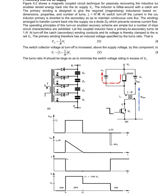
Figure 9.2 shows a magnetic coupled circuit technique for passively recovering the inductive turn-on
snubber stored energy back into the dc supply Vs. The inductor is bifilar-wound with a catch winding.
The primary winding is designed to give the required (magnetising) inductance based on core
dimensions, properties, and number of turns, L = N2/. At switch turn-off the current in the coupled
inductor primary is diverted to the secondary so as to maintain continuous core flux. The windings are
arranged to transfer current back into the supply via a diode DR which prevents reverse current flow.
The operating principles of this turn-on snubber recovery scheme are simple but a number of important circuit characteristics are exhibited. Let the coupled inductor have a primary-to-secondary turns ratio of
1:N. At turn-off the catch (secondary) winding conducts and its voltage is thereby clamped to the supply
rail Vs. The primary winding therefore has an induced voltage specified by the turns ratio. That is
1 (V)
p N s
VA = V (9.1)
The switch collector voltage at turn-off is increased, above the supply voltage, by this component, to
(
1 1)
(V)c N s
V = + V (9.2)
The turns ratio N should be large so as to minimise the switch voltage rating in excess of Vs.
Figure 9.2. Turn-on snubber with snubber energy recovery via a secondary catch winding:
(a) circuit diagram; (b) circuit waveforms; and (c) multilevel recovery.
1 N N N N Vs 0 (c) Cn C3 C2 C1 DR Ls Vs tft /N
At switch turn-on the inductor supports the full rail voltage and, by transformer action, the induced
secondary voltage is NVs. The reverse-blocking voltage seen by the secondary blocking diode DR is
(
1)
(V)c s
V = +N V (9.3)
Thus by decreasing the switch voltage requirement with large N, the blocking diode reverse voltage
rating is increased, and vice versa when N is decreased.
One further design compromise involving the turns ratio is necessary. The higher the effective pull-down voltage, the quicker the stored energy is returned to the dc supply. The secondary voltage during recovery is fixed at Vs; hence from v = L di/dt the current will decrease linearly from Im /N to zero in time
tft.By equating the magnetically stored primary energy with the secondary energy pumped back into the
dc rail source Vs 2 ½ m½ (J) p m s ft I L I V t N = (9.4)
The core reset time (and the switch minimum off-time), that is the time for the magnetic core energy to be returned to the supply, is given by
(s) m ft p s I t L N V = (9.5)
Thus the lower the turns ratio N, the shorter the core reset time and the higher the upper switching
frequency limit. Analysis assumes a short collector current fall time compared with the core reset time. Primary leakage inductance results in a small portion of the core stored energy remaining in the primary circuit at turn-off. This energy, in the form of primary current, can usually be absorbed and controlled by
the capacitive turn-off snubber circuit (R-C snubber) across the switch.
Figure 9.2c shows a recovery arrangement with multiple secondary windings, like the link arrangement
of a diode clamped multilevel inverter (Chapter 15.3). The reflected voltage,
(
1+N n V/)
s, on to theswitch is significantly reduced as the number of secondary windings, n, increases. Auto balancing and
regulation of the capacitor voltages is achieved since only the lowest charged (voltage) capacitor has energy transferred to it.
ii. Recovery into the load
Passive inductive energy recovery into the load tends not to significantly affect load voltage regulation since the recovered energy is related to the load current magnitude.
Figure 9.3 shows a passive inductor turn-on snubber with energy recovered into the load and the three recovery stages.
In figure 9.3b, at switch T turn-off, the inductor stored energy ½ 2
s m
L I is resonantly transferred to the
capacitor Cs in the path Ls-Ds -Cs. The switch is assumed to have a short turn-on time compared to the
resonant period. The capacitor Cs voltage and series resonant current are given by
( )
( )
cos sin m Co m i t I t V t I Z t ω ω ω ω = = (9.6)After time t=½π√LsCs the diode Ds blocks preventing continuation of resonance and the final capacitor
voltage is s Cs m m s L V I Z I C = = (9.7)
When switch T subsequently turns on, the energy stored in Cs is resonantly transferred to the
intermediate storage capacitor Co, through the path Cs-Lr-D -Co-T shown in figure 9.3c. All the energy in Cs is transferred provided Co > Cs, in which case the diode Dc across Cs conducts, clamping Cs to zero
volts. The final voltage on Co is
o s Co Cs m s o C L V V I C C = = (9.8)
During the transfer of energy from Cs to Co the circuit voltage and current waveforms are given by
equations (9.11) to (9.14). The voltage on Co given by (9.8) is retained until subsequent switch turn-off.
The final stage of recovery is shown in figure 9.3d where the capacitor Co dumps its charge at a
constant rate into the load as its voltage falls linearly to zero in a time, independent of the load current
Co Co o s o m V t C L C I = = (9.9)
during which time the capacitor Co voltage falls according to
( )
t0 m s m Co Co m o o o L I I V t V t I t C C C ω = = − = − (9.10)The load freewheel diode Df then conducts the full load current Im.
fsmps > fT fsmps Dsmps Lsmps Tsmps off on Db 0V 0V
see figure 9.26a
Co VCo
Figure 9.3. Inductive turn-on snubber with snubber energy recovery intermediate capacitors:
(a) circuit diagram; and successive (b) turn-off; (c) turn-on; and (d) turn-off.
9.1.2 Active recovery
i. Recovery into the dc supply
Figure 9.4 shows an inductive turn-on snubber energy recovery scheme which utilises a switched-mode power supply (smps) based on the boost converter in 15.4, and shown in figure 9.26a.
At switch turn-off the energy stored in the snubber inductor Ls is transferred to the large intermediate
storage capacitor Co via the blocking diode, Db. The inductor current falls linearly to zero in time Ls Im /
VCo. The smps is then used to boost the relatively low capacitor voltage into a higher voltage suitable for
feeding energy back into a dc supply. The capacitor charging rate is dependent on load current magnitude. The smps can be controlled so as to maintain the capacitor voltage constant, thereby fixing the maximum switch collector off-state voltage, or varied with current so as to maintain a constant snubber inductor reset time. One smps and storage capacitor can be utilised by a number of switching circuits, each with a blocking/directing diode as indicated in figure 9.4. The diode and switch are rated at
Vs+VCo. The smps is operated in a discontinuous inductor current mode in order to reduce switch and diode losses and stresses.
If the load and inductive turn-on snubber are re-arranged to be in the cathode circuit, then the
complementary smps in figure 9.26b can be used to recover the snubber energy from capacitor Co.
Figure 9.4. Turn-on snubber with active snubber inductor energy recovery.
Im Im L O A D Ls + + Lr T Dr Co Cs Ds Df Vs 0 Cs Lr Co + + Dr Co Im + Ls Cs Ds + (a) (b) (c) (d) Co>Cs D Dc Dc
Power Electronics
327
Figure 9.5. Conventional capacitive turn-off snubber showing currents at IGBT transistor:
(a) turn-off and (b) turn-on.
9.2 Energy recovery for capacitive turn-off snubber circuits – single ended
Figure 9.5 shows the conventional capacitive turn-off snubber circuit used with both the GTO thyristor
and the IGBT transistor. At turn-off, collector current is diverted into the snubber capacitor C via D. The
switch turns off clamped to the capacitor voltage which increases quadratically from zero. At the
subsequent switch turn-on the energy stored in C,½ 2
s
CV is dissipated as heat, mainly in the resistor R.
A full functional description and design procedure for the capacitive turn-off snubber circuit is to be found in chapter 8.3.1.
At high voltages and switching frequencies, with slow switching devices, snubber losses (½ 2
s s
CV f ) may
be too high to be readily dissipated. An alternative is to recover this energy (either into the load or back into the dc supply), using either passive or active recovery techniques.
Figure 9.6. A capacitive turn-off snubber with passive capacitor energy recovery into the load:
(a)with a capacitive turn-off snubber and (b) with an RC turn-off snubber.
Rs T Cs Ds L Co Do (a) (b) + + + + Df ON OFF + +
Chapter 9 Switching Aid Circuits with Energy Recovery 328
9.2.1 Passive recovery
i. Recovery into the load
Figure 9.6illustrates a passive, lossless, capacitive turn-off snubber energy recovery scheme which
dumps the snubber energy, ½ 2
s s
CV f , into the load. The switch turn-off protection is that with a
conventional capacitive snubber circuit.
At turn-off the snubber capacitor Cs charges to the voltage rail Vs as shown in figure 9.7a.
At subsequent switch turn-on, the load current diverts from the freewheeling diodeDf to the switch T.
Simultaneously the snubber capacitor Cs resonates its charge to capacitor Co through the path shown
in figure 9.7b,T - Cs - L - Do - Co.
When the switch next turns off, the snubber capacitor Cs charges and the capacitor Co discharges
into the load. When Co is discharged, the freewheeling diode conducts. During turn-off Co and Cs act
effectively in parallel across the switching device.
A convenient starting point for the analysis of the recovery scheme is at switch turn-on when snubber energy is transferred from Cs to Co.
Figure 9.7. Energy recovery turn-off snubber showing the energy recovery stages:
(a) conventional snubber action at turn-off; (b) intermediate energy transfer at subsequent switch turn-on; and (c) transferred energy dumped into the load at subsequent switch turn-off.
At switch turn-on
The active equivalent circuit portions of figure 9.7b are shown in figure 9.8a.
Analysis of the L-C resonant circuit with the initial conditions shown yields the following capacitor voltage
and current equations. The resonant current is given by
( ) Vssin (A) i t t Z ω = ω (9.11) 1 1 (ohms) (ohms) 1 (rad/s) 1 (rad/s) o o o o o o o s o n L Z L Z Z C n C n n LC C n C ω ω ω ω ω + = = = = + = = = where
The snubber capacitor voltage decreases from Vs according to
(
)
1 1 1 cos (V) 1 Cs s V V t n ω = − + − (9.12)while the transfer capacitor voltage charges from zero according to
(
1 cos)
(V) 1 Co s n V V t n ω = − + (9.13) + + T TFigure 9.8. Equivalent circuit for the intermediate energy transfer phase of snubber energy recovery, occurring via: (a) the main switch T and (b) then via the snubber diode Ds.
Figure 9.9. Circuit waveforms during intermediate energy transfer phase of snubber energy recovery: (a) transfer capacitor C0 current; (b) snubber capacitor voltage; and (c) transfer capacitor voltage.
Examination of equation (9.12) shows that if n > 1, the final snubber capacitor Cs voltage at ωt = π will be positive. It is required that Cs retains no charge, ready for subsequent switch turn-off; thus n ≤ 1, that is Co ≥ Cs. If Co is greater than Cs equation (9.12) predicts Cs will retain a negative voltage. Within the
practical circuit of figure 9.6, Cs will be clamped to zero volts by diode Ds conducting and allowing the
remaining stored energy in L to be transferred to Co. The new equivalent circuit for ωt =cos−1
( )
−n isshown in figure 9.8b. The resonant current, hence transfer capacitor voltage are given by
(
)
(
)
( ) sin (A) cos (V) s o o Co s o V i t t Z V n V t ω ω φ ω φ = + = + (9.14)where t≥ 0 and tan1 1n2
n
φ= − − − .
In maintaining energy balance, from equation (9.14) when the inductor L current i(ωt) =0, the final
voltage on Co is n Vsand Cs retains no charge, VCs =0.
The voltage and current waveforms for the resonant energy transfer stage are shown in figure 9.9. equation (9.12)
equation (9.13) equation (9.11)
equation (9.14)
At switch turn-off
Energy dumping from Co into the load and snubber action occur in parallel and commence when the
switch is turned off. As the collector current falls to zero in time tfia number of serial phases occur.
These phases, depicted by capacitor voltage and current waveforms, are shown in figure 9.10.
Phase one
Capacitor Co is charged to n Vs, so until the snubber capacitor Cs charges to
(
1− n V)
s, Co isinactive. Conventional snubber turn-off action occurs as discussed in chapter 8.3.1. The snubber capacitor voltage increases according to
2 ½ m (V) Cs s fi I V t C t = (9.15)
while Co remains charged with a constant voltage of n Vs. This first phase is complete at to when
(
)
2 ½ m o 1 (V) Cs o s s fi I t V v n V C t = = = − (9.16) whence(
)
2 1 (s) s s fi o m nV C t t I − = (9.17)and the collector current
(
1)
(A)o m totfi
I =I − (9.18)
Figure 9.10. Circuit waveforms at switch turn-off with turn-off snubber energy recovery when:
(a) the snubber Cs is fully charged before the switch current at turn-off reaches zero and
(b) the switch collector current has fallen to zero before the snubber capacitor has charged to Vs.
Phase two
When Cs charges to
(
1− n V)
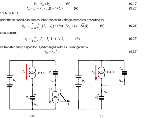
s, the capacitor Co begins to discharge into the load. The equivalent circuitis shown in figure 9.11a, where the load current is assumed constant while the collector current fall is assumed linear. The following Kirchhoff conditions must be satisfied
Power Electronics 331 + + + + (V) s Cs Co V =V +V (9.19) (1 / ) (A) m Co Cs o fi I =i +i +I −t t (9.20) for 0 ≤ t≤tfi –to
Under these conditions, the snubber capacitor voltage increases according to
(
)
2(
)
1 ½ / 1 (V) 1 Cs m o o s s n V I I t t t n V n C = − + + − + (9.21) with a current{
}
1 (1 / ) (A) 1 Cs m o o i I I t t n = − − + (9.22)The transfer dump capacitor Co discharges with a current given by
/ Co Cs
i =i n (9.23)
Figure 9.11. Turn-off snubber equivalent circuit during energy recovery into the load when:
(a) Co begins to conduct and (b) after the switch has turned off.
Phase three
If the snubber capacitor has not charged to the supply rail voltage before the switch collector current has reached zero, phase three will occur as shown in figure 9.10b. The equivalent circuit to be analysed is shown in figure 9.11b. The Kirchhoff equations describing this phase are similar to equations (9.19) and (9.20) except that in equation (9.20) the component Io(1-t/t0) is zero.
The capacitor Cs, charging current is given by (A) 1 Cs m n i I n = + (9.24)
while the dumping capacitor Co current is
/ (A)
Co Cs
i =i n (9.25)
The snubber capacitor charges linearly, according to (V) 1 m Cs io s I n V v t n C = + + (9.26)
When Cs is charged to the rail voltage Vs, Co is discharged and the load freewheeling diode conducts the
full load current Im.
Since the snubber capacitor energy is recovered there is no energy loss penalty for using a large snubber capacitance and the larger the capacitance, the lower the switch turn-off switching loss. The
energy to be recovered into the load is fixed, ½ 2
s s
C V and at low load current levels the long discharge
time of Co may inhibit proper snubber circuit action. This is generally not critical since switching losses
are small at low load current levels. Output voltage regulation is reduced, since the amount of energy recovered into the load is independent of the load current.
ii. Recovery into the dc supply
Figure 9.12 show two turn-off snubber circuits where the energy is recovered back into the dc supply. The ac circuit operational mechanisms are the same for both circuits.
When the switch T is turned off the snubber capacitor Cs charges to the dc rail voltage Vs.
Chapter 9 Switching Aid Circuits with Energy Recovery 332
Figure 9.12. A capacitive turn-off snubber with passive energy recovery into the supply:
(a) basic capacitive turn-off snubber and (b) an alternative configuration.
At switch T turn-on, the snubber capacitor Cs resonates with inductor Lr through the coupled transformer
primary Lp, in the loop Cs -Do –Lp -Lr -T, returning energy to the dc supply through the coupled
secondary circuit. The primary voltage is Vs /N, and provided this referred voltage is less than a half Vs,
all the energy on Cs is transferred to the dc supply via the transformer. The snubber diode Ds clamps the
capacitor Cs voltage to zero, and excess energy in Lr is transferred to the dc supply, in the loop Do – Lp
-Lr – Ds, as the inductor Lr current falls linearly to zero when opposed by the referred dc link voltage via
the transformer. In figure 9.12a, the secondary winding can be connected to the other terminal of Cs.
Once the energy transfer is complete, the transformer core magnetising current resets to zero in the same Kirchhoff loop, but at a low voltage. Reset must be complete in one complete period of switch T.
iii RC snubber recovery
The IGCThyristor is commonly used and characterised with an RC snubber. The figure 9.6b shows how
the snubber diode Ds in figure 9.6a can be replaced by a resistor to form an RC snubber, provided diode
Ds is used to clamp the minimum snubber capacitor voltage to zero. The resistor losses are ½CsV2
. The
snubber capacitor stored energy after turn-off, ½CsV2
, can be recovered at switch turn-on, provided the
RsCs time constant is at least comparable with the LC resonant period – an unlikely condition.
9.2.2 Active recovery
i. Recovery into the dc supply
Active energy recovery methods for the turn-off snubber are simpler than the technique needed for active recovery of turn-on snubber circuit stored energy. This is because the energy to be recovered
from the turn-off snubber is fixed at ½ 2
s s
C V and is independent of load current. In the case of the turn-on
snubber, the energy to be recovered is load current magnitude dependent ( 2
L I
α ) which complicates
active recovery. Active turn-off snubber energy recovery usually involves an intermediate capacitive energy storage stage involving a positive or negative voltage rail (with respect to the emitter of the principal switch).
a Negative intermediate voltage rail
At switch T turn-on the snubber capacitor stored energy is resonated into a large intermediate storage
capacitor Co as shown in figure 9.13a. Recovery from Cs to Co at switch T turn-on occurs through the
following loops:
at switch T turn-on when VCs > 0: Cs -T- Co - L- Da (as shown in figure 9.8a and equations (9.12) - (9.13)) then when VCs = 0: Ds - Co - L- Da (as shown in figure 9.8b and equation (9.14))
The switch current is increased by the resonant current, which has a maximum of VCo/ L C/ s. It is
possible to use the energy in Co as a negative low-voltage rail supply. This passive recovery technique
suffers from the problem that the recovered energy ½ 2
s s
C V may represent more energy than the
low-voltage supply requires. An independent buck-boost smps can convert excess energy stored in Co to a
more useful voltage level. Producing the gate drive for the smps switch Tsmps presents few difficulties
since the gate-emitter has a low dc offset and does not experience any dv/dt relative to the emitter
reference voltage of the main switch T.
(a) (b) Vs Im on Df/b Lr Do 1:N Ds L O A D Cs + T 0 Df on Im on L O A D on Df/b Ds Lr Do Vs 1:N + Cs T 0 Df N>2 Lp Ls Lp Ls
The basic recovery circuit, with the buck-boost smps, can form the basis of an active turn-off snubber energy recovery circuit when switches are series connected, as considered in section 9.4.
It may be noticed that the ‘Cuk’ converter in chapter 17.6 is in fact the snubber energy recovery circuit in figure 9.13a, controlled in a different mode.
Figure 9.13. Switching circuit for recovering turn-off snubber capacitor energy,
and for providing either (a) a negative voltage rail and/or transferring to Vs, via a buck-boost smps
or (b) a positive voltage rail and/or transferring to Vs, via a boost smps. b Positive intermediate voltage rail
A positive voltage source, with respect to the main switch emitter, can be produced with the recovery circuit in figure 9.13b. Practically, an extra switch, Trev, is needed in order to minimise the time of current
decay in the loop L - Ds, after the switch T is turned on and the voltage on the snubber capacitor Cs has
resonated to zero. A passive resistor-capacitor network can be used to synchronise the turn-on (due to
the main switch T turning on) and turn-off (due to diode Ds becoming forward biased) of the low-voltage
switching device Trev. Recovery from Cs to Co at switch T turn-on occurs through the following Kirchhoff
current loops:
at switch T turn-on when Trev is on and VCs > 0: Cs -T - L - Trev for a period ½π√LCs
then when Trev is off and VCs = 0: Co - L - Da for a period Vs /ωoVCo
A boost smps controls and transfers the energy on Co to the dc rail through diode Dsmsp.
The basic recovery circuit, with the boost smps, when cascade connected, can form the basis of an active turn-off snubber energy recovery circuit for series connected switches, as considered in 9.4.
ii. RC snubber recovery
The IGCThyristor is commonly used and characterised with an R-C snubber (as opposed to a parallel
connected series capacitor-diode turn-off snubber). The insert in figure 9.13a, for use in figures 9.13a
and b, shows how the snubber diode Ds can be replaced by a resistor to form an R-C snubber, provided
diode Dc is used to clamp the minimum snubber capacitor voltage to zero. The resistor losses are
½CsV2
. Most of the snubber capacitor stored energy after turn-off, ½CsV2
at switch turn-off, (depending
on the Rs-Cs time constant), can be recovered using either of the basic circuits in figure 9.13, or the
circuits in figures 9.6 and 9.14, provided the RsCs time constant is greater than the LC resonant period.
T Lsmps Dsmps off on Tsmps SMPS SMPS Im off on Df L Vs Ds Cs Co + Lsmps Vs Dsmps Tsmps Trev off on L O A D + (a) (b) on Da 0V Rs T Cs Dc L Da
Whether a positive or negative intermediate voltage is produced on Co, (typically a few tens of volts, but
much higher if part of a turn-on snubber recovery circuit), the energy on Co is usually smps converted to
stable gate voltage levels of the order of ±15V. Since a dual rail polarity gate level supply is needed, the polarity of the voltage on Co (viz., positive or negative) is inconsequential.
9.3 Unified turn-on and turn-off snubber circuit energy recovery – single ended
9.3.1 Passive recovery
Conventional inductive turn-on and capacitive turn-off snubber circuits can both be incorporated around a switching device as shown in figure 8.20 where the stored energy is dissipated as heat in the reset resistor. Figure 9.14 shows unified turn-on and turn-off snubber circuits which allow energy recovery from both the snubber capacitor Cs and inductor ℓs.
i. Recovery into the load
The snubber capacitor energy is recovered by the transfer process outlined in section 9.2.1. Figure
9.14a shows the energy transfer (recovery) paths at switch turn-off. The capacitor Co and inductor ℓs
transfer their stored energy to the load in parallel and simultaneously, such that the inductor voltage is
clamped to the capacitor voltage VCo.
As Co discharges, the voltage across ℓs decreases to zero, at which time the load freewheel diode Df
conducts. Any remaining inductor energy is dissipated as unwanted heat in circuit resistance. Proper
selection of ℓs and Cs (½ 2 ½ 2
s m s s
L I ≤ C V ) can minimise the energy that is lost although all the snubber
capacitor energy is recovered, neglecting diode and stray resistance losses. The energy (controlled by,
and transferred to the turn-on snubber inductor ℓs) associated with freewheel diode reverse recovery
current, is also recovered.
Figure 9.14. Switching circuits incorporating unified turn-on and turn-off snubber,
showing recovery path of energy (a) in Co and ℓs; (b) in Cs and ℓs through Dr.; and
(c) recovery circuit when an RC snubber is employed.
At switch turn-on
When the switch is off, the freewheel diode Df conducts the load current Im, capacitor voltage VCs = Vs
and VCo =0.
Phase one: 1 on P t
When the switch is turned on, the series inductor ℓs performs the usual turn-on snubber function of
controlling the switch di/dt according to (assuming the switch voltage fall time is relatively short)
( )
ss V
i t = t
A (9.27)
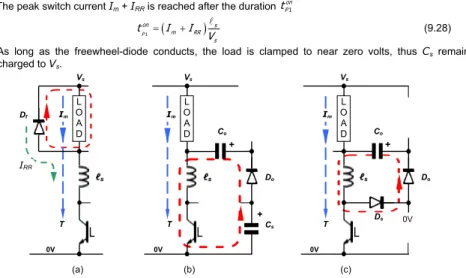
The switch current rises linearly to the load current level Im and then continues to a level IRR higher as
the freewheel diode Df recovers with currents in the paths shown in figure 9.15a. This diode reverse
recovery current IRR is included in the analysis since the associated energy transferred to the turn-on
inductor is subsequently recovered.
(a) (b) + Df Df on on Df/b Dc Co Do DR 1:N + + Rs T Cs Ds ℓs Co Do Da (c) Do Lo Vs D1
Power Electronics
335
The peak switch current Im + IRR is reached after the duration 1 on P t
(
)
1 P on s m RR s t I I V = + A (9.28)As long as the freewheel-diode conducts, the load is clamped to near zero volts, thus Cs remains
charged to Vs.
Figure 9.15. Unified turn-on and turn-off snubber at switch turn-on, showing (a) current build-up in
ℓs; (b) energy resonant transfer from Cs to Co; and (c) energy transfer from ℓs to Co through Ds.
Phase two: 2 on P t
The turn-off snubber capacitor Cs charge resonates in the path Cs - Do - Co - ℓs and through the switch T,
as shown in figure 9.15b. The capacitor voltages and resonant current are given by (n=Cs/Co)
( )
( )
ssin cos Cs Co RR V i t i t t I t Z ω = ω = ω + ω (9.29)( )
1 1(
1 cos)
sin 1 o Cs s RR Z V t V t I t n n ω ω ω ω ω = − − + + (9.30)( )
(
1 cos)
sin 1 o Co s RR n V t V t Z I t n ω ω ω ω ω = − + + (9.31) 1 1 (ohms) (ohms) 1 1 (rad/s) (rad/s) s s s o o o o o o o s o C n Z Z Z n C n C C n n C ω ω ω ω ω + = = = = = + = = where A A A The freewheel diode Df voltage is( )
(
1 cos)
sin Df s Co Cs s RR V t V V V V t I Z t ω ω ω = + − = − + (9.32)When the freewheel-diode current reaches its peak recovery level, IRR, it is able to support a voltage
which from equation (9.32) sinusoidally increases from zero. Specifically the freewheel-diode reverse
bias VDf is controlled such that zero voltage turn-off occurs resulting in low recovery power losses. Stray
or inductance deliberately introduced in series with Do (to decrease the resonant peak current given by
equation (9.29), approximatelyVs /Z) produces a freewheel-diode recovery step voltage Vs ℓs /(ℓs +
Lstray), where the step is always less than Vs.
The resonant period prematurely ends (since n < 1) when the snubber capacitor Cs voltage reduces to
zero and is clamped to zero by conduction of the snubber diode Ds, as shown in figure 9.15c. Assuming
IRR=0 (to obtain a tractable solution), equating equation (9.30) to zero yields the time for period 2, 2
on P t , that is
( )
2 1 P on cos n t ω − − = (9.33) at which time( )
2(
)
2 1 P on s Co V i t n Z = − (9.34) L O A D ℓs Co Do T Im Vs 0V Ds L O A D ℓs Co Cs Do T Im Vs 0V L O A D ℓs T Df Im Vs 0V (a) (b) (c) IRR 0V + + +Chapter 9 Switching Aid Circuits with Energy Recovery 336
and
( )
P2 on Co s V t =nV (9.35) Phase three: tPon3The remaining energy stored in ℓs is resonantly transferred into Co in the path Do - Co - ℓs - Ds, with initial
conditions given by equations (9.34) and (9.35), according to
( )
sin(
)
Co o s o V ωt = n V ωt+φ (9.36) and( )
scos(
)
o o o V i t n t Z ω = ω +φ (9.37)The resonant current reaches zero and energy transfer to Co is complete, after a period
3 ½ on P o t π φ ω − = (9.38)
If the diode reverse recovery energy is reintroduced, based on energy transfer balance, the final voltage on Co is
( )
2(
)
2 3 on P Co t s o RR V = nV + Z I (9.39)The on equations (9.29) to (9.37) are essentially the same as equations (9.11) to (9.14) for the turn-off snubber energy recovery circuit considered in section 9.2.1, except free-wheel diode reverse recovery has now been included. The circuit turn-on voltage and current waveforms shown in figure 9.9 are also applicable.
At switch turn-off
When the switch is on, it conducts the load current Im and the snubber capacitor Cs voltage is zero,
while the transfer capacitor voltage VCo( 3
on P
t ) =√n Vs = Vo (neglecting the IRR component) is a result of
the previous switch turn-on. When the switch T is turned off, the collector current decreases linearly from
Im towards zero in time tfi.
Figure 9.16. Unified turn-on and turn-off snubber at switch turn-off, showing (a) current diversion to
snubber capacitor Cs; (b) transfer capacitor Co releasing energy (c) energy transfer to the load
simultaneously from ℓs and Co through DR; and (d) energy transfer from Co into the load through DR.
Phase 1: 1 off P t
The load current is progressively diverted to the snubber capacitor as the collector current decreases, giving a capacitor (and collector) voltage of
( )
(
)
2 0 0 1 1 0 2 t t m ce Cs m c m fi s s fi s fi I t t v V t I i dt I dt t t C C t C t = =∫
− =∫
= ≤ ≤ (9.40)If the collector current reaches zero before any other associated recovery processes occurs, then after the collector current has reached zero, the collector and snubber voltages rise linearly (being clamped in parallel), with currents in the paths shown in figure 9.16a, according to
L O A D ℓs Cs T Df Im Vs 0V Ds ℓs Co Cs DR T Df Im Vs 0V Ds L O A D L O A D ℓs Co Do DR T Df Im Vs 0V Ds L O A D Co DR T Df Im Vs 0V (a) (b) (c) (d) + + + + +
( )
½ m fi m provided ½ m fi ce Cs s o s s s I t I t I t v V t V V C C C = = + ≤ − (9.41)The collector voltage reaches Vs at a time given from equation (9.41) when VCs = Vs – VCo as
(
)
1 ½ off s P s o fi m C t V V t I = − + (9.42)where Vo is given by equation (9.39) and the period duration includes the collector linear fall period tfi.
Phase 2: 2 off P t
When the collector (and snubber) voltage VCs reaches Vs -Vo capacitor Co begins to discharge into the
load providing the load current Im. Simultaneously Cs charges to Vs throughℓs, as shown in figure 9.16b.
The relevant circuit capacitor voltages and current are
( )
1 1cos 1 s m n i t I t n n ω = + ω + A (9.43)( )
1 1 sin 1 1 Cs m o o s o V t I Z t t V V n n ω = ω +ω + − + + (9.44)( )
1 1 sin 1 1 Co m o o o V t I Z t t V n n ω = ω −ω + + + (9.45)This phase is complete when the snubber capacitor Cs is charged to the supply voltage, Vs, assuming
the inductor current is greater than zero at that time. Let the inductor current be I2 at the end of the
off-period tPoff2and the capacitor Co voltage be V2. Phase 3: 3
off P t
The snubber capacitor is clamped to the rail voltage. The transfer capacitor Co and snubber inductor ℓs
both release energy in parallel into the load through the paths shown in figure 9.16c. The inductor
voltage is clamped to the capacitor Co voltage. The snubber inductor current is
( )
2(
)
2 sin cos s o m o m o o V i t I t I I t Z ω = + ω + − ω A (9.46)while the transfer capacitor voltage is
( )
2cos(
2)
sinCo o o o m o
V ωt =V ωt+Z I −I ωt (9.47)
One of two conditions form the completion of this phase
• the transfer capacitor voltage reaches zero before the snubber inductor current reaches zero
• the snubber inductor current reaches zero before the transfer capacitor voltage reaches zero
The first condition represents the case where the remaining inductor current associated energy is lost as it freewheels to zero in the low voltage path ℓs - Do - DR and the load.
In the second case, the inductor current given by equation (9.46) reaches zero, while the transfer
capacitor Co continues to discharge into the load as shown in figure 9.16d. The inductor current is
prevented from reversing by diode Ds. Once the inductor current has fallen to zero, the transfer capacitor
voltage falls linearly to zero as it provides the load currentIm. This second case represents the situation
when 100% of all snubber (inductor ℓs and capacitor Cs) and diode reverse recovery energy is
recovered, that is
(
)
2 2½As Im+IRR ≤½C Vs s (9.48)
Snubber reset and recovery is complete when the snubber inductor current and transfer capacitor
voltage are both zero, the collector voltage has ramped to Vs, and the free-diode conducts the full load
current Im. From equation (9.47), this stage is complete when VCo( 3
off P t ) =0, that is
(
)
1 2 3 2 1 tan off P o o m V t Z I I ω − = − (9.49)Now the switch can be turned on.
ii. RC-L dual snubber recovery
The IGCThyristor is commonly used and characterised with an RC snubber and an inductive turn-on
snubber. Figure 9.14c shows how the snubber diode Ds in figure 9.14a can be replaced by a resistor to
form an RC snubber, provided diode combination Da -Ds is used to clamp the minimum snubber
capacitor voltage to zero. The resistor losses are ½CsV2
. The snubber capacitor stored energy after turn-off, ½CsV2
, can be recovered at switch turn-on, while the inductive turn-on energy ½LsI2
is
recovered at switch turn-off, provided the RsCs time constant is greater than the LC resonant period.
iii. Recovery into the load and supply
Figure 9.14b shows a dual snubber energy recovery technique where a portion of the resonance energy is transferred back to the dc supply (as opposed to the load) at switch turn-on, through a magnetically coupled circuit where it is required of the turns ratio that N >2. This reduces the energy transferred from the snubbers to the load, giving better load regulation under light load conditions. Load regulation with
light loads is poor since the snubber capacitor energy is fixed, ½ 2
s s
C V , independent of the load, Im. In
the analysis to follow, the recovery contribution of freewheel diode reverse recovery energy is neglected.
At switch turn-on
The turn-on phase is essentially the same as the circuit considered in figure 9.14a, except the
transformer is seen as an opposing emf voltage source Vs /N.
Phase one: 1 on P t
The switch current fall period is described by equation (9.27) and the time of the first turn-on period is given by equation (9.28).
Phase two: 2 on P t
The equations (9.29) to (9.35) are modified to account for the transformer referred voltage Vs /N
( )
( )
( )
1 ssin s Cs Co V N i t i t i t t N Z ω = ω = ω = − × ω A (9.50)( )
(
1)
1(
1 cos)
1 Cs s V t V Nn N t N n ω = × × + + − ω + (9.51)( )
(
(
1)
) (
1 cos)
1 Co s n N V t V t N n ω = − − ω + (9.52)The instantaneous power being returned to the supply through the transformer is given by
( )
( )
2 2 1 1 sin s sin s s s s V V V N V N p t i t t t N N N Z N Z ω = ×A ω = × − × ω = − × ω (9.53)The time for this period is given by equation (9.51), when the snubber capacitor voltage is zero 2 1 1 1 1 P on nN t cos N ω − + = × − − (9.54)
The energy returned to the supply is
( )
½( )
2 2 2 2 1 1 since 2 J P on s Trans s s s s V n w t C V C V N N ωZ N + = × = × < > (9.55) Phase three: 3 on P tEnergy continues to be recovered back into the supply Vs through the transformer when the resonant
current transfers to the diode Ds. Capacitor Cs charges to Vs and is clamped to Vs by diode Dc. The final voltage on the transfer capacitor Co is
( )
2 3 1 1 on s P Co V t V nN N = + − (9.56)The total energy transferred to the supply through the transformer is the difference between the initial energy in ℓs and Cs and the final energy in Co.
(
2 3)
2 2 2 2 2 2 ½ ½ ½ s 1 1 P P on on Trans s s s m o V w t t C V I C nN N + = + A − + − (9.57)If the turn-on inductor current reaches zero before the third phase can commence (due to N being too
small), then the turn-off snubber does not fully discharge, and will act as a soft clamp in the subsequent switch turn-off cycle. The capacitors retain the following voltages
(
)
(
)
2 2 1 1 Cs s s s Nn N V V V V N n N n + − = = − − − (9.58)(
)
(
)
2 1 1 Co s n N V V N n − = + (9.59) At switch turn-offThe circuit recovery operation at turn-off is essentially the same as when no transformer is used (N→∞),
except that the voltage on Co at the begin of turn-off is given by equation (9.59) or equation (9.56), as
Power Electronics
339
Operating regions of the dual energy recovery circuits
Both the passive unified recovery circuits analysed can be assessed simultaneously for their operational
bounds, since the bounds for the transformerless version in figure 9.14a are obtained by setting N to
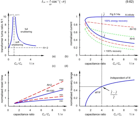
infinitely in the appropriate equations for the recovery circuit in figure 9.14b. Figure 9.17 shows various operational boundaries for the two unified passive energy recovery circuits analysed. The various boundaries are determined from the operating equations for the circuits.
The boundaries in figure 9.17a show the regions of full snubbering and for soft snubbering where the
capacitor Cs is not reset to zero voltage during the resonant cycles at turn-on. The boundaries are
summarised as follows 2 N n N − < (9.60) 2 N n N < − (9.61)
The boundaries in parts b and d of figure 9.17 satisfy equation (9.57), namely the capacitor energy is
less than the inductor energy. The current is normalised with respect to √nVs / Zo. Part d shows that the
relative range for 100% recovery, defined as (I I−∨) /I, is independent of the transformer turns ratio.
Figure 9.17c shows the normalised (with respect to 2π√n/ωo) reset time at turn-off. The reset time at
turn-on is the sum of periods one and two, but is dominated by the second turn-on period, namely
( )
1 1 cos on t n ω ∨ − = − (9.62)Figure 9.17. Unified, passive snubbering characteristics:
(a) operating regions with recovery transformer; (b) 100% recovery regions with different transformer turns ratios; (c) normalised circuit reset limits; and
(d) normalised recovery range independent of transformer turns ratio.
0 2 4 Co /Cs 1/n tr ans fo rm er t u rn s ra ti o N :1 10 8 6 4 2 0 full snubbering soft snubbering n>1 n>1 N =2 0 2 4 6 8 10 capacitance ratio Co /Cs 1/n n o rm a lis e d c u rr e n t 1 0.8 0.6 0.4 0.2 0 < 100% recovery N infinite N=10 N=4 100% energy recovery 0 2 4 6 8 10 capacitance ratio Co /Cs 1/n n o rm a lis e d re se t ti m e 4 3 2 1 0 N=2 max N=100 max min min 0 2 4 6 8 10 capacitance ratio Co /Cs 1/n n o rm a lis e d re co ve ry ra n g e 0.8 0.6 0.4 0.2 0 all N Independent of N (a) (b) (c) (d) I I∨ I I I ∨ − Fig 9.14a
Chapter 9 Switching Aid Circuits with Energy Recovery 340
9.3.2 Active recovery i. Recovery into the dc supply
Both turn-on and turn-off snubber energy can be recovered into the dc supply using a dedicated
buck-boost smps formed by Tsmps, Dsmps and Lsmps, shown in figure 9.18. Both snubbers (capacitor Cs and
inductor Ls) transfer their energy to the intermediated storage capacitor, Co, from which the energy is
smps transferred to the dc supply Vs. The buck-boost smps also maintains a fixed voltage on Co, which
facilitates rapid energy transfer of the turn-on snubber inductor Ls energy to Co at switch T turn-off, in
time LsIm / VCo. The maximum switch off-state voltage is Vs+VCo. At switch T turn-on, the turn-off snubber capacitor Cs energy is resonated to Co through the loop Cs-T-Co - Ls-Do, as considered in detail in section 9.3.1. The smps is operated in a discontinuous inductor current mode in order to minimise smps
switch and diode losses and stresses. The maximum smps switch and diode voltages are Vs+VCo.
Figures 9.18b and c show circuit versions with a reduced component count. With the inductor ℓ removed,
the resonant reset current magnitude and period is now only controlled by the turn-on snubber inductor. A further diode can be removed as shown in figure 9.18c, but the number of series components in the turn-on inductor reset path is increase as is the loop inductance associated with the path.
Figure 9.18. Unified, active turn-on and turn-off snubber energy recovery circuits:
(a) basic circuit and (b) and (c) reduced component variations.
9.4 Inverter bridge legs
Capacitive turn-off snubbers (without any turn-on snubber circuit inductance), both active and passive are not normally viable on bridge legs because of unwanted capacitor discharging and subsequent uncontrolled charging current, as considered in chapter 8.4. At best capacitive soft turn-off voltage
clamps (operational at >Vs) can be employed to reduce turn-off losses, as shown in figure 8.24.
9.4.1 Turn-on snubbers
i. Active recovery - recovery into the dc supply
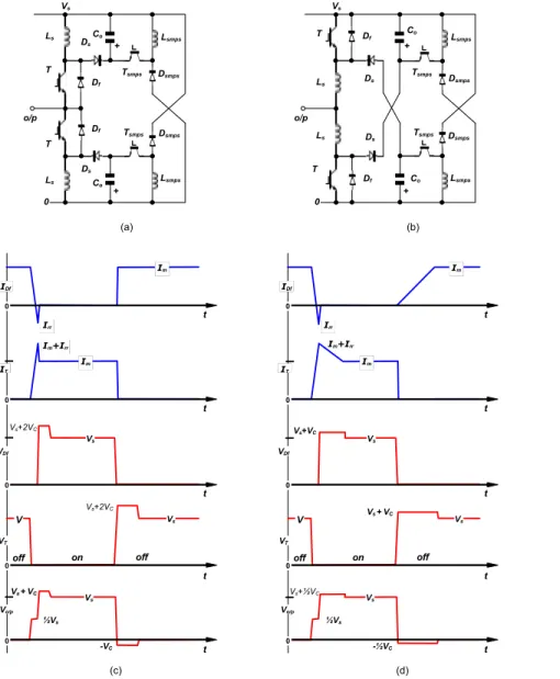
Figure 9.19 shows inverter bridge legs where both switches benefit from inductor turn-on snubbers and active energy recovery circuits. The circuits also recover the energy associated with freewheel diode reverse recovery current. The turn-on energy and diode recovery energies are both recovered back into
the dc supply, Vs, via a buck-boost smps. At switch turn-off, the energy stored in Ls is transferred to
capacitor Co via diode Ds.
For given turn-on snubber inductance Ls, both circuits give the same di/dt in the switches. The capacitor
voltages determine the snubber reset time. When both circuits result in the same switch maximum voltages, the reset times are the same. But the capacitor voltages in figure 18.9a are half those for the circuit in figure 9.19b. The main operational difference between the two configurations is the periods when the capacitors are charged. In figure 9.19a, both capacitors are charged at both switch turn-on and turn-off. In figure 9.19b, each capacitor charges once per cycle, one capacitor is charged at turn-on, the other at turn-off.
Coupling of the turn-on inductors results in virtual identical waveforms as to when the inductors are not magnetically coupled. No net energy savings or gains result. Close coupling is therefore not necessary.
ℓ Vs 0 Tsmps Dsmps Lsmps Co Cs Ds Df T Ls + + Im Df Do off on Vs 0 Tsmps Dsmps Lsmps Co Cs Ds Df T Ls + + Im Df Do Vs 0 Tsmps Dsmps Lsmps Co Cs Ds Df T Ls + + Im Df Do (a) (b) (c)
Figure 9.19. Active inductive turn-on snubber energy recovery circuits: (a) multiple single-ended circuit; (b) cross-coupled high frequency circuit; and (c) and (d) respectively circuit waveforms.
9.4.2 Turn-on and turn-off snubbers
i. Passive recovery - recovery into the dc supply
Figure 9.20 shows an inverter bridge leg where both switches have inductor on and capacitor turn-off snubbers and passive energy recovery circuits. The circuit also recovers the energy associated with freewheel diode reverse recovery current. Both the turn-on energy and turn-off energy are recovered
back into the dc supply, Vs. Although this decreases the energy transfer efficiency, recovery into the
(a) (b) Vs 0 Tsmps Dsmps Lsmps Co o/p Ds Df T Ls + + Df Ls Tsmps Lsmps Co Dsmps T Ds Vs 0 Tsmps Dsmps Lsmps Co o/p Ds Df T Ls + + Df Ls Tsmps Lsmps Co Dsmps T Ds 0 Im t Vs Im Irr Im+Irr 0 0 0 0 t t t t Vs Vs V Vs+2VC Vs+2VC Vs +VC ½Vs IDf IT VDf VT Vo/p on off off -VC 0 Im t Vs Im Irr Im+Irr 0 0 0 0 t t t t Vs Vs V Vs +VC Vs+VC Vs+½VC ½Vs IDf IT VDf VT Vo/p on off off -½VC (c) (d)
load gives poor regulation at low load current levels where the capacitor turn-off energy, which is fixed, may exceed the load requirements. Energy recovery involves a coupled magnetic circuit which can induce high voltage stresses across semiconductor devices. Such conditions can be readily avoided if a split capacitor (multilevel) voltage rail, fed from multiple secondaries, is used, as shown in figure 9.2c. Dual snubber (inductor and capacitor) energy recovery occurs as follows.
For switch S1, the turn-off snubber is formed by CS1 and DS1, and the turn-on snubber comprises LS1.
1. The energy stored in CS1 is resonantly transferred to Co1 when switch S1 is switched on, in the
path CS1 - Dt1 - Co1 - LS2 - LS1 -S1.
2. The energy stored on Co1 is resonantly transferred to the dc supply Vs through transformer T1
when switch S1 is turned off and (after an underlap period) S2 is turned on (in the path Co1
-Lr1 -T1 -S2).
3. When S2 is turned on, the turn-on snubber inductor LS1 releases its energy in parallel with
capacitor Co1 (in the path LS1 - Ds1 – Dt1 - Lr1 -T1 -S2 - LS2).
4. The diode Dr1 prevents (by clamping) the transfer capacitor Co1 from reverse charging, by
providing an alternate path for the remaining energy in the resonant inductor Lr1 to be
returned to Vs via the coupling transformer T1.
5. The transformer T1 magnetising current is also returned to the dc supply Vs, thereby
magnetically resetting the coupling transformer T1.
The numerical subscripts ‘1’ and ‘2’ are interchanged when considering the recovery processes
associated with switch S2.
The recovery circuit can operate at switching frequencies far in excess of those applicable to the
IGCThyristor and the high power IGBT. The limiting operational factor tends to be associated with the
various snubber reset periods which specify the switch minimum on and off times. Although adequate for IGCThyristor requirements, minimum on and off times are a restriction to the IGBT.
Figure 9.20. Unified, passive snubber energy recovery circuits for GTO and GCT inverter bridge legs.
ii. Active recovery - recovery into the dc supply
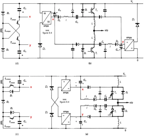
Figure 9.21 shows two similar turn-on and turn-off snubber, active energy recovery circuits, which are particularly suitable for bridge leg configurations. In figure 9.21a, the turn-on snubber section is similar in operation to that shown in figure 9.4 while the turn-off snubber section is similar in operation to that shown in figure 9.13a. A common buck-boost smps is used for each turn-on and turn-off snubber pair. This arrangement is particularly useful when the two power switches and associated freewheel diodes are available in a single isolated module package.
The active recovery circuit in figure 9.21b shows the inductive turn-on snubbers relocated. The buck-boost smps inputs are cross-coupled, serving the turn-on snubber of one switch and the turn-off snubber of the other switch.
+
+ +
Power Electronics 343 see figure 9.3 see figure 9.4 Co Co Co Co Cs Dr Dr Dr Dr Lsmps + + Lsmps Tsmps Dr Tsmps Co Co (c) Di Di Lsmps + + Tsmps Dr Tsmps Co Co Dr (d) see figure 9.4 x y x y x y x y
The interaction of turn-off snubbers in both circuits can create high L-C resonant currents as discussed
in section 8.4. In each case, two buck-boost smps and intermediate storage capacitors Co can serve
numerous bridge legs, as in a three-phase inverter bridge.
Theoretically the recovery smps diodes Dr can be series connected, thereby eliminating a diode, as
shown in figure 9.21c. But to do so assumes the two inductor recovery currents are both synchronised
and equal in magnitude. Extra diodes, Di are needed to divert any inductor current magnitude
imbalance, as shown in figure 9.21c, which negates the diode saving in having series connected the
recovery diodes Dr. Alternatively, the single inductor recovery circuit in figure 9.21d may be used
provided the smps switches are not conducting simultaneously. Synchronisation of the smps switch to its associated main switch avoids such simultaneous operation. The recovery circuits in figure 9.21 parts c and d are applicable to both the bridge leg circuits in figure 9.21 parts a and b.
The circuit in figure 9.21a is readily reduced for single-ended operation, as shown in figure 9.18.
Figure 9.21. Unified, active snubber energy recovery circuits: (a) multiple single-ended circuit;
(b) cross-coupled high frequency circuit; and (c) and (d) coupled smps variations.
9.5 Snubbers for multi-level inverters
The multi-level inverter introduced in Chapter 15.3 utilises series connected switching elements with each switch operated in a voltage clamped mode. Three multi-level inverter configurations are commonly presented
• the diode clamped multi-level inverter – see figure 15.34
• the flying capacitor clamped multi-level inverter – see figure 15.36 and • the cascaded H-bridge multi-level inverter – see figure 15.37
Chapter 9 Switching Aid Circuits with Energy Recovery 344
9.5.1 Snubbers for the cascaded H-bridge multi-level inverter
Since the cascade multilevel inverter (see figure 15.37) is comprised of identical H-bridge modules, any of the snubbers for bridge legs considered in section 9.4 are applicable. Snubbers can be active or passive, incorporating only an inductive turn-on snubber or a capacitive soft turn-off snubber or both turn-on and turn-off snubbers. When the cascaded H-bridge approach is used for three-phase VAr compensation, real power must be returned to the ac system if the recovered energy is in excess of the inverter losses.
9.5.2 Snubbers for the diode-clamped multi-level inverter
Various snubbers have been proposed for the neutral point clamped inverter which involves a split dc rail composed of two series connected capacitors, as shown in figure 15.34. Generally devices are asymmetrically stressed or indirectly snubbered. Indirect snubbering approaches should be avoided since the main problem with high power multilevel inverters is the decoupling of circuit inductance.
For levels higher than three, only the outer switches have a fixed dc reference, viz., 0V or Vdc, hence
recovery circuits on these switches can return energy to the outer link capacitors. Energy recovery from snubbers on the inner switches is hampered by the clamping diodes. Thus recovery of snubber energy in a three-level inverter is viable since the two link capacitors are in fact two outer capacitors, referenced to the dc rails. Recovery must be into the associated level capacitor of a given switch, if recovery circuit component voltage ratings are to be limited to that of the main switching elements.
9.5.3 Snubbers for the flying-capacitor clamped multi-level inverter
Turn-off snubbers for the flying capacitor clamped inverter are problematic since the switch clamping principle is based on indirect clamping and the level clamping capacitors support multiple-voltages in excess of the individual device operating voltage ratings. As seen in figure 15.36, the flying capacitors associated with inner switches support lower voltages than the outer capacitors.
As a general rule, if snubbering is being considered, then a series connection approach as in section 9.6 is viable, provided device switching delays are minimised. The turn-off delay of the GCThyristor can be
reduced to less than 400ns if high di/dt reverse gate current drive is employed. The key limitation in
reverting to series connected device operation is the loss of amplitude modulation offered by multi-level
circuits. As a consequence, series connected devices produce higher output dv/dt voltages. The neutral
point clamped inverter with series connected devices is a favoured medium voltage compromise.
9.6 Snubbers for series connected devices
Two basic approaches are adopted when power-switching devices are series connected in order to operate circuits at voltages in excess of individual device voltage ratings.
• Use a multilevel structure as considered in Chapter 15.3, where individual switches are effectively soft clamped or
• series connect devices with fast turn-on and turn-off, minimising device switching delays
thereby improving transient voltage sharing; possibly using simple R-C snubbers
The use of turn-on and turn-off snubbers greatly increases system complexity and size but does offer a method for reliably operating series connected devices, a modular structure, and the possibility of obtaining gate drive power for individual series connected cells. Fast, noise free, isolated
uni/bidirectional signal transmission, without any isolation or dv/dt problems, to virtual any voltage
potential is possible with fibre optics. The production of isolated gate drive supply power at tens, possibly hundreds of kilovolts is problematic. The usual approach for deriving emitter level supplies involves tapping energy from static voltage sharing resistors, resulting in high resistor losses, or tapping
energy from the R-C snubber during switching transitions. Both methods do not provide fail-safe device
operation (in the off-state, with static dv/dt capability) at the initial application of the HV dc link voltage. The use of inductive and capacitive switching snubbers offers two advantages, other than enforcing transient voltage sharing of series connected devices, which may mitigate the associated increased cost and complexity
• better device I-V utilisation and a higher switching frequency
• the derivation of cell level gate power supplies from snubber recovered energy Many of the previously presented active snubber energy recovery circuits in this chapter are directly transferable to multilevel inverter configurations, thereby extending the current and frequency