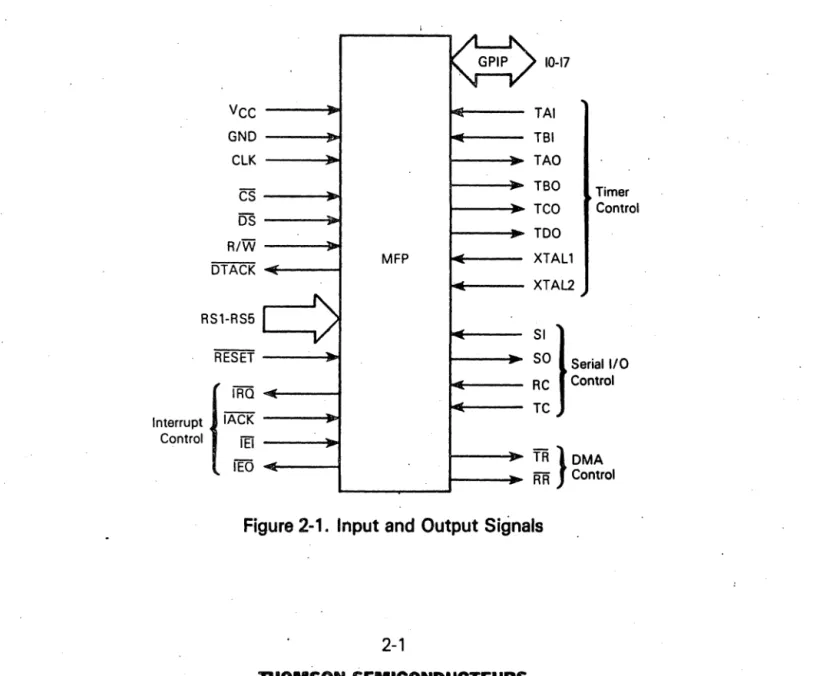
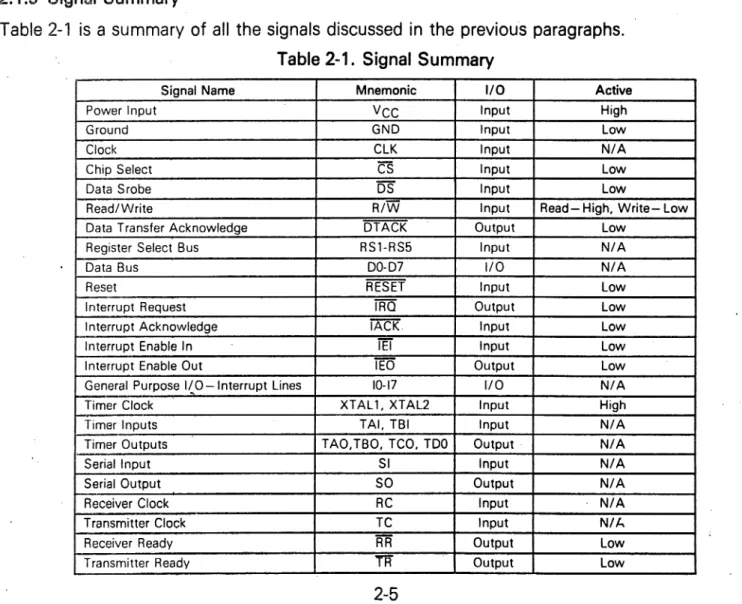
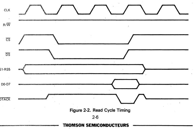
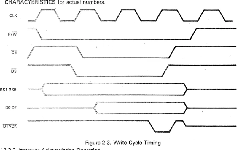
Specification
WRAP-1/68K
Revision C November 1985
ELTEC elektronik mainz
(C) 1985 ELTEC Elektronik GmbH, Kainz
ELTEC-68K-SYSTEK
Specification
WRAP-1/68K
Rev. C 11185
Page 2
This document contains copyrighted information. All rights
including those of translation, reprint, broadcasting,
photomechanical or similar reproduction and storage or
processing in computer systems, in whole or in part, are
reserved.
If single copies are made for professional
purposes with written approval of ELTEC, an aUowance will
have to be paid in accordance with para. 54.2 of Urh.G.
For details please contact ELTEC.
ELTEC reserves the right to modify without notice the
product described herein in keeping with state-of-the-art
technology at any time. Although this document has been
reviewed carefully ELTEC refuses any liability due to
misprints and detriments caused thereby.
This document is edited and printed by: ELTEC Elektronik
GmbH, Kainz
ELTEC elektronik mainz
SCOPE OF DELIVERY
The scope of delivery comprises:
Description
WRAP/68K
Operating Hanual
ELTEC-68K-SYSTBK
Specification
WRAP-1/68K
Rev. C
11/85Page 3
Order 10.
FE .68 05158
ELTEC elektronik mainz
lOT
E
ELTEC-68K-SYSTEX
Specification
WRAP-1/68K
Rev. C
11/85Page 4
If not otherwise specified, addresses are written in
hexadecimal notation and identified
bya leading dollar sign
("$").
James of voltage-level signals preceded
bya slash ("1")
indicate that this signal is active low.
James of edge-oontrolled signals preceded
bya slash
("1")ELTEC elektronik mainz
TABLE OF CONTENTS
1.0
General Description
2.0
VME-Eurocard specification
3.0
Address decoding
4.0
DTACK generation
4.1
Choosing local time delay signals for
VXEbus DTACK
5.0
Interrupt request and acknowledgement
5.1
Generating interrupts using the 68901
tnternal request sources
5.2
User generated interrupts
6.0
VXEbus control signals
7.0
Wire wrap connection areas
8.0
Using the digital wrap area
9.0
Example
ADEXE
Block diagram
Circuit diagrams
Part list
Jumper location diagram
IC location diagram
PAL equations
1K68901 data sheet
ELTEC-68K-SYSTEI
Specification
WRAP-1I68K
Rev. C 11/85
Page 5
Page
6
9
10
14
16
18
19
24
27
29
30
32
ELTEC elekt:!'cmHr
:mEdnz1.0 General Descript:ton
ELTEC-68K-SYSTEM
Specification
WRAP-1I68K
Rev. C 11/85 Page 6
Eltec 's e~{peri1ilEmtaJ. board \'lRAP-l/68K was created to free the design-eng:tneer frOJil V}'1Ebus-int'o1rface development and implementation of i:nterrupt-handling on hardware level. The VMEbus :is fully buffsTed and all signals are
on wire--vJrap"'p:tl1 j 8 \'itthi:o. specified ';·lrap-areas.
addreGs-decQ(:llel~ section creates '7 select-signals interfacing tls8r-·de:f:t1l('~able devices.
available The
for
Each device can cha:L!.l i.ts Qi'm "end o:f data transfer-signal" UDTACKJO to t:t,l.C: In:mbus DTAClt-sJgnal or one of the
timing-signals' ;~DLl~' to "DLlY' can h~ used i f there is no device depemieI\'I:. DTfiCIL-s:l.gnal available. The signals "DL1"
..• "DL8" iO:f?Jf3 'chI:: inIEbul;;'-s:lgni:tl lD'TACK
,"1
thin a timeinterval frOB (~i 118 to D(Y!) 118. Fo:-c !llore information see
chapter 3.0 .
Addressbus (sc1).J:K(un:l 2L1 bH) E\l1d dataous (32 bit) are fully buffered. B,2GDrlS8 a :32 blt c\atabuEl :ts irllplemented I the WRAP-1I68K cern.
n.t
m2';:o GEF~20-b(lsed EiYSte:mS and supportstrue long1:Jord C1,2!CE\ t:t!.lIcS:;:·;:):rs for flltBre use.
Address-ck:cod:tYl,j; :1.8 :EBll~? 2f.~ Mt standard-address-space incl uding i1ddT8C3S':-';:lOd:1.:Z:!.C'0:tE, Ii1i;)2,' 3 , L!: p 5. To select local devices, 512 byte or alte:rnat.ivly eit1k--byte address gaps are
divided :!.ntc H equal s·::!ct,1. ons, M byta respectivly 8k-byte long. By th1.8 vii).:; I it is possible to connect devices like serial- or pa:raU 081·- I/O thErt need s}llall address-gaps and ROM, EPROn or otll(~n3 tlfJ3.t D.8'3da large address-gap.
Card-Base-"addY'lC;ss- Bnd add:ress-modif:i,ar-selection is done by setting roti5lt:1. Ti,g·-j1(:~JI·-8;!;:i. t.ches.
For local USf:.2'E; clod~-8:tg:i.l;;;J.s are gell<:':rated in time
ELTEC elektronik mainz
ELTEC-68K-SYSTEI
Specification
WRAP-1/68K
Rev. C
11/85Page 7
To make \lse of the wide interrupt-facilities of VDbus
systems a 68901-device is on board the
WRAP-1/68K.
The
MK68901 is a multifunction pheriperal device with
interrupt-vector facilities. 16 Interrupt sources, 8 internal ones (
like timers, serial-I/O) and 8 external sources can trigger
an interrupt.
The possible interrupt service modes are :
poll~ng
status-bits reports the state of interrupt sources
. vectoring all 16 possible interrupt sources generate an
unique interrupt vector by changing the lower
4 bits of the programmed interrupt-vector-base,
The
IllC68901 includes an 8 bit parallel port with
programmable data direction or individual interrupt source
inputs with programmable edge selection.
A
f\lll-d~plexserial-port, supporting all
asynchro~us-formatsup to 62.5 kbps and synchronus up to
llfups .
v11th software-selectable sync-word, supports a
serial-communication-line. The transmit- and
receive-qhannels are independent and can be supplied with
separated clock-signals. For handshaking "receiver-
ready"-and "transmitter-ready"-signals are provided. Baud-rate
generatiQn can be done external or internal using the
on-chip timers.
4 timers with individually programmable prescaling and
independent clock-inputs give the ability of generating
ELTEC elektronik mainz
ELTEC-68K-SYSTEM
Specification
WRAP-1/68K
Rev. C
11/85
Page 8
They might also be used to generate a programmable baud-rate
for serial I/O-devices.
The
WRAP-1/68K board is prepared to install up to 7 user
definable devices with full interrupt vector support and
without additional decoding. The 1K68901 is the 8th device,
static mounted on the WRAP borad.
All signals to handle interrupt request and acknowledgement
and also DTACK generation for the 7 devices are prepared on
the WRAP-1/68K board.
The unused space on the right-half of the board is prepared
to hold digital-IC's and has a special hole-pattern with
support of Vcc and GID.
The front side of the WRAP-1/68K board is prepared for
insertion of one connector with D-Sub-layout ( from 9 to 36
pins, similar to RS232-connectors ) and one 96-pin
ELTEC elektronik mainz
2.0
VXE-Eurocard specification
Slave data transfer options
A24:D32
Interrupter options
anyone of
I(x)where
1<=
x
<=
7Enviro~ental
options
ELTEC-68K-SYSTEK
Specification
WRAP-l/68K
Rev. C 11/85
Page
9Operating temperature
Storage temperature
o
-70
degrees celsius
-55 -
85 degrees celcius
Maximum operating humidity: 85 per cent
Power options :
without user defined expansions
1.2
A max.
at +5VDC
ELTEC elekt:ronik mainz
3.0 Address--decoding on the WRAP-board
ELTEC-68K-SYSTEK
Specification
WRAP-1/68K
Rev. C
11/85
Page 10
Current VXEbus systems have typically 23 address-lines and
either short addressing mode (15 b:Lt, 64kByte) or standard
(23 bit, 16MByte). Address line A0 does not exist because
two signals
IDS0 and IDS1, the odd and even data-strobes,
are used to distinguish between e'i7en and odd byte locations.
To access peripherals via the VXEbuE), an address or
address-gap must be defined for cOmDlunication between master
and slave. Regard.ing the WRAP-bolirc1, the beginning of the
address-gap can be selected with hex-coded rotating
switches. This begin-address is called "card-base-address".
After setting the card-base-address, a global decision must
be done whether to use a 512-byte address-area divided into
8 separate 6'i-byte long parts or to use a 64k-byte area
divided into 8 8k-byte blocks.
The default card -base-address \'lhen delivered is $FE0000.
In case of 512 byte address-gap :
Jumper
"Ji"and "J2" in position
I
"81" to "84" select the base-address between
00 001{X and FF FFxx
ELTEC elektronik mainz
ELTEC-68K-SYSTEI
Specification
WRAP-1I68K
Rev. C
11/85Page 11
In case of 64k byte address-gap :
Jumper "Ji" and "J2" in position II
"83" and "S4" select the base-address between
00 xxxx and FF xxxx
"S5" assigns the address-modifier, see below
Table
1The following address-modifier-settings are possible and
valid for both address-gap-lengths :
AI5 AI(4 AI3 AJl2 AXi Al0
H H H H
d
d
Standard Access Supervisor
H H HL
d
d
Standard Access User
H L H H
d
d
Short 'Access Supervisor
HL
H Ld
d
Short Access User
L
L
H Hd
d
Extended Access Supervisor
L
L
HL
d
d
Extended Access User
Table 1
Address-modifler-setting
ELTEG elektronik mainz
ELTEG-68K-SYSTEI
Specification
WRAP-1/68K
Rev. G
11/85Page 12
The selected address-area is divided into 8 equal parts,
64-byte or 8k-byte long. For each part exists an associated
enable signal. These enable-signals are
IGSIFG and IGSl to
IGS?
IGSMFG enables the XK68901, IGSl to IGS? enable the
user definable devices.
Table 2 ( see next page ) shows the 8 enable-signals ICSMFG
and
IGSl to IGS? in relation with their activ address-areas
within the possible address gaps.
In addition, the
pin-numbers
an~connection areas on the WRAP board are
ELTEC elektronik mainz
ELTEC-6SK-SYSTEK
Signal
ICSJ[FC
ICS1
ICS2
ICSS
ICS4
ICS5
ICS6
ICS7
Table 2
512 byte gap
64k byte gap
BASE+$0 ...
BASE+$0 ...
BASEt$3F
BASE+$lFFF
BASE+$40
BASE+$2000
BASE+$7F
BASEt$SFFF
BASE+$S0
BASEtM000
BASEt$BF
BASE+$5FFF
BASE+$C0
BASE+$6000
BASE+$FF
BASE+$7FFF
BASE+$100
BASEt$S000
BASEt$lSF
BASEt$9FFF
BASEt$140
BASEt$A000
BASEt$17F
BASEt$BFFF
BASE+$lS0 .. BASE+$C000
BASEt$lBF
BASEt$EFFF
BASEt$lC0
·BASE+$E000
BASEt$lFF
BASEt$FFFF
ICSx
Specification
WRAP-1/6SK
Rev. C 11/S5
Page 13
IDTACKx
pin no.
pin no.
can. area can. area
"E"
"DTACK"
7
1
6
25
34
4
3
5
2 6
1
7
Chip select signals and valid address areas
"can. area" means connection area
Fan Out
101
loh
SmA
-400uA
SmA
-400uA
SmA
-400uA
SmA
-400uA
SmA
-400uA
SmA
-400uA
ELTEC elektlronik mainz
ELTEC-68K-SYSTEH
Specification
WRAP-1I68K
Rev. C 11185
Page 14
4.0 Data-Transfer-Acknowledge (DTACK) generation
IDTACK
is an VKEbus signal driven by slave-units to indicate
that the data was succsessfully received on a write cycle.
On a read cycle the slave-unit uses
IDTACK
to indicate that
the data has been read from memory and has been placed on
the data bus.
DTACK must
b1~generated for the 68901 and the 7 prepared
user-definable devices on the WRAP-1I68K board.
The 68901 pr()duces its own data transfer acknowledge signal.
This is named IDTACKMFC.
Two ways are possible for the
other 7 prepared local devices to generate the VMEbus
10TACK.
The first way is to use the DTACK-signal that is produced by
the user def:l.ned de"17ice.
In this case the device dependent
DTACK-signal has to be connected to one of the I/OTACK1" to
"/OTACK7"
pins on connection area "DTACK". The number of
the "/DTACKx
lP-pin must correspond to the number of tlie chip
select pin "/CSx" that was choosen to enable the device.
See table 3.
The second way is to use one of the time delay signals "OL2"
to "DL8", available on connection area "DL". One of these
bas to be connected to the "/DTACKx"--pin that corresponds to
the selected
cl:~ip-enable-signal( /CSx-signal ). See Table
3.
ELTEC elektronik mainz
used ICSx signal
ICS1
ICS2
ICS3
ICS4
ICS5
ICS6
ICS7
corresponding
IDTACKx signal
IDTACK1
IDTACK2
IDTACK3
IDTACK4
IDTACK5
IDTACK6
IDTACK7
ELTEC-68K-SYSTEM
Specification
WRAP-1/68K
Rev. C 11/85
Page 15
pin number
con.area "DTACK"
1
2 3 4 5 6 7
ELTEC elektronik mainz
ELTEC-68K-SYSTEX
Specification
WRAP-1I68K
Rev. C
11/85Page 16
4.1 Choosing local time-delay signals for VXEbus
IDTACK
To support devices that do not generate their own
IDTACK-signals, the local time-delay signals "DL2" to "DL8"
can be used on the connection area "DL". Table 4 shows the
selectable time intervalls. This time intervalls give the
minimal and maximal access time that a device needs to end
its internal. operation on read and write cycles.
The maximum access time of a user defined device must
reside within one of the 7 time intervalls listed in table
4.
from ns
to ns
con. area "DL"
DL2
0
81~2
DL3
80
205
3
DL4
205
33(~4
DL5
330
455
5
DL6
455
580
6
DL7
580
70E;
7DL8
705
830
8
Tahle 4
possible DTACK-Time-Delays
Example :
We assume that chip-select-signal
ICS3
enables a user
defined device. Its own DTACK-signal or an appropriate
"DLx"-signal must be connected to the "DTACK3" pin at the
"DTACK" connection area on the WRAP board to end the
V1Ebus-data-transfer.
If no on-chip-DTACK-signal is available, a local
ELTEC elektronik mainz
ELTEC-68K-SYSTEX
Specification
\7RAP-l/68K
Rev. C 11/85
Page
17exceeds the necessary time for the device to finish the
internal operations to read data or pass data onto its
data-bus-pins.
Comparing the m8xilnmn device access time against the time
values given in table 4 on the right column you have to use
the "DLx" signal \'lhose time value is equal or greater than
the maximum device access time.
Let us assume that the device needs a maximum of 260 ns
after the chip select signal goes activ to pass valid data
onto the local data-bus or to read the data available on the
local bus. Then "DLIl" must be chosen to be shure that the
maximum time of 260 ns is ahlays kept ready. "DL4" gives a
minimum time delay of 330 ns, v1hich is greater than the
maximum processing time of the chosen device.
The delay-time starts with the activ edge of the local /IOEN
(I/O-enable) signal. All address decoding processing times
are not involved and the chip-select-signals are valid
ELTEC elektronik mainz
ELTEC-68K-SYSTEX
Specification
WRAP-1I68K
Rev. C
11/85Page 18
5.0 VMEbus interrupt-request and interrupt-acknowledgement
On VXEbus systems, 7 interrupt-request-levels are available
with increasing priority from level 1 to level 7.
For interrupt-requesting the interrupt requester has to
drive one of the 7 VMEbus interrupt-request-lines with a
"low" signal.
After requesting an interrupt, a special interrupt
acknowledge cycle is initiated from the interrupt-handler,
usually a CPU-board. The activ IIACK-signal indicates the
beginning of the interrupt acknowledge cycle. All possible
interrupt-requesters in the actual system have to check
wheather
the~r:\lave requested an interrupt or not. To do
this check, the interrupt-handler passes the decoded
interrupt-request-level on address-lines Ai to A3 and the
interrupt-requesters compare the value against their own
request level. If there is a match and the daisy-chain
IIACKIN-signsll is
~lalid,the interru:pt-requester passes its
interrupt-vector-mnnber to start the
interrupt-service-routine.
ELTEC elektronik mainz
ELTEC-68K-SYSTEX
Specification
WRAP-1/68K
Rev. C
11/85Page 19
5.1 Generating interrupts using the MX68901 internal request
sources
For interrupt-requesting on the WRAP-1/68K-board, the
interrupt request level jumper "J3" must be set to the
appropriate request level you want to use. Position 1 of
jumper "J3" means levell, position 7 means level 7.
The same interrupt-level, jumpered at VMEbus IRQ level
jumper "J3" , has to be jumpered at the interrupt acknowledge
level jumper "J411.
Both jumpers can be moved simultanusely and must be plugged
at position-groupings listed in Table 5 for proper
operation.
VXEbus-IRQ-Level
( J3 )
VMEbus-IACK-Level
( J4 )
position
position
1
1
1
1
2 2 2 2
3
3
3
3
4
4
4
4
5
5
5 56
6
6
67 7 7 7
ELTF..; elektronik mainz ELTEC-68K-SYSTEK
Specification WRAP-l/68K Rev. C 11/85 Page 20
For proper interrupt-operation the XK6a901 must be
programmed in the right manner. See the following example programm. It shows you all necessary steps to do.
c
P /I
6
8 000 Ass e m b I e rSource File: b:demol.s
Revision 04.03 Page 1
1 2 3 4 5 6 7 8 9 10 11 12 13 14 15 16 17 18 19 20 21 22 23 24 25 26 27 28 29 30 31 32 33 34 35 36 37 38 39 40 41
1IIIIIIIIIIII!I!lllllllllllllllllllllllll
II general demo programm for interrupt
I requesting and interrupt service with
I the 68901
I
111111!11!!!I!IIIIIIIIIIIIIIIIIIIIIIIIIII
IWRAPBase equ $fe0000 Card Base Address
I
I this is the Card Base Address that must be I selected on the WRAP board
I
I address-modifier setting is standard supervisor mode
I that means $7 at hex-switch J15
I when using IRQ's supervisor mode must be used
I I
I 68901 Register Equates
I
GPIP equ $1 General Purose I/O AER equ $3 Activ Edge Register DDR equ $5 Data Diection Register
I
IERA equ $7 Interrupt Enable
IERB equ $9 II II
IPRA equ $b II Pending
IPRB equ $d
ISRA equ $f ISRB equ $11
lIRA
equ $13 IIRB equ $15! II II II II II II In-Service II Mask II
Register A
B A B A B A B
VR equ $17 Interrupt Vector Register
I
TACR equ $19 Timer A Control Register
TBCR equ $1b II B II II
TCDCR equ S1d II C and D Control Register
rADR equ $1f II A Data Register
TBDR equ $21 II B II II
TCDR equ $23 II C II II
42 43 44 45 46 47 48 49 50 51 52 53 54 55 56 57 58 59 60 61 62 63 64 65
ELTEC elektronik mainz
66 00000000 2C7C00FE0000 67
68 69 70
71
72 00000006 '703E '73 00000008 4E42 74 0000000A 224F
75 0000000C 2E7C00027000 '76 7'7 '78 79 80 81
82 00000012 203C00000080 83 00000018 1D40001'7 84 0000001C E580 85 0000001E 2040 86
X
ELTEC-68K-SYSTEM
Specification WRAP-1I68K Rev. C 11/85 Page 21
I
special equatesI
WVEC equ ($200»2) 68901 base vector number
TaPrio equ ($dI4) internal Interrupt priority Timer A TbPrio equ (814)" " " II B
I
TIRQen equ $21 value for Timer interrupt enable
IRQdis equ $00 value to disable or mask all interrupts ResetT equ $10 value to reset a timer
X
TIMaCONST equ $40 Timer A Data register start value TUlbCOBST equ $20" B II II II II
I
TaJlode equ $6 Tblode equ $'7
I
IIXXXIIXXIXIIXIIIXIIIIIIXIXIIIIIIIIIIIIIIIIIII
X
X lilT setup's the interrupt service routines
I and interrupt vector number
X
IXXXXXIXXXXXXXIXXIIXXIXXIIXIIIIIIIIIIIIIIIIIII
IINIT move.l #fffiAPBase,a6 pointer to WRAP and 68901
I
I s\"li tch to supervisor mode
I this is done here using an system command
I of the CP/M-68K operating system
X
moveq #$3e,d0 system command code trap #2
move.l a'7,a1 save a7
move.l #$2'7000,a7 setup new stack start addresss
I I
I WVEC contains the interrupt vector number you want to USE I This number must be multiplied by 4 ( shift 2 times left
I to get the right entry into the interrupt address table
X
move.l #WVEC,d0 get interrupt vector number
move.b d0,VR(a6) write vector number into VR-register asl.l 92,d0 shift two times left
move.l d0,a0 setup pointer to interrupt address table
87 88 89 90 91 92 93 94 95 96 97 98
ELTF~ elektronik mainz
99 00000020 217C0000005A0034 100 00000028 217C000000880020 101 102 103 104 105 106 107 108 109 110
111 00000030 ID7C0040001F 112 00000036 ID7C00200021
113
114 0000003C ID7C00060019 115 00000042 ID7C0007001B
116
117 00000048 ID7C00210013
118
119 00000048 ID7C00210007 120
121 122 123 124
125 00000054 4871 126 00000056 4871 127 00000058 60FA 128
ELTEC-68K-SY8TEM
Specification WRAP-1/68K Rev. C 11/85
Page 22
1111111111111111111111111111111111111111111111111111111111)
I
I The actual interrupt service routines are setup in
I the interrupt address table.
I The con tense of Register a0 is the main pointer to this
I area.
I Because the 68901 varies his interrupt vector number in
I relation to the requesting event, (a0) is modified by thE
I interrupt priority level.
I
IIIIIIIIIllll~IIIIIIIIIIIIIIIIIIIIIIIIIIIIIIIIIIIIIIIIXlIIi I
move.l ITaIRQ,TaPrio(a0) setup IR-service-routine Timer A move. 1 #Tb I RQ , TbPri 0 ( a0 ) " " " " "B
I I
IIIIIIIIIIIIIIIIIIIIIIIIIIIIIIIIIIIIIIIIIIIIIIIIIIIIIII
II TimTest starts the two Timers A and B for free running
I and interrupt requesting on 1 to 0 transition in their
I data registers
I
111111111111111111111111111111111111111111111111111111II
I
TimTest move.b #TIMaCOIST,TADR(a6) setup Timer A Data reg move.b ITIKbCOBST,TBDR(a6) setup Timer B Data Register
I
move.b ITaMode,TACR(a6) setup Timer A operation mode move. b ITblode, TBCR (a6) " " B " "
I
move.b ITIRQen,IJlRA(a6) unmask Timer A, B interrupts
I
move.b ITIRQen , IERA(a6) enable Timer A, B interrupts
I I
I from now on, only interrupt activity will take place
I I
Loop nop nop bra Loop
ELTEC elektronik mainz ELTEC-68K-SYSTEX
129
130 0000005A 48E70002 131 (b000005E 2C7C00FE(b00(b 132 0000@064 lD7C00100019 133 0000006A lD7C00000013 134 101010001070 lD7C004(b001F 135 010000076 1D7C00060(b19
136 (b000007C 1D7C0(b2101013 137 101010001082 ~CDF4000
138 0101000086 ~E73
139 140 141
142 00000088 ~8E70002
143 0000008C 2C7C01OFE0000 144 1000100092 lD7C0010001B 145 00000@98 1D7C00000015 146 0000009E 1D7C00200021
147 000(b00A4 lD7C0007001B 148 0010000AA lD7C00210015 149 000000B0 4CDlJ40~)0
150 000000B4 4E73
151 000000BG
S J ill b 0 1 T n b 1 e
Alln
rm:!Il
IPRA
ISRB TADTI TCDn TaIRQ TblIoQ·:)URAPBase
GPIP lIIRB IRQdis ResetT TBDll Ti1-1bCOlTS TaPrio TimTest00000003 il.BS
(i)1?;000f<;09 ABS 0001lJ00fiiB ADS 00000011 ADS fl)00000JJ! ABS
00000023 ADS
0000005Ji. TEXT 0000(])(J)I!J7
ABE
00FE0000 ADS
019000001 ADS 00000015 £lBS 00([;00t])(!)0 ABS
0(j)(j)0~)010
ADS
00000021 liBS 00({)Q)(I)020 ABS
00000!i)311 ABS
000tD0030 TEXT DDR
Specification WRAP-1/68K Rev. C 11/85 Page 23
IJ.
TaIRQ movem.l a6,-(a7) move.l nURAPBase,a6
X
move.b #ResetT,TACR(a6) Timer A RESET
move.b UIRQdis,IMRA(a6) mask interrupt Timer
A
move.b UTIMaCOIST,TADR(a6) set new start value move.b #TaHode,TACR(a6) setup Timer A operation mode move.b #TIRQen,IXRA(a6) unmask interrupt Timer A movem.l (a7)+,a6
rte
X Timer B interrupt service routine
K
TbIRQ movem.l a6,-(a7) move.l a~TRAPBase,a6
move.b DResetT,TBCR(a6) move.b CIRQdis,IKRB(a6) move.b UTIMbCONST,TBDR(a6) move.b CTbUode,TBCR(a6) move.b #TIRQen,IXRB(a6) movem.l (a7)+,a6
rte end
HInA
IPRB
LoopTBCR
THlaCOTIS TruIode TbPrio t7VEC(ll0@00005 ABS G0000013 ABS 0000000D ABS Q)0000054 TBXT
0000001B ABS 00000040 ABS
00000006 ABS 00000020 ABS 00000080 ABS
lERA
0({)000007 mIT (j)(j)(j)0001lJ0ISHA
0000000FTACH 00000019
TCDeR 0000001D
TIRQen 00000021
TbIRQ (})0000088
EI'.EC elektronik mainz
5.2 User generated interrupts
ELTEC-68K-SYSTEK
Specification WRAP-1/68K Rev. C 11185
Page 24
For WRAP users, who want to service their devices with vectored interrupt routines, the secound example program shows how the 68901 has to be initialized.
One pin of the a-bit I/O-port is configured as an input. The actic edge to trigger an interrupt-request is a "1" to "0" level transition at this pin. See the following program for details.
C P j I 6 8 0 0 0 A 8 8 e m b 1 e r Source File: b:demo2.s
Revision 04.03
I demo programm for interrupt
Page 1
1 2 3 4 5 6 7 8 9
I requesting and interrupt service with
10 11 12 13 14 15 16 17 18 19 20 21 22 23 24 25 26 27 28 29 30
I interrupt requests on the 68901 parallel
X
portI 1
X
Init and setup of the 68901X
to request vectored interrupts when1 receiving an activ negativ edge on lone of the 8 input pin's
I
X
YRAPBase equ $fe0000 Wrap Base Address X
X Register Equates
X
GPIP equ $1 General Purose I/O AER equ $3 Activ Edge Register DDR equ $5 Data Diection Register
1
IERA equ $7 Interrupt Enable IERB equ $ 9 " "
IPRA equ $b " Pending
IPRB equ $d " "
ISRA equ $f " In-Service
ISRB equ $11 InA equ $13 IKRB equ $15
I
"
""
"
Xask "Register A
"
B
"
A
"
B
"
A
"
B
" A
"
B
31 32 33 34 35 36 37 38 39 40 41 42
ELTEC elektronik mainz
43 00000000 2C7C00FE0000 44
45 46 47 48
49 00000006 203C00000080 50 0000000C 1D400017 51 00000010 E580 52 00000012 2040 53 54 ~~ 56 57 58 59 60 61 62 63 64 65
66 00000014 217C0000003A0000 67 68 69 70 71 72 73 74 75 76
77 0000001C 1D7C00000005 78 00000022 1D7C00000003 79
80 00000028 1D7C00010015 81 0000002E 1D7C00010009 82
83 00000034 4E71 84 00000036 4E71 85 00000038 60FA 86
I
I special equates
I
ELTEC-68K-SYSTEK
Specification WRAP-1/68K Rev. C 11/85 Page 25
WVEC equ ($200»2) 68901 base vector number
I
PinIRQb equ $01 GPI0 equ (014)
I I
1 lilT setup's the interrupt service routines
I and interrupt vector number
I
lilT move. 1 IWRAPBase,a6 pointer to WRAP and 68901
1
1 WVEC contains the interrupt vector number you want to uS( 1 This number must be multiplied by 4 ( shift 2 times left
1 to get the right entry into the interrupt address table
1
move.l #WVEC,d0 get interrupt vector number
move.b d0,VR(a6) write vector number into VR-register asl.1 #2,d0 shift two times left
move.1 d0,a0 setup pointer to interrupt address table
1
1111111I111I1111I1111111111I111111111111111111111111111111)
1
I Jow the actual interrupt service routines are setup in
I the interrupt address table.
I The contense of Register a0 is the main pointer to this
I area.
I Because the 68901 varies his interrupt vector number in
I relation to the requesting event, (a0) is modified by th.
I internal interrupt priority level.
I
I111111111111111111111111I111111111111111111111111111111111
I
move.l #IRQ0,GPI0(a0) setup IR-service-routine for Input
I I
111I1I111111111111111111111111111111111111111111111111l
I .
I PinlRQ initializes the 68901 for interrupt
I requesting when an 1 to 0 transition occurs at the
I I/O-pin 0
I
1111III1IIIII1III111I11I1I1I11111111111111111111111111II
1
PinIRQ move.b #$0,DDR(a6) all I/O-Lines are Inputs move.b #$0,AER(a6) activ transition is 1 to 0
1
move.b IPinIRQb,IIRB(a6) unmask interrupt for I/O-pin 0
move.b IPinIRQb,IERB(a6) enable interrupt on I/O-pin 0 1
Loop nap nap bra Loop
1
ELTiC elektronik mainz ELTEC-68K-SYSTEK 87 88 89 90 91 92 93 94 95 96 97 98 99 100
101 0000003A 4E73 102 0000003C
S y mba 1 Tab 1 e AER
I ERA
UnT ISRA PinIRQb GPI0 IJIRA IPRB Loop WRAPBase
00000003 AOO 00000007 ABS
0000000(~ TEXT 0000000F ABS 00000001 ABS
00000000 ABS
00000013 ABS 0000000D ABS
0000003'i TEXT 00FE0000 ABS
DDR IERB IPRA ISRB VR Specification WRAP-l/68K Rev. C 11/85 Page 26
111111111111111111111111111111 I
I Interrupt service routine
I
IIIIIII!!II!!IIIIIIIIIIII!III! I
I reset the external event clear the interrupt
I pending- and interrupt in-service bit if no
I automatic end of interrupt mode is used.
I For "end of interrupt modes" see page 6 of
I the 68901 data sheet.
I These program steps are not shown in this demo
I program.
!
IRQ0 rte end
00000005 ABS 00000009 ABS 0000000B ABS 00000011 ABS 00000017 ABS
ELTEC elektronik mainz
ELTEC-68K-SYSTEI
Specification
WRAP-1/68K
Rev. C
11/85Page 27
6.0 VMEbus control and information signals
All VlEbus control signals that give the state of valid or
invalid address- and data-lines, that mark read or write
cycles and that determine the data transfer-mode ( 8bit,
16bit, 32bit ) are buffered and available to the user at
connection area
"G".
lAS
address strobe, if low the address-lines Ai to A23
keep an valid address
Ioh
=
-15mA,
101
=
24mA
11)80
odd data byte strobe, Ioh
=
-15mA,
101
=
24mA
11)81even data byte strobe, Ioh
=
-15mA, 101
=
24mA
ILWORD
longword select, loh
=
-15mA, 101
=
24mA
IWRITB
if low, an write cycle is indicated·, Ioh
=
-15mA, 101
=
24mA
ISYSRESET system reset, activ low signal to force all hardware
devices to their initialisation state.
ISYSCLOCK
S/2
to
S/256
loh
=
-15mA, 101
=
24mA
Bain clock signal ( 161Hz ) and divisors
inpowers of
2ELTEC elektronik mainz
VKEbus information signals
ELTEC-68K-SYSTEX
Specification
WRAP-1I68K
Rev. C 11185
Page 28
Al. .A15
D0 •• D32ELTEC elektronik mainz
7.0 Wire wrap connection areas
ELTEC-68K-SYSTEX
Specification
WRAP-1/68K
Rev. C
11/85
Page 29
10 wrap-pin connection areas are marked on the WRAP board.
The following chapter gives an overview of the purposes of
this areas.
Connection
area
"A"
all signals of the 68901 to interface the serial port,
see 68901 data sheet
"B"
all signals for interfacing the parallel port and the timer
signals of the 68901, see 68901 data sheet
"CII
interrupt enable daisy chain signals of 68901,
see 68901 data sheet
"D"
data-bus lines D0 to D31
"E"
local chip select signals
ICS1 to ICS?
"F"
address-bus A1 to A15
"G"
VXEbus control signals, see chapter 6.0
"H"
clock signals, time intervall from 0.0625 us to 16us
special areas
ELTEC elektronik mainz
8.0 Usage of the digital wrap area
ELTEC-68K-SYSTEK
Specification
WRAP-l/68K
Rev. C 11/85
Page 30
The digital hole-pattern is assigned to fit with all
integrated circuit pin layouts starting with 4
I0.1 inch
width to a 60 pin dual-in-line-package with 10
I0.1 inch
width.
A symetric grouping in regard of the +5V and
GID
lines can
be used for all pin-layouts with 4
I0.1 inch width. See
figure 1.
For IS's with greater widths than these ones, an
unsymetrical grouping has to be used. See figure 2 and 3.
4)(
0,1 INCH
INTERVAllS
ELTEC elektronik mainz
ELTEC-68K-SYSTEX
Specification
WRAP-1I68K
Rev. C 11185Page 31
"
.
=t-~+l==h=~~~
. .::_.
-7
~0,1
INCH
I NTE RVALl 5
Figure
2
10
X·0,1 INCH
INTERVALlS
ELTEC elektronik mainz
9.0 Example
ELTEC-68K-SYSTEK
Specification
\mAP-1I68K
Rev. C
11/85Page 32
A little problem should be solved as an example how to use
the WRAP-1/68K-Board. An MB8128 static memory device
should be interfaced to the VMEbus.
The 8128 contains an 2K
1 8 organisation and is addressable on the WRAP-borad using
the 8k-byte address-gap mode. That means jumper "Jl" and
jumper "J2" have to be plugged at position II.
Addres-lines Al to All from the VKEbus ( connection area
"F", pin 1 to pin 11 ) have to be wrapped to the address-bus
pins A0 to A10 at the 8128 device.
We use chip select signal
ICSl ( connection area "E" ) to
enable the device and the IWE ( connection area "G" ) line
to determine the data transfer direction. The 8
data-bus-lines of the device are connected to the VMEbus
data-bus-lines D0 to D7 ( connection area "D"). Hence it
follows that all odd byte locations mean the memory-cells of
the 8128 device that can be read and written. All even byte
locations are on the VlEbus termination voltage level and a
cpu read cycle will read
"ff".
The 8128 device has a maximum access time of 140ns for read
and write cycles. Regarding table 4 of this manual, we
choose "DL3" to form the
IDTACK signal for access cycles on
the 8128. The maximum access time of 140ns is within the
time intervall "DL3" that ranges from 80ns to 205ns
The simple way to use only
IC81 for chip enable results in
an reflected image of the memory-contents in the 8k-byte
address gap.
ELTEC elektronik mainz
ELTEC-68K-SYSTEK
Specification
WRAP-1/68K
Rev. C 11/85
Page 33
Signal ICS1 was chosen to enable the memory device. Hence
it follows that the MEMORY_BASE_ADDRESS is the
ELTEC elektronik mainz
ADDRESS - BUS
F
A11)
,,.'
,--·A 9
9-A 8
8-.A 7 A7 1
7- :A 6 A6 2
6
,A 5 A~ 3
5
A 4 A~ 4
4
A 3 A 3 5
3
2 A 2 A 2 6
1 A 1 A 1 7
r...;.. AJl B
r-lL
07 Jl0 97"
06
o
1 106"
~5 02 11
5
0_4 12
4 L
,
3'"
0302
2
01 1
0 .-0.0
DATA -BUS
..L
7 ICS1
---r-!L
,
IWRITE---ELTEC-68K-SYSTEI
Specification
WRAP-1I68K
Rev. C 11/85Page 34
•
23 A8
l22.
u
WE 21 IWRITE
20
---OE
~1f)
19
CE 18 ICS1
17 07
16 06
15 05
~ 04
13 03
Figure 4: example circuit-diagram
"
ELTEC elektronik mainz
Annexe
~
INTERRUPT
~ADDRESS
LOGIC
DECODING
V-and
~"
CHIP-SELECT
ADDR:-BUS
+AM)
GENERATION
VME-
BUS
BUS
TRANSFER
K
ALOGIC
P1
ADDRESS-BUS
ADDR:-BUS
)
v
BUFFER
"
CONTR.- BUS .)
CONTROL-BUS
BUFFER
',:VME-BUS
DATA-"P2
DATA - BUS)
BUS
BUFFER
..
)
-.
vMULTI
FUNCTION
-:>
DEVICE
)
v...
...
~
....)
--y ")
--v ""-/
")
--v 0 0 0 0 0 0 0 0 0 0 0 0 0 0 0 Q 0 08 BIT
PARALLEL PORT
or
8
INTERRUPT
EVENT INPUTS
SERIAL PORT
and
TIMER
ADDRESS-BUS
USER CHIP-SELECTS
and
TIMING
VME-BUS
CONTROL-and
TIMI NG -SIGNALS
~ IIRQ1
~ IIRQ2
111@ IIRQ 3
I1llli
/IRQ4~ IIRQ5
~ IIR06
~ IlRO 7
3/
17U 23 .1
o ~~-~----~~~
o ...
OATA- BUS 2 ...
,
o " 0 - - -....
o ~o---....
o n.u---.... o ~o---....
o "0---'
J3
IRQ - LEVEL - JUMPER
U
23.
'-+
1.11 c IBERR 5 «1-15::...----,1.,9 1.220 t-~/=IA~C~K=O=U~T ____ _t_---~13,.-3.4AOOR.- BUS
1.16 a 10TACK
II N 14 IILACK 1B IOEN 12
I OBUFENH 17
I OSUFEN 1 10
I OBUFEN Ol 15
IILACK
U
23.3
4 «J-16 _ _ 1--15
16
NC
OIR 1 •
•
U
23
G
19 I•
INTERRUPT ACKNOWLEGOE LEVEL - JUMPER
,
G2B 5
J4 Y f 1-'1....:...4 - - - 0 0
-Y 2 13 ~ 0---4
Y 3 12 ~ 0---4
Y 4 1-1 0---4
U 20
Y5 10 0---4Y6 t-=9=---o
Y 7 J-!7---O
C 3 A3 B 2 A2 A t-'1'---'-'AC-:.1 __ ----..
"-G 2 A t-4-'----'-I-'-'A-=.S_~
5 Q +
R1 CK
0.~2'----
____ 4 -_ _~I~
____
-+ ____~/I~N~T....:...R=---~3~2
PRE R5 3
~
7
U6
A1
4
r1....:...7 __
~X~T~A=L~1
____~I~~~A
18 XTAL2 L ..02'.-=9=---'5::..:1=---_____ +-'. -0 3
2
A2 3
U23.6
A
13
A3
~O ~~
!~ ~I
1-'-7 ____ T.:....:C=----____ -+--i)~ 0 .
A4 5
A5 6
v
G1t-=6=---~II~N~ __ +-~r-__ - . __ ~20
o
5 12 0 Q 1-"9 __ --,~~ ~= ~~
U 21
U
22
5 II LM
3 IIACKIN 8 ILWORO 4 lIND 6 IICHECK 7 IDS 1 1 ICAROBASE
2 I OSOl 9 IIACK 11 I A 1
1 J OTACKMFC 2 I CSMFC
3 OTACK 1
4 I CS 1
5 OTACK 2 6 I CS2 7 . DTACK 3 8 I CS3 9 OTACK 4 11 ICS4
12 OTACK 5
13 I CS 5
14 OTACK6
17 I CS 6 18 OTACK7 19 I CS 7
U5
U5
r----...:3'-1CK 11 CK
CLR DOl 37
I 4'
!
I
_ !
5I ~ 6
- !
CLR PRE
1 4
+
5-:-2
DL
['_1
OL1 .; - i OL23 o-t--=0..::;.L.::::....3 _ ...
4 i OL4
5" DL5" 6 ! OL6 7"" OL7
i
8!
OLBL.--.J
PRE
v
R4
01 38
02 39
03 40
04 41
05 42
06 43
07 44
IDS W 47 ISYSRES 21
I CSMFC 48
I WRITE 1 57-4 35
II LACK 45 10TACKMFC
46
I I EI 34
nEO 33
U
1
11 36
F2~2_~I~QJ
_ _-+I~·~B
~~
U : -
~I
!-='---=-~---+--o_ 4 .
r2=6_~I~4 _ _ ~~5 27 15
j. 6
~2=8_~I~6 _ _ ~~7 ~2=9_~I 7-'---1!--o_ 8 .
13 TAO ,-,9
14 TBO
" ,-,10.
~5 TCO
-11
16 TOO
19 TAl ! ... 12
~---=-~---+--o13 .
20 TBI L....o.
~
+
~
___________
-_~
______________
~r~,~0C
I ~
21
L" .
.J
DIN - Nr .:. ~ en Pos st.-Z
I
BenennungI
Werkstoff~ ~ ~ Werkstoff / Gertitetype: PAGE 1 of 5
WRAP -
1.
/68 K
~ 2'~ ~---l---+--+----I
CII g'
j
Zlst Anderung Oat\... , ,_".0 :J ~
ill
~~~b
....,(..:::;.~~;l...::...~;...t'f-+:-....,-;Nam~I>--·--t ~§!NG
DIAGRAM 1
:::;z~lKI
E
I
3 42.
DATA - BUS
-J 1 I P1
D 0 11
1.1 a I---=--=---~
1. 2 a 1--_ _ --=O~1!__ _ _ _ _ _ _!1.!:..12
02 13
1. 3 al----....!:!....!=---~
03 14
1.L.al----~~---...:..:!..j
0[' 15
1. 5al---=:....::=---~
05 16
1.6 al----~~---~
1. 7 al--_ _ ....!:0~6:!..._. _ _ _ _ _ ~1'_47 ~-~0~7~---~18~
08 18
1.1 cl---=--~---__=__t
09 17
1.2 cl----~=---__!..!...j
010 16
1.3 cl----~~---~
011 15
1.4 cl----~~---___=..=..j
012 14
1. 5 cl----~:..!::...---__.:..::..t
013 13
1.6cl----~~---~
014 12
,. 7cl----~=---...:...=..g
015 11
1. 8c·I----...!::..-~---.:...:....&
J2/P2
016 11
2.14.ti---=....:...::...---.:...., 2.15bll---!D==-.1:..!.7---..:.!:.I12 2.16b,I--_ _ -.!:0::....;1:..,:::8 _ _ _ _ _ _ 1-=-13
2.17bl---=0::...,:1....::.9---1:..:!.14 2.1Bbl--_ _ -=0~2~0:...-_ _ _ _ _ 1~5
2.19bl---=0~2:....:.1---1~6
022 17
2.2Jti----~~---=-~
221~---=0~23==---~1~8
024 11
2.23b1---~~---=-.!....f
025 12
2.24ti----~-==-=---=-~
026 13
2.251b1---!:::::~---=-,
027 14
2.26,bI---!:::::..=..:...---....:.,
02B 15
2.27'bI---!:::::~---=-!:..I
228li-_ _ -..!:!.0=.:29:!...-.-_ _ _ _ _ ....:.16~ 2~b~---=0~3~0---~1~7
031 18
2.3011:i---!:::::..::...:....---.:.,
U13
19 19U 14
U15
19 19U16
9 B 7 6 5 4 3 2 2 3 4 5 6 7 8 9 9 8 7 6 5 4 3 2 9 8 7 6 5 4 3 2 DIDo
102 03 04 05 06 07
I OBUFEN ID
IWRITE
10BU FEN 1
08 09 010 011 012 013 014 015
016 /
017 /
018 /
019 ./
020 ./
021 /
022 ~
023
IWRITE /
I OBUFEN H ~
024
025 ./
026 027
028
029 ./
030 ./
031
DATA - BUS
o
____ ---..::o::....=:rD:...----+f-· ~
,---=~~;=---+-_o
;
I
,----=O~3
_ _-+!--o~
4 .04
I
o
5!~!
o
6~
7 8\o
7T
~I ,--~----+--o
,----=:~~1~~~
---1!I---O=
~~I
o
11 ~"
'----'=~:..:...~ ~!.-
_ _ _11--O=;~
I
DATA - BUS'---=:0:....:.;18~ _ _+_-o 19'
"
019~21D1
'--~0:..!::2~0 --I--O~ 21
021 .
2
23
21'
022
023
!
-24.024 ! --25
I
I\. '---!:~--+--_o-o26 025 ,
o
26~271
027
'---=~--+-_o_v 28
1\..'--~0~2B:!...---+-_ov29·
029 :
rJ
'---=0~3~0
_ _+--v_o~~
031 . 1321
L.~
~ ~ ~ Pas.
st.-z.1
BenennungI
Werkstotf' DIN - Nr. - Nr.~ E j~~~~----~--~~~~---~~~~~--~~~~--~~~~~~
... m • Werkstoff / GeratetypePAGE 2 of 5
~ ~~
a 1 - 32 D.-BUS~.2.~~
WRAP
-1.
/68K
~
5
~ Zust. Arderung10c:M1
I_'""
o
~ ~~Iab 1~~~~V
- .BWi'RiNG DIAGRAM
2
~:_:_~..::.-..::.8~...:...·K.:....:/~.!-/...:!I!3~9:....-:4:...!:!2=---I
'·4 ADDRE55 BU5 AND CONTROL BU5
.- , -
-~
,
..gRN:
J 1 I P 1 + 2 3 1
51
An 2 18 511
A9 4 S I l. C 2 A7 4 16 52
1.29
-
20
1.28c A 10 6 7 3 4 C 5 A8 6 14 53
l27c A 11 B
U2
9 h S...
• 8U7
~A 12 11 12 1 1 A 13 I 11 9 513
1.26c
A13 13 14 t. 2 C 2 A14 13 7 514
."
1. 25
..
(3
"
1.24c A 14 15 16
-
3 4 C 5v
A15 15 5 51'5"-123c A15 17 18
...
6 S 17 3 +I
'
-1
1952
119 1 II +--0
QRN2
J211
1.22c A16 11 18 1 1
53
1.21 c A17 15 16 4 2
0
C 2..
1.20c A 18 13 14 3 4 C 5
1.19 c A19 11
U3
12 6 B--1.18c A 20 2 3
..
1 11.17 c A21 4 5 4 2 C 2
1.1oc A 22 6 7 3 4
(2)
C 5 51113 1 A 15 C5MFCA 23 8 9 6 B 52/14 2 B 14 C51 ICS 1
r·
1.15c ""
_
.. 53/15 3 13 C52'"
IC52 !C
U 8
1 19
54
12 C53"\,
IC53
1 C54
"'
IC54!
~.-
IOEN6 G1 10 CS 5 -..:;;: /C5 5
/
"'
5 G2B 9 C56
-
/C56{ RN3
"'
61
4 G2A 7 C57 IC57 ~J 1
'"'"
.EL.
2 3 .1- CARDBASE
~
~4 5
!
;---L.J
L..-.
AM2 6 7 I
!
1 155
118
1.19b AM3 15
U4
16 4 2 C 2I?~
1.230 AMI.. 8 9
-
3 40
C :,114c AM 5 13 14 6 8
U23.5
/IACK 11 12 +
...
1.20
1.1 Bo / A5 17 1B I I
1 19
.... / CARDBASE
,
~ ~ ~rP~O_S-FS_t-~Z_I
____
- r __ ~BM~enT.n~U~ng~~~~~__
~lw~e~~~s~to~ff~__
~~.~D~IN~-~~~. ___ ~lz~e~iC~m~I~~~.-N~r~.E
~
Werkstoff / GerOtetype PAG E 3 of 5e a.::re c
§
2E
1--+---~---4--1
WRAP
-1.
/68K
~ §lP'z~~~tq.qAn;~d-«~~u~~n-\gl:~~~-~~~-~~'-~'.-'~-~~~~~~
__
~~~~~----~~~~~~~~~~--J
&
.21... Manstat Datum NcIIN Benennung: Zchng. - Nr. :i
~
i -/.
-17. 12.,'I
.~
WIRING DIAGRAM
·3
.
68 K
lEI 3942
1·3 ADDRESS BUS AND CONTROL BUS
-
,
-
--
'"
J 1 I P 1
1.18 a I AS 11 9 lAS
1.300 A 1 2 18 A1
1290 .A2 4 16 A2
U9
1280 A3 6 14 A3
1. 70 A4 8 2 A4 /
1.260 A5 17 3 A5
1.250 A6 15 5 A6
1.240 A7 13 7 A7 /
'\. DL1
1 19
'"
DL2
..i---
r... DL3r... DL4
I\. DL5 I\. DL6
i\- DL7
I\. DL8
1.30c AS 17 3 A8
1.29c A9 15 5 A9 /
1.28c A10 13 7 A10 /
U10
1.27c A 11 11 9 A 11
1.26c A 12 2 1B A12 /
1.25c A 13 4 16 A13 /
1.24c A14 6 14 A 14 /
1.23c A15 8 12 A 15 /
\.. S-:'-2
1 19 \.. S-:-4
'\. S..;-8
.-
--i\- S ~16
I\. S ..;- 32 I\. S +64 I\. S.;-12B
S..;- 256
1.12c ISYSRESET 2 18 ISYSRESET
1.100 SYSCLOCK 15 5 SYSCLOCK ....
J OS QJ 4 16 IDS QJ
1.130
U 11
1.120 IDS 1 11 9 IDS1
1.140 IWRITE 8 12 IWRITE /
1.210 JlACKIN 17 3 IIACKIN
1.200 IIACK 13 7 flACK /
1.13c f LWORD 6 14 fLWORD
1 19
....
.1..
"-+ +
1 2
3 OA 4 5 QB
QC
U18
610 QD 9 IOEN
QE CLR
11 12 OF 13 QG QH CK 8 B MHz 3 4 5
6
U 12
11 13
1(])
9 1 SYSCLOCK
8
2 12
.-
.1-I
...
Pos. St.-Z.'\ -... BenefYlun A1 A2 A3 A4 A5 A6
'"
A7 ASA9 A 10 A 11 A 12 A 13 A 14 A 15 lAS JDSQ) IDS1 IWRITE
I SYSRESET JlACK IIACKIN '" f LWORD
SYSCLOCK S.;..2 S74 S..;-8 S .;-16 S .;..32 S .;- 64 S .;..128 S~256
I.'
-vn
~
i -."
1 '"
! '"
~ -... ! : -v n ! -... n -... ! '" -...
1 v
~F
2. 3 4 5 6· 78 ADDRESS-BUS 9' 1QJ 11 12' 13 14
L~
~ 1,?'
1"--n
~G
-v 2,
3
~ ~
~.()
! '"
i ...,
! '"
L~
r---~ , . "
....
I -... n
T -v
- ~
-v -r ....
-v
n
_.
4 VME - BUS-SIGNALS 5'
~l
8'.J
~H
8·7 CLOCK - SIGNALS
6 5, 4 3 2 .-J GI
t - _ t -_ _ _ _ -+_-+_-tWerkstoff / Geratetype:
WRAP - 1. /68 K-'
ELTEC
Zust And.run
BWlRlN
G DIAGRAM
4
Zchng.-~K
I EI 3942
. ErtGtz fUrManstob Datum
-~+5V
J 1 I P 1
+5V .5V + 5V
T
C101
.~
~~.12V
~ + 12V
,
I
C2JJ
T
~:l_12V
[DIQ) -12V
f
I
C3I
J
I
GND 'lGND
+ 5V S
~~+_5V~S~TA~N~DB~Y
________________________________~t~~~~:JI
.!. ~ ~ Pos.
st.-zT
s.nennungI
Werkstotf DIN - Nr.I
Zeichnungs - Nr.!II .- :)
> E 01 . Wer kstotf / Geratet~ PAGE 5 of 5
ELTEC
-0 '-'E
C E.c::.
WRAP -
1.
168K
::) !II !II 01 C
..Q C ~
MaOstab
&Ei
Datum .. NorM a.n.nnUng:Zchn9
S8
:K
I
E
I
391.2
u ,,~-'
PARTS- U ST
ITEM·No.: DISCRIPTION :
_.
NOTES:U 1
I"iK68c)01
.n ?
f -..
AM 25 1J8 2521
U ';)
!In
4- IfU S
7L~LS
74
U 6
74 LS 74
U 7
74 LS 241
U 8
I
74 LS 1"38
U 9
74 LS 244
U
10 IfU 11
74 LS 244
U 12
74 LS 393
U 13
74 LS 645-1
U 14
IIU 15
IIU 16
74 LS 645-1
U 1'7
U 18
74 LS 164
U 19
U 20
74 LS 1';)8
U 21
PAL
16 L 8
U 22
PAL
16 C 1
U 2"3
74 LS 641-1
Sockets: U 1'; U 21: U 22
...DATE: NAME: CHANGES:
9 ..
10
Hblz DATE: NAME: DATE: NAME:PAGE:
.1.
of
3 ..
a-TYPE: ..
--WRAP
-
1.
/68K
,ete lronik mainz
--PARTS-LIST
j
ITEM - No.: DISCRIPTION :
~
NOTES:E 1
K8 2K7
Tl ,...,
___ 'c '"
K8 3Kg
R ').
K8 2K7
R4
K8
~KgRS
K82KZ
RN 1
Network 8x 3K3
RN 2
"
8x
~K~RN
~"
4,x"3K"3
-..
C 1
')') uF/10V
C 2
4,,7_)U.1!'/35V
C
3'
497 pF/35V
@
C 4·
33 jUF '10V(Q)
en
it7nF/50V
14x(J 1 1
x
3 pin
J
2
1x
3 pin
J
3
2 x 7 pin
J4
2 x 7 pin
li,2 x 7 pin
DATE: NAME: CHANGES:
9.
1 ..Holz
DATE: NAME: DATE: NAME:PAGE:
.2.
of
3 ..
a C4 Cn 26.2. BS HOlZTVPE: . ~ ..
-.
WRAP
-
1.
I
68K
1PARTS· LIST
ITEM· No.: DISCRIPTION : NOTES:
S 1
IIex-SvTitch
S ,... 11
--.
s
3
11S Li- T!
S 5 11
P
1 96Pin Connector
P
2 96Pin Connector
D 1
Zenerdiode
Flatine
1:JRAP-
1o/68KDATE: NAME: CHANGES:
9. 1.
Holz
DATE: NAME: DATE: NAME:PAGE:
.3.
of
3.·
aTYPE: ....
-WRAP
-
1.
168
K
,LTEC
B
7J3
1
L
P 1
~~~
~~
P4
L ~ g' Pas. St.
-z,1
Q.I . - ::)
> E C7l
-0 '- 'E
c ~.c. i
::) Q.I
Q.I C7l C o pos, J 1 .Q C ~
o 6, MaOstab Datum
C7l , - ... ... :!:: Q.I
s.
-1. f~CII '0 ...
;/
~
...
QI . . ~
~ '::; ;
P2
P3
Benennung
I
Werkstotf DIN - Nr.1
Zeichnungs - Nr, Wer kstoff / GeriitetypeELTEC
WRAP -
1.
/68K
ttli28' I~
Na..,me Benennung:
zchng
'68K
10/4022
-&e1
JUMPER LOCATIONS DlAGR.
T - ,
--12V (3
11
~
32 1" - - It I +55
P2
(2 1+
III
.:L-.
+129 ( 1
+ + +
? U5 ~ U5 ) U 12 P U 15 P U15
+ + + + +
1 Ulc. U11 U3 U2 Ul. Ul0 U9
+ + 10
H 9 16 2324 31
15
n + n +
~ n + n + n + n + t:!:::=:J rr:::::J +
r:J=
L .
-54 51 55 15 B
un
U23 --!l..- nI
+IF
+ KN j 1 7
53 52
1 +
R (4
n n
5
D
+... RN 1 E
... G n + n + +I KN Z
fr
0
-
J+ 1 II B
U 21 U7 U22
uS
U 1 n + n + n + n +
D
1+ BI+I(
1 B 7
L Pl.
... I
P 3
J
I __ en
Pas- st_-z.1 Benennung
I
Werkstotf DIN - Nr.I
Zeichnungs - Nr.... -- c ~ E :;,
-Werkstoff I Gerotetype :
... en
-ELTE~
"0 :;,
'-c '-c E a neue Zchng. [26_2.~
,'1J4
-WRAP
-1.
/68K
:J en
ii
Zust. Anderung _~c
<II C C [)cju
.0 :;, o en ~ 'WO .. , , " "
Morlstob Datum ~ Benennung:
ZChn 9
6
Na:
K 10/4023
~~ t
<II :0 ... 'I' 27. 2. 85
'JJ.M;
LAYOUT
DIAGRAM
~-
~-ij 0; vr
Ersatz tur Z CHN G. Gl. NR.