A Thesis Submitted for the Degree of PhD at the University of Warwick
Permanent WRAP URL:
http://wrap.warwick.ac.uk/99668
Copyright and reuse:
This thesis is made available online and is protected by original copyright. Please scroll down to view the document itself.
Please refer to the repository record for this item for information to help you to cite it. Our policy information is available from the repository home page.
Multifunctional Scanning Ion
Conductance Microscopy
by
Ashley Page
Thesis
Submitted to the University of Warwick
for the degree of
Doctor of Philosophy
Supervisor: Prof. Patrick R. Unwin
MOAC Doctoral Training Centre
Contents
List of Figures ... vi
List of Tables ... viii
Abbreviations ... ix
Acknowledgements ... xi
Declaration ... xii
Abstract ... xiv
1 Introduction ... 1
1.1 Thesis Summary ... 1
1.2 Scanning Probe Microscopy ... 2
1.3 Scanning Ion Conductance Microscopy ... 5
1.3.1 Operation ... 5
1.3.2 Feedback Types and Scanning Regimes ... 6
1.3.3 Applications of SICM ... 9
1.3.4 Understanding the Ionic Current Response ... 11
1.3.4.1 Probe Fabrication and Geometry ... 11
1.3.4.2 Ion Current Rectification ... 13
1.3.4.3 Finite Element Method Modelling ... 14
1.3.5 Multi-channel Probes ... 16
1.4 Surface Charge ... 18
1.4.1 Double Layer Theory ... 19
1.4.2 Techniques to Measure Surface Charge ... 23
1.4.2.1 Zeta-potential Measurements ... 23
1.4.2.2 Electrostatic Force Microscopy ... 25
1.4.2.3 Additional Methods ... 26
1.4.3 Opportunities for SICM as a Charge Mapping Tool ... 26
1.5 Cellular Uptake ... 28
1.5.1 Opportunities for Scanning Electrochemical Probe Microscopy ... 29
1.6 References ... 30
2 Quantitative Visualization of Molecular Delivery and Uptake at Living Cells with Self-Referencing Scanning Ion Conductance Microscopy-Scanning Electrochemical Microscopy ... 42
2.1 Abstract ... 43
2.2 Introduction ... 44
2.3 Materials and Methods ... 45
2.3.1 Solutions ... 45
2.3.2 Substrate Preparation ... 46
2.3.3 Probe Fabrication ... 46
2.3.4 Instrumentation ... 47
2.3.5 Simultaneous Topography and Uptake Mapping ... 48
2.4 Results and Discussion ... 49
2.4.1 Operational Principle ... 49
2.4.2 FEM Simulations ... 51
2.4.4 Differentiation of Subcellular Uptake Heterogeneities ... 56
2.5 Conclusions ... 58
2.6 Supporting Information ... 58
2.6.1 FEM Simulations ... 58
2.6.2 Justification of Tip-Substrate Separation ... 61
2.6.3 Approach Data Justifying Steady-State Simulations ... 63
2.6.4 Raw Normalized SECM Current Data for Second Scan ... 64
2.7 References ... 65
3 Fast Nanoscale Surface Charge Mapping with Pulsed-Potential Scanning Ion Conductance Microscopy ... 68
3.1 Abstract ... 69
3.2 Introduction ... 70
3.3 Materials and Methods ... 71
3.3.1 Solutions ... 71
3.3.2 Nanopipettes and Electrodes ... 71
3.3.3 Substrates ... 72
3.3.4 Cell Culturing Procedure ... 72
3.3.5 Instrumentation ... 72
3.3.6 Fast Charge Mapping SICM ... 72
3.3.7 FEM Simulations ... 73
3.4 Results and Discussion ... 73
3.4.1 Scanning Regime for Interfacial Charge Mapping ... 73
3.4.2 Validation of the Technique with a Polystyrene Film on Glass ... 77
3.4.3 Surface Charge Mapping of Neuron-like PC12 Cells ... 79
3.5 Conclusions ... 81
3.6 Supporting Information ... 82
3.6.1 Dimensions of Nanopipettes ... 82
3.6.2 FEM Simulations ... 84
3.6.3 More Complete Polystyrene Scan ... 84
3.6.4 Previous Polystyrene Scan Data ... 85
3.6.5 Raw PC12 Scan Data ... 86
3.7 References ... 86
4 Differential-Concentration Scanning Ion Conductance Microscopy ... 89
4.1 Abstract ... 90
4.2 Introduction ... 91
4.3 Materials and Methods ... 93
4.3.1 Solutions ... 93
4.3.2 Nanopipettes and Electrodes ... 93
4.3.3 Cell Culturing Procedure ... 94
4.3.4 Substrate Preparation ... 94
4.3.5 Instrumentation ... 94
4.3.6 Determination of Equilibrium Potentials ... 94
4.3.7 ΔC-SICM Mapping ... 95
4.3.8 FEM Simulations ... 96
4.4 Results and Discussion ... 96
4.4.1 General Considerations ... 96
4.4.2 Topographical Mapping of Living Cells ... 99
4.4.5 Reaction Mapping at a Carbon Fiber Electrode ... 107
4.5 Conclusions ... 111
4.6 Supporting Information ... 111
4.6.1 SICM Pulsed-Potential Charge Mapping Regime ... 111
4.6.2 FEM Simulation Details ... 112
4.6.3 Raw Current Data for Assessing EOF ... 115
4.6.4 Surface Charge Mapping with Etotal = ΔEelectrode + Ejunction ... 115
4.6.5 Quantifying Surface Charge ... 117
4.6.6 Schematic of Carbon Fiber Electrode Setup and Bulk Voltammetry ... 118
4.7 References ... 120
5 Write-Read 3D Patterning with a Dual-Channel Nanopipette ... 124
5.1 Abstract ... 125
5.2 Introduction ... 125
5.3 Materials and Methods ... 127
5.3.1 Chemicals ... 127
5.3.2 Nanopipette Probes ... 127
5.3.3 Scanning Ion Conductance Microscopy (SICM) Setup ... 128
5.4 Results and Discussion ... 129
5.4.1 Operational Principle ... 129
5.4.2 Patterning ... 131
5.4.3 SICM Imaging of Fabricated Objects ... 137
5.5 Conclusions ... 139
5.6 Supporting Information ... 140
5.6.1 Estimation of Cross-Contamination in the Nanopipette Barrels ... 140
5.7 References ... 142
List of Figures
Figure 1.1. Scanning probe microscopy techniques ... 3
Figure 1.2. Operational principle of the scanning ion conductance microscope ... 6
Figure 1.3. Feedback types and scanning regimes used in SICM ... 8
Figure 1.4. Topographical mapping using SICM ... 10
Figure 1.5. Electron micrographs of single-channel glass nanopipettes ... 13
Figure 1.6. Dependence of ion current rectification on surface charge ... 14
Figure 1.7. Multi-channelled nanopipette configurations ... 17
Figure 1.8. Structure of the electrical double layer (EDL) ... 20
Figure 1.9. Defining the ζ-potential at a charged NP ... 24
Figure 1.10. Surface induced rectification of nanopipette current ... 27
Figure 2.1. Fabrication of dual-barrel nanoprobes for use in SICM-SECM ... 47
Figure 2.2. SICM-SECM experimental setup ... 50
Figure 2.3. Finite element method (FEM) modeling of the SICM-SECM uptake system ... 53
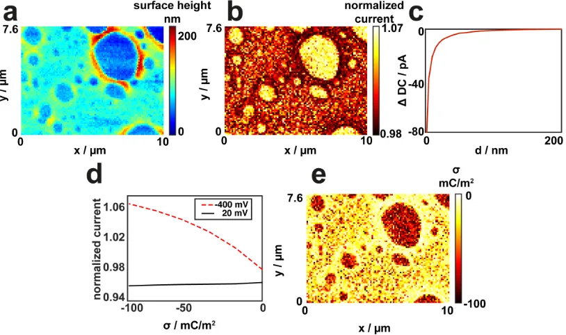
Figure 2.4. SICM-SECM topographical and [Ru(NH3)6] 3+ uptake mapping of a Zea mays root hair cell on a glass substrate ... 55
Figure 2.5. SICM-SECM topographical and [Ru(NH3)6] 3+ uptake mapping of two regions of a single Zea mays root hair cell ... 57
Figure 2.6. Schematic (not to scale) of a 2D slice from the 3D FEM simulation ... 61
Figure 2.7. Difference in the simulated SICM current at a probe-substrate separation distance (d, see above) of 120 nm over substrates of differing uptake rates ... 62
Figure 2.8. Comparison between approach curves ... 63
Figure 2.9. Raw normalized current image of the root hair cell scan presented in Figure 2.5. ... 64
Figure 3.1. Setup for a high-speed charge mapping experiment ... 75
Figure 3.2. Simultaneous topography and quantified charge maps of an incomplete polystyrene film on a glass substrate ... 78
Figure 3.3. Simultaneous topography and charge maps of a PC12 neurite ... 80
Figure 3.4. TEM image of the nanopipette used for the PC12 cell experiments ... 83
Figure 3.5. Schematic of 2D axisymmetric FEM simulation domain ... 84
Figure 3.6. More complete polystyrene scan ... 85
Figure 3.7. Surface charge map of a polystyrene film on a glass substrate collected using the previous bias modulation voltage scanning regime ... 85
Figure 3.8. Normalized current map across the PC12 cell ... 86
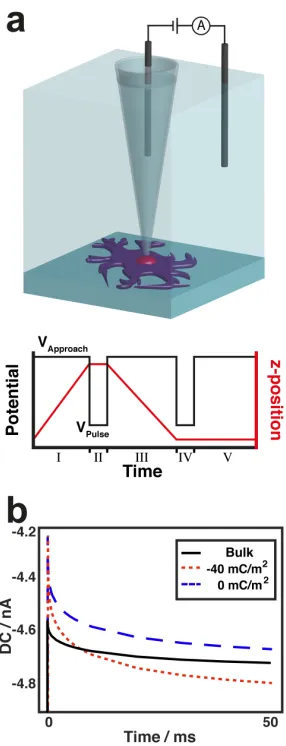
Figure 4.1.Schematic of the potential differences in a ΔC-SICM system ... 97
Figure 4.2. Comparison of electric field strength in conventional and ΔC-SICM ... 98
Figure 4.3.The use of ΔC-SICM as feedback for topographical imaging ... 100
Figure 4.4. Normalized current versus substrate surface charge density for different ... 102
modes and mass transport situations in SICM Figure 4.5. Dependence of electrolyte properties on SICM configuration ... 104
Figure 4.6.Surface charge mapping of PC12 cells using ΔC-SICM ... 106
Figure 4.7. Effect of probe-surface separation on dopamine concentration ... 108
Figure 4.8. Reaction mapping over a CF electrode using ΔC-SICM ... 110
Figure 4.9. Schematic representation of the SICM pulsed-potential method for elucidating surface charge ... 112
Figure 4.10. Schematic of FEM simulation domain ... 113
Figure 4.12. Raw currents corresponding to Figure 4.4 ... 115
Figure 4.13.Surface charge mapping with Etotal = ΔEelectrode + Ejunction ... 116
Figure 4.14. Conversion of raw data into surface charge density ... 118
Figure 4.15. Setup for reaction mapping over an individual CF ... 119
Figure 4.16. Voltammetry of the CF device in 1 mM dopamine hydrochloride ... 120
Figure 5.1. Setup and probe used for copper deposition ... 130
Figure 5.2. Typical z-position and current profiles during a deposition ... 132
Figure 5.3. SEM micrographs (taken at a 45° inclination angle) of copper pillars patterned on gold substrates ... 134
Figure 5.4. SEM images of complex 3D features fabricated with a dual-channel nanopipette ... 136
Figure 5.5. SICM mapping of deposits using the same probe ... 138
List of Tables
Table 1.1. Relationship between electrolyte concentration and double layer thickness
for a 1:1 electrolyte at 298 K ... 22 Table 2.1. Diffusion coefficients of the species simulated ... 60 Table 2.2. Boundary conditions for the FEM model ... 60
Table 2.3. Normalized SECM current values at the distance of closest approach
from a series of approach curves to a Zea mays root hair cell ... 64
Abbreviations
2D Two-Dimensional
3D Three-Dimensional
AC Alternating Current
AFM Atomic Force Microscopy
BM-SICM Bias Modulated Scanning Ion Conductance Microscopy
CF Carbon Fiber
CV Cyclic Voltammogram
CVD Chemical Vapour Deposition
DC Direct Current
DI Deionized (Water)
DM-SICM Distance Modulation-Scanning Ion Conductance Microscopy
DNA Deoxyribonucleic Acid
DTC Doctoral Training Centre
EDL Electrical Double Layer
EFM Electrostatic Force Microscopy
EOF Electroosmotic Flow
EPSRC Engineering and Physical Sciences Research Council
FE-SEM Field Emission Scanning Electron Microscopy
FEM Finite Element Method (Modelling)
FIB Focussed Ion Beam (Milling)
FluidFM Fluid Force Microscopy
FPGA Field-Programmable Gate Array
GC Gouy-Chapman
ICR Ion Current Rectification
IHP Inner Helmholtz Plane
KPFM Kelvin Probe Force Microscopy
MOAC Molecular Organisation and Assembly in Cells
NP Nanoparticle
OHP Outer Helmholtz Plane
ORR Oxygen Reduction Reaction
P-SICM Potentiometric Scanning Ion Conductance Microscopy
QRCE Quasi-Reference Counter Electrode
RPMI Roswell Park Memorial Institute (Medium)
SCE Saturated Calomel Electrode
SECCM Scanning Electrochemical Cell Microscopy
SECM Scanning Electrochemical Microscopy
SEM Scanning Electron Microscopy
SEPM Scanning Electrochemical Probe Microscopy
SICM Scanning Ion Conductance Microscopy
SIR Surface-Induced Rectification
SPM Scanning Probe Microscopy
SPR Surface Plasmon Resonance
STM Scanning Tunnelling Microscopy
STP Standard Temperature and Pressure
TEM Transmission Electron Microscopy
UHV Ultra-High Vacuum
UME Ultramicroelectrode
Acknowledgements
First and foremost, I would like to thank my supervisor Prof. Patrick R. Unwin for
his advice and encouragement throughout the course of my Ph.D. His enthusiasm, be
it for research, music, or running, has provided a constant source of inspiration over
the last three years.
I would like to acknowledge the MOAC DTC via the EPSRC for both their
funding and their support. Thank you in particular to the MOAC 2013 cohort for
making our various trips to conferences and transferable skills courses so enjoyable,
and to Naomi Grew for keeping us all on track when it seems so easy to fall off.
Finally, thank you to everyone in the Warwick Electrochemistry and
Interfaces Group, particularly to Dr. David Perry, Minkyung Kang and Dr. Dmitry
Momotenko, without whom much of the work in this thesis could not have been
completed. Thank you also to all former group members and those in the Chemistry
workshops who contributed to the WEC-SPM platform; your work now facilitates
Declaration
The work presented in this thesis is entirely my own work, except where
acknowledged at the beginning of each chapter. I confirm that this thesis has not
been submitted for a degree at another university. This work is being submitted for
thesis by publication.
Chapter 2 was published as:
Quantitative Visualization of Molecular Delivery and Uptake at Living Cells
with Self-Referencing Scanning Ion Conductance Microscopy-Scanning
Electrochemical Microscopy.
Ashley Page, Minkyung Kang, Alexander Armitstead, David Perry, and Patrick R.
Unwin, Anal. Chem. 2017, 89, 3021-3028. This manuscript also appeared in the
thesis of Minkyung Kang.
Chapter 3 was published as:
Fast Nanoscale Surface Charge Mapping with Pulsed-Potential Scanning Ion
Conductance Microscopy.
Ashley Page, David Perry, Philip Young, Daniel Mitchell, Bruno G. Frenguelli, and
Patrick R. Unwin, Anal. Chem. 2016, 88, 10854-10859. This manuscript also
appeared in the thesis of Dr. David Perry.
Chapter 4 has been submitted as an article to Analytical Chemistry as:
Differential-Concentration Scanning Ion Conductance Microscopy.
David Perry, Ashley Page, Baoping Chen, Bruno G. Frenguelli, and Patrick R.
Unwin, Anal. Chem. 2017, submitted.
Chapter 5 was published as:
Write−Read 3D Patterning with a Dual-Channel Nanopipette.
Dmitry Momotenko, Ashley Page, Maria Adobes-Vidal, and Patrick R. Unwin, ACS
In addition to the above, I have contributed to the following publications that are not
included in this thesis:
Surface Charge Visualization at Viable Living Cells.
David Perry, Binoy Paulose Nadappuram, Dmitry Momotenko, Philip D. Voyias,
Ashley Page, Gyanendra Tripathi, Bruno G. Frenguelli, and Patrick R. Unwin, J.
Am. Chem. Soc., 2016, 138, 3152-3160.
Electrochemical Control of Calcium Carbonate Crystallization and Dissolution
in Nanopipettes.
David Perry, Alexander S. Parker, Ashley Page, and Patrick R. Unwin,
ChemElectroChem, 2016, 3, 2212-2220.
Simultaneous Topography and Reaction Flux Mapping At and Around
Electrocatalytic Nanoparticles.
Minkyung Kang, David Perry, Cameron L. Bentley, Geoff West, Ashley Page, and
Patrick R. Unwin, ACS Nano, 2017, 10.1021/acsnano.7b05435.
And the following review articles:
Frontiers in Nanoscale Electrochemical Imaging: Faster, Multifunctional, and
Ultrasensitive.
Minkyung Kang, Dmitry Momotenko, Ashley Page, David Perry, and Patrick R.
Unwin, Langmuir, 2016, 32, 7993-8008.
Multifunctional Scanning Ion Conductance Microscopy.
Ashley Page, David Perry, and Patrick R. Unwin, Proc. Roy. Soc. A, 2017, 473,
Abstract
Scanning ion conductance microscopy (SICM) is a nanopipette-based technique that
has historically been used for the topographical imaging of soft samples. This thesis
demonstrates the development of SICM into a multifunctional tool, capable of
providing a host of additional information about both biological and inert samples,
whilst maintaining the structural mapping capability for which it is usually
employed.
Two approaches are taken to extend the functionality of SICM: (i) designing
sophisticated potential, and positional, control functions that are then used with
traditional single-channel nanopipettes; and (ii) incorporating an ion conductance
channel into a multi-barrelled probe. In the single-channel setup, a pulsed-potential
profile allows the extraction of surface charge density on extended substrates, and a
ramped-potential profile permits spatially resolved mapping of redox reactions on an
electrode substrate. When integrated into a more complex probe, SICM is used to
study molecular uptake at cellular surfaces, and to print Cu microstructures on a Au
substrate. While this thesis is primarily concerned with technique development, the
studies herein have broad applications in cell biology, pharmaceuticals, materials
science and beyond.
In addition to developing imaging modes that allow the extraction of
functional information at a surface, this thesis also contributes to the fundamental
understanding of the SICM system. Finite element method simulations are
performed alongside experimental studies, in order to fully understand the
contributions of the pipette geometry, ion current rectification, and pipette-surface
interactions on the measured ionic current. The theoretical treatment herein provides
a foundation upon which future multifunctional SICM regimes could be designed,
1
Introduction
1.1 Thesis Summary
This thesis is concerned with the advancement of scanning ion conductance
microscopy (SICM), a scanning electrochemical probe technique first introduced by
Hansma et al. in 1989.1
While SICM has typically been used for topographical
imaging, this thesis focuses on the extension of its capabilities as an ever-more
powerful tool for the investigation both of surfaces, and of ionic fluxes more
generally. The additional functionality brought to SICM by the studies herein
include the incorporation of SICM into a probe to map molecular uptake, the
improvement of SICM as a tool for surface charge mapping, and the use of the
SICM nanopipette to locally deliver and deposit Cu ions to print solid structures.
Each chapter of the thesis has either been published or submitted to a peer-reviewed
journal, and is thus presented in a manuscript format complete with supporting
information. Contrary to the typical thesis layout, this means that each chapter
contains introduction, experimental and conclusion sections and thus constitutes a
complete piece of work.
Chapter 2 demonstrates the combination of SICM with scanning
electrochemical microscopy (SECM) into a single probe in a technique known as
SICM-SECM.2
The SICM channel of this double-barrelled probe is then used both
for topographical feedback and for the local delivery of a molecule of interest. The
SECM channel monitors the local concentration of that molecule as the probe
approaches a surface, with the SECM current dependent on the rate of molecular
uptake at the cellular substrate. This response is then quantified using finite element
method (FEM) modelling that allows the correspondence of the experimental SECM
current to a theoretical uptake rate at the surface.
Chapter 3 of this thesis concerns the development of a new scanning regime
for the use of SICM as a tool for surface charge mapping.3
By improving both the
approach rate of the probe towards the surface, and the potential control function
used to extract surface charge information, the pixel acquisition rate of the technique
increases by an order of magnitude. This enhancement of the scanning speed allows
viability of SICM as a technique for spatially resolved nanoscale surface charge
mapping.
The typical SICM setup (in which both the pipette and the bath contain the
same solution) is perturbed in Chapter 4, in which the effect of having solutions of
differing ionic strength in the tip and the bath is explored. This study demonstrates
that SICM can operate at zero applied bias, as well as in a setup in which the
junction potential at the end of the nanopipette is the only driving force. This new
approach to SICM is capable of both surface charge and local reaction mapping with
equal or superior sensitivity to the standard setup. The additional benefit of a
significantly lower electric field at the end of the nanopipette is also explored using
FEM simulations.
Chapter 5 demonstrates the use of a double-barrel open nanopipette for the
deposition of sub-micron Cu structures on a Au surface.4
One channel is used as a
source of Cu2+
ions, while the other is used for topographical feedback, allowing the
probe to operate as a nanoscopic 3D printer. The technique is used to deposit high
aspect ratio pillars, as well as Γ-like and zig-zag features that are subsequently
imaged using a scanning electron microscope (SEM). The SICM capabilities of the
probe are then utilised to create high-resolution topographical images of the deposits.
The final chapter summarises and contextualises the studies herein, providing an
insight into the possible applications of SICM in future studies.
1.2 Scanning Probe Microscopy
Scanning probe microscopy (SPM) differs significantly from conventional
microscopy in that it does not irradiate the sample, but instead uses a physical probe
to build up an image by moving over the surface.5
There are many different kinds of
SPM, each of which relies on some interaction between the probe and the surface
that is being imaged. In many cases, the information collected may be simply the
surface topography, though some scanning probes are capable of investigating other
interfacial properties such as charge or porosity.
One of the earliest examples of SPM is the scanning tunnelling microscope
(STM, Figure 1.1a),6
which can be used to build atomic-resolution topographical
images of a surface. It relies on the quantum tunnelling of electrons across the gap
known as the tunnelling current.5–7
This current is then maintained at a constant level
as the probe is scanned over the surface. Atomic force microscopy (AFM, Figure
1.1b) uses the deflection of a cantilever to detect the presence of a surface; via either
the attractive or repulsive forces between a tip mounted on that cantilever and the
surface itself.8,9
In addition to the topographical imaging for which it is best known,
AFM can also be used to conduct force measurements at a surface.10–12
While for the
majority of scanning regimes the resolution of AFM is typically not as high as in
STM, it is still several orders of magnitude higher than what could be achieved with
an optical microscope.13–15
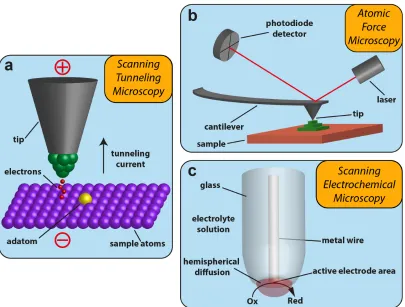
Figure 1.1. Scanning probe microscopy techniques. (a) Scanning tunnelling
microscopy, in which an atomically-sharp conducting tip is brought close enough to
a surface to allow electrons to tunnel across the gap. (b) Atomic force microscopy, in
which a tip is mounted on a cantilever and scanned over a surface, with deflection
monitored using a laser feedback system. (c) Scanning electrochemical microscopy,
in which a microscale wire sealed in a glass sheath is used to detect the local
[image:18.595.118.523.281.588.2]Within the family of all SPMs, some techniques, known as scanning
electrochemical probe microscopies (SEPMs) use an electrochemical signal to detect
a surface. This subfamily includes open-channel techniques such as SICM1,16,17
and
droplet-based techniques such as scanning electrochemical cell microscopy
(SECCM),18–21
though by far the most widely used since its inception in 1989 has
been SECM (Figure 1.1c).22–25
The SECM probe is constructed by sealing a thin
conducting wire (typically a metal such as Pt or Au but may be carbon fiber) of
diameter 1-25 μm inside a glass sheath. The glass is then polished back to reveal the
disc-shaped cross section of the wire, creating a probe known as an
ultramicroelectrode (UME).26
The UME is then used as a working electrode for an
electrochemical reaction (i.e. an oxidation or a reduction), and the faradaic current
measured. As this current is dependent on the local concentration of an
electrochemical species, the probe can be scanned over a surface to build up either a
topographical or functional image.24,27–30
Each of the different scanning probe techniques has several advantages and
disadvantages. For example, STM can provide some of the highest resolution
images, the samples studied often requirement an ultra-high vacuum (UHV). AFM
does not require an UHV, but contact between the probe and the sample makes most
imaging modes (with non-contact AFM a notable exception) unsuitable for many
applications in biological imaging. On the other hand, the SECM probe never comes
into contact with the sample, and has thus been used extensively for live-cell
studies.28,31–35
SECM also opens up the possibility of functional imaging, and it has
been used widely for the visualization of electrochemical activity on electrodes and
other substrates.30,36,37
However, SECM requires than the entire substrate be bathed in
solution, something that is not desirable for all samples. Given the various
advantages of different SPMs, efforts have been made to make hybrid probes that
incorporate several techniques. One example of such a technique is SICM-SECM,38–
41
which allows simultaneous topographical and functional imaging in a single probe.
Other hybrid techniques include AFM-SECM42–45
and STM-SECM,46,47
both of
which aim to correlate structure and function using a single probe.
A common consideration for all SPMs is the resolution that they are able to
achieve, as this determines the samples to which they can reasonably be applied. Of
difficulty of reliably fabricating sub-µm electrodes.48
However, recent advances have
seen some studies in which SECM is extended to the nanoscale.49–54
Powerful
piezoelectric positioning systems and smaller critical probe dimensions allow AFM
to routinely achieve sub-nm resolution, and STM atomic resolution. A second
consideration for SPMs is the speed of image acquisition; as the probe has to
physically raster scan across the surface it can take anywhere from milliseconds to
hours to obtain a single image. This often leads to a trade-off between image
acquisition time and image quality that must be considered and optimised for the
technique and substrate being imaged. Improving the rate of image acquisition in the
use SICM for surface charge mapping is addressed in Chapter 3 of this thesis.
Scanning probe microscopy is a family of techniques that can provide
significant topographical and functional information on both the micro- and
nanoscale that is otherwise inaccessible with conventional microscopy. They have
become integral to the study of many different systems at a diverse range of
interfaces; a rise that is set to continue as their scope continues to widen.
1.3 Scanning Ion Conductance Microscopy
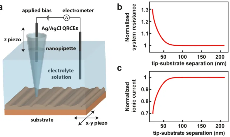
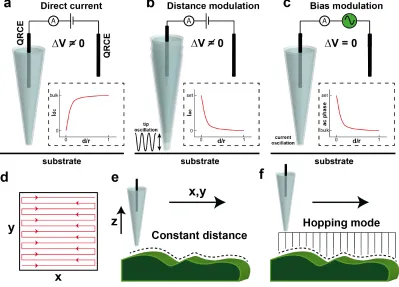
1.3.1 Operation: Scanning ion conductance microscopy (SICM) is a SEPM that
utilises the current between two Ag/AgCl quasi-reference counter electrodes
(QRCEs), one in a glass or quartz nanopipette and the other outside the nanopipette,
as a feedback mechanism when scanning over a substrate (Figure 1.2a).1,16,17
While
SECM has been widely applied to functional imaging,28,50,55
SICM has typically been
used for topographical imaging, as the current flowing between the two electrodes is
sensitive to the probe-substrate separation (Figure 1.2b,c). SICM is used to image a
sample submerged in solution, and is commonly used for living cells.56,57
Another
characteristic that makes SICM particularly suitable to biological imaging is that,
contrary to other SPMs, the probe never comes into contact with the sample, and
thus living systems are not perturbed during scanning. The magnitude of the current
between the two electrodes is determined by both the size of the opening of the
nanopipette as well as the concentration of electrolyte. Typically, the same
electrolyte composition is used in both the tip and the bath, and the high resistance at
the end of the nanopipette governs the current magnitude. An exploration into the
Figure 1.2. Operational principle of the scanning ion conductance microscope. In
the basic SICM setup (a), a bias is applied between two Ag/AgCl electrodes, one in a
glass or quartz nanopipette and the other in the bulk electrolyte solution. The
nanopipette is translated normal to the surface using a piezoelectric positioner (‘z
piezo’), increasing the system resistance at small tip-substrate separations (b). The
increase in system resistance induces a reduction in the ionic current measured at the
electrometer (c). When scanning, the sample is moved laterally relative to the probe
using a two-axis piezoelectric system (‘x-y piezo’).
During a scan, the SICM probe is mounted onto a vertical piezoelectric
positioning system that allows precise movement of the nanopipette normal to the
surface. The sample is mounted onto a two-axis piezoelectric stage that allows the
substrate to move in the x-y plane while the tip remains stationary. One QRCE is
inserted into the nanopipette while a second is placed in bulk solution. In the
standard SICM setup, a bias is then applied between the two electrodes in order to
drive an ionic current.
1.3.2 Feedback Types and Scanning Regimes: While the physical setup remains
the same, there are several methods in which the SICM probe can be used to detect
the surface of interest. The original, and most widely used feedback type is direct
[image:21.595.133.512.78.304.2]towards the surface and the ionic current is monitored for a percentage drop
(typically 1-5%) from the value when the probe was in bulk. This decrease in current
is attributed to the increased resistance in the system, as the gap resistance between
the probe and substrate becomes comparable with that of the probe opening.
The second feedback type used for SICM mapping is distance modulation
(DM, Figure 1.3b). In DM-SICM, an oscillation of the z-position is superimposed
onto the overall movement of the probe. This oscillation is typically at several
hundred Hz with an amplitude of 10-20% of the nanopipette diameter. As the probe
approaches a surface, the oscillation will induce an alternating current (AC)
component of the ionic current that can then be extracted at the same frequency as
the physical oscillation using a lock-in amplifier. The quantity monitored is the
amplitude of that AC signal, which should be zero in bulk and increase upon
approach to the surface as the probe moves repeatedly from high to low current. A
third feedback type, bias modulation (BM, Figure 1.3c), was recently introduced to
SICM imaging.58
In BM-SICM, the harmonic oscillation from the lock-in amplifier
is superimposed on the bias between the two electrodes rather than the z-position of
the probe. This oscillation induces a similar response in the ionic current; the AC
phase of which is extracted and monitored at the same frequency as that applied. The
AC phase is very sensitive to the probe-substrate separation and can thus be used as
feedback for BM-SICM.
Each of the three feedback types has several advantages and disadvantages
that make them suitable to different applications of SICM. DC-SICM typically
allows for a faster approach rate than the oscillation feedback types, as there is no
limitation from the time constant of the lock-in amplifier or potential damage to the
z-piezo. However, the ionic current used for DC-SICM is prone to drifting during
the course of a scan, making it very challenging to operate in a constant-distance
scanning regime (vide infra). DM-SICM overcomes the problem of drift, as the
feedback is reliant only on the change in ionic current during the period of the probe
oscillation, rather than over the course of the entire scan. As BM-SICM considers
only the phase of the AC signal relative to the applied bias, it does not require a net
bias to be applied between the two electrodes. Minimizing the applied bias between
the two electrodes has been shown to be highly beneficial for functional mapping
Figure 1.3. Feedback types and scanning regimes used in SICM. (a) DC-SICM, in
which a decrease in ionic current is used to detect the surface. (b) DM-SICM, in
which a physical oscillation is applied to the z-piezoelectric positioner, and the AC
amplitude of the ionic current increases upon approach to the surface. (c) BM-SICM,
in which a small harmonic oscillation is added to the voltage between the two
QRCEs and the surface is detected via a change in the AC phase. (d) Raster scan
pattern showing the typical path taken by the probe relative to the surface during an
SICM experiment. (e) Constant-distance scanning mode, in which the
probe-substrate separation is kept constant by adjustment of the z-position to maintain a
given feedback threshold. (f) Hopping mode, in which the probe is approached to the
surface at an array of discrete points. Adapted from Page et al.17
Once the appropriate feedback type has been chosen for an SICM
experiment, it is necessary to consider how to scan the probe relative to the surface.
The substrate is typically moved in a raster scan pattern (Figure 1.3d) under the
nanopipette in one of two regimes. In constant-distance mode (Figure 1.3e), the
is achieved by maintaining a constant value of the feedback response, moving closer
to the surface if the feedback needs to be increased, and away if it should be
decreased. In ‘hopping’ or ‘standing approach’ mode (Figure 1.3f), the probe is
translated towards the surface at each pixel of an image, before being retracted into
the bulk solution. While the scan time for hopping mode experiments is significantly
longer than constant-distance mode, it allows the probe to navigate large variances in
topography without breaking the tip, something that can cause difficulties when
using constant-distance mode. Hopping mode also allows functional measurements
(for example uptake rate or surface charge, see Chapters 2 and 3 respectively) to be
referenced to the bulk value at each pixel, which proves necessary when developing
a meaningful quantitative method.
1.3.3 Applications of SICM: The non-invasive nature of SICM relative to other
scanning probe techniques,61
combined with the wide range of potential imaging
media (any ionic species capable of carrying current), have made it a popular
technique for live cell imaging.56,57,62–72
The aim of such experiments is typically to
map the topography of a cell or group of cells, either in their native state or under
some kind of physical or chemical stress. The first images of live cells using SICM
were collected in 1997,73,74 and showed that while there was no damage to the cells
as a result of the SICM probe, changes in surface topography could be detected by
conducting several consecutive scans. The method of performing multiple scans of
the same area of a sample has also been used to study changes in cellular volume and
mobility of cardiac myocytes56
and oligodendrocytes.67
Later studies increased both
the lateral and temporal resolution of the technique in order to study dynamic
processes of subcellular features such as microvilli.64,75
Examples of SICM
topographical imaging of both biological and inert substrates are given in Figure 1.4.
While the topographical mapping of non-conducting, soft samples has
remained the primary use of SICM, it has found several other applications in the 30
years since its inception. In the very first SICM study,1
the nanopipette probe was
used to detect pores in a membrane, with an increase in ionic current attributed to the
increase in local conductance over a pore. This principle has been applied to both
biological76,77
and synthetic78,79
nanopores, and the experimental and theoretical
Figure 1.4. Topographical mapping using SICM. Both the PC12 cell (a) and the
interrupted polystyrene film (b) are on a glass substrate. Adapted from Page et al.17
In addition to the applications of SICM to surface topography and nanopore
conductance, it has also been used as a tool for local delivery to a surface. If the
analyte of interest is charged in solution, the nanopipette can be used as a reservoir
that will deliver on demand depending on the applied electric field. For example, if
the analyte is positively charged in solution, a negative potential can be applied to
the nanopipette QRCE relative to the bulk QRCE, holding the analyte in the probe.
When the nanopipette is located over the desired region of the substrate, the polarity
of the potential can be switched to release the analyte from the probe and deliver it to
a highly specific location. This technique has been used to deliver
negatively-charged DNA molecules from a nanopipette,81,82
and deposit them in microscale
aggregations on a streptavidin-coated glass surface.83
It was subsequently used to
deliver proteins to individual spermatozoa, demonstrating differences in localization
to different subcellular compartments, whilst tracking the delivery using a
fluorescence microscope.84
Recent studies have demonstrated the delivery of
capsaicin to neuronal cells85
and isoproterenol to the T-tubules of cardiomyocytes.86
In this thesis, the SICM nanopipette is used as a reservoir of an analyte to investigate
cellular uptake (Chapter 2), a mediator that is locally delivered to a substrate
electrode (Chapter 4), and Cu2+
ions that are deposited on a Au surface (Chapter 5).
While topographical/nanopore imaging and local delivery have been the most
several other applications. The SICM nanopipette has been used for so-called
‘nanobiopsies’, in which the probe penetrates the cell membrane at a desired point
before extracting a small quantity of intracellular material for further analysis.87
It
was demonstrated that RNA could be taken from the cell, amplified using the
polymerase chain reaction, and then sequenced.87
As the size of the nanopipette used
is much smaller than the overall size of the cell, the technique is minimally invasive
and the cell can remain viable after the nanobiopsy has been performed.
Nanopipettes have also been used as electrospray ionization emitters, with a higher
signal-to-noise ratio than typical nanospray emitters.88
This technique was then
developed into an SPM technique known as scanning electrospray microscopy, that
was used to map topography at the nanoscale.89
Careful control of the voltage regime
used in SICM has allowed it to be used as a tool for surface charge mapping59,60
(see
Section 1.4 and Chapters 3 and 4), and for mapping electrochemical reactions at both
electrode and nanoparticle (NP) substrates.90,91
1.3.4 Understanding the Ionic Current Response: In order to use SICM as a
functional tool for the investigation of interfacial process, it is essential to fully
understand the factors contributing to the experimental observations. These factors
are several, and include the geometry of the nanopipette, the composition of the
electrolyte solution, and the charge on both the tip and the surface.60,92,93
While it is
possible to approach a surface and build up a topographical map without a
comprehensive consideration of each of these elements, it becomes necessary when
attempting to extract functional information using SICM.
1.3.4.1 Probe Fabrication and Geometry: The nanopipette used in SICM is made
from a glass or quartz capillary, typically with an inner diameter of 0.5-1 mm. The
capillary is carefully placed into a laser puller, in which the centre of the capillary is
heated to the point of melting whilst a pulling force is applied to either side. As the
two halves of the capillary are pulled apart, they narrow to a fine point, eventually
separating to create two nanopipettes of similar geometry. The size of the opening at
the end of the nanopipette depends both on the material used and the parameters of
the laser puller, such as the strength of the pulling force and the power of the laser
nanopipettes with the desired aperture, from several microns to several nanometers
in diameter.
During an SICM experiment, the lateral resolution of the scan is directly
linked to the size of the opening at the end of the nanopipette used, and is typically
assumed to be around three times the radius of the opening.93–95
Thus, a probe with a
200 nm diameter aperture would be able to resolve individual surface features of 150
nm in width. With some studies having demonstrated probes with an estimated
aperture radius of 5-10 nm,62,96
this gives SICM a limiting resolution of below 20
nm. While this is significantly higher resolution than can typically be achieved with
SECM, it is still far from the sub-nm resolution routinely achieved with both STM
and AFM. However, SICM has several advantages over both of these techniques in
that the probes are inexpensive and easily fabricated, it can be used on living
samples, and can operate at STP. As a result of these advantages, SICM has been
viewed favourably for soft sample imaging when compared with AFM.61
As the SICM response is highly dependent on the pipette geometry, it is
necessary to characterise the probes produced by a given set of laser puller
parameters. There are several techniques that are used for pipette characterization,
the most common of which is to consider the ionic current response at differing
potential differences in a cyclic voltammogram (CV) regime. The pipette is then
assumed to have a conical shape when calculating the aperture radius from the
current magnitude. A more reliable technique for the study of nanopipette geometry
is scanning electron microscopy (SEM, Figure 1.5a),62,66,89,97
which can provide
structural information about the size of the opening as well as the outer dimensions
of the probe along its length. However, it has been recently demonstrated that the
external geometry alone is not sufficient to fully predict the ionic current response,92
and that the assumption of a conical internal geometry is incorrect. Thus,
transmission electron microscopy (TEM, Figure 1.5b) has become a vital technique
in the full characterization of the SICM probe. TEM provides significantly more
information that SEM as it allows the inner lumen of the nanopipette to be
visualised. This allows many geometrical parameters such as the glass thickness,
diameter and inner cone angle to be extracted along the length of the pipette. The
inner cone angle in particular has been shown to vary significantly along the length
of the pipette,92
Figure 1.5. Electron micrographs of single-channel glass nanopipettes. SICM probes
can be characterised by either SEM (a) or TEM (b).
1.3.4.2 Ion Current Rectification: In the absence of a nanopipette, the ionic current
passed between Ag/AgCl QRCEs in an electrolytic solution follows a linear, Ohmic
relationship with voltage. However, when one QRCE is in the bath and one in a
nanopipette, both the geometry and the surface chemistry of that nanopipette can
affect the magnitude of the current passed. More specifically, the silanol groups on
the surface of the glass or quartz are dissociated at the typical pH values used in
SICM, and they thus present a negative surface charge,98
which in turn gives rise to
an increase in concentration of cations near the surface. The fundamental properties
of charged surfaces are discussed further in Section 1.4, as well as in Chapters 3 and
4 of this thesis. The negative charge, combined with the pseudo-conical geometry of
the probe, gives rise to a phenomenon known as ion current rectification (ICR),99–106
in which there is a nonlinear relationship between the applied bias and the observed
ionic current. The degree to which the current is rectified, termed the rectification
ratio, is dependent on many factors, one of the most significant being the nanopipette
surface charge.92,100,101
Figure 1.6 shows simulated current-voltage curves of a 90
nm-radius nanopipette with different surface charges applied to the nanopipette wall.
The effect of ICR is stronger at higher surface charges, and is reversed in polarity
when the polarity of the charge on the nanopipette is reversed. This is due to the
preferential transport of either anions or cations at a given surface charge polarity. In
ICR also depends on the concentration of electrolyte.99
It is more prevalent at lower
ionic strengths as the layer of solvated ions countering the charge at the surface
extends further into the centre of the nanopipette (see Section 1.4).
Figure 1.6. Dependence of ion current rectification on surface charge. When the
nanopipette is negatively charged, the current is enhanced at negative probe bias and
diminished at positive probe bias. When the charge is positive, the effect is reversed.
As the primary observable quantity in an SICM experiment is the ionic
current, an understanding of the prevalence of ICR in a given experimental setup is
essential if any attempt at quantification of functional information is to be attempted.
Thus, both the relationship between nanopipette charge and ICR, as well as the
separation of pipette-induced and surface-induced rectification have been thoroughly
investigated.3,60,92
1.3.4.3 Finite Element Method Modelling: The complex range of variables that
contribute to the ionic current make the interpretation of the SICM response a
challenging process. In order to provide clarity, a theoretical treatment of the SICM
setup is often performed in tandem with the experiments.60,92
As the partial
differential equations that treat both the transport of species in solution and the
electric field distribution cannot be solved analytically (see Chapters 2 and 4), they
are typically treated numerically to provide approximate solutions with arbitrary
accuracy. One such numerical method is finite element method (FEM) modelling, in
which a one, two, or three-dimensional domain is divided into a finite number of
Multiphysics (used herein). The necessary equations are then solved numerically at
the intersection of the different regions (known as ‘mesh points’) to the desired
degree of error with an iterative solving method.
Designing a FEM model for SICM first requires the reproduction of the
experimental geometry. If both the probe used and the solution domain are
symmetric about their central axis, then SICM can be modelled with a 2D,
axisymmetric geometry, as in Chapters 3 and 4 of this thesis. If the probe is not
symmetric about its central axis, as is often the case with multi-channelled
nanopipettes (see Section 1.3.5), then the experimental setup can be reproduced with
a 3D geometry, as in Chapter 2 of this thesis. It should be noted that 3D simulations
are typically significantly more computationally expensive than 2D simulations, and
thus it is preferable to build models in 2D wherever possible. After the geometry has
been built and the required differential equations included, boundary and initial
conditions are applied. In a SICM simulation, boundary conditions typically refer to
either a concentration or a flux at the interface between two domains, but also
include applied potentials and surface charges. For example, the wall of a
nanopipette would be designated as a ‘zero flux’ boundary as no solution should be
permitted to pass through. The initial conditions are either an initial estimate in the
case of a steady-state simulation, or the starting conditions for a time-dependent
simulation. Time-dependent simulations are typically employed when the system is
perturbed in some way, such as a change in the applied voltage. In order to provide
accurate initial conditions for a time-dependent simulation, it is common to take the
results of a steady-state simulation calculated before the perturbation is applied.
In this thesis, FEM simulations are used to provide a more complete
understanding of the SICM response measured experimentally. In Chapter 2, FEM
simulations are used both to determine the probe-substrate separation in SICM, and
to correlate the observed changed in SECM current with the uptake rate constant at
the surface. In Chapter 3, FEM simulations are used to extract quantitative values of
the surface charge on both inert and cellular surfaces, by studying the relationship of
the ionic current near a charged interface with the magnitude of that charge. Finally,
in Chapter 4, FEM simulations are used to study the change in electric field strength
around the nanopipette tip when the concentration of electrolyte in the probe and the
1.3.5 Multi-channel Probes: In addition to the single-channel applications
described in Section 1.3.3, SICM can be integrated into a multi-channel probe, often
adding greater functionality than can otherwise be achieved with a single barrel. The
simplest multi-channel probe is the ‘theta’ pipette, containing two equally-sized open
channels, each of which is filled with electrolytic solution and a QRCE (Figure
1.7a). This setup has been used for several applications, the earliest of which was the
deposition of two different types of DNA from each of the two channels.107
One
barrel contained DNA labelled with the fluorescent red molecule alexa 647 while the
other was labelled with rhodamine green. Controlling the bias between the two
barrels allowed the selective deposition of the DNA at each pixel, and thus the
printing of two-component images on a functionalised surface. This work is
developed in Chapter 5 of this thesis, in which both the bias between the two barrels
and the substrate bias are carefully tuned to optimise the deposition of Cu
microstructures.
A theta pipette is also used in potentiometric SICM (P-SICM),108–112
which
allows the deconvolution, and thus simultaneous measurement, of both topography
and conductance across a membrane. In P-SICM, electrodes are placed either side of
a membrane in order to induce ion flux across it. One channel of the theta pipette is
then used to track the topography of the substrate, while the other measures the
potential across the membrane, which varies as a function of conductance. This setup
has been applied to both model nanopores108
and biological tight junctions.110,111
The final application of dual open-channel probes is in a technique known as
scanning electrochemical cell microscopy (SECCM). In SECCM, there is no bath
solution, with the probe forming a droplet contact upon approach to the surface, the
morphology of which depends on the tip-substrate separation and the hydrophobicity
of the substrate.18,19
This confined electrochemical cell significantly reduces
background noise relative to a typical SICM experiment, thus increasing the current
sensitivity. SECCM has been used for the study of substrate reactivity,20,113–115
localised dissolution,21,116
Figure 1.7. Multi-channelled nanopipette configurations. When both channels are
filled with electrolyte (a), the probe can be used either in bulk solution or in a
scanning droplet setup. (b) SICM-SECM, in which one barrel is open to solution
while the other is a solid electrode. SICM-SECM can be extended to a quad-barrel
setup (c), with two open channels and two solid electrodes.
The functionality of the theta pipette can be changed by the modification of
one or both of the barrels. One way in which this has been done is to cover one
barrel with a membrane patch containing a single ligand-gated ion channel, which
can then be stimulated by varying the concentration of ligand molecules in the bulk
solution.119
However, the most common modification of a theta pipette is the
deposition of carbon on the inside of one or both barrels, either via pyrolysis120,121
or
chemical vapour deposition (CVD).122–124
While CVD produces probes with a more
consistent geometry, it is both significantly more expensive than deposition via
pyrolysis, and takes many times longer to fabricate a probe. One prominent
application of carbon-filled probes is in SICM-SECM38–41,120,125–127
(Figure 1.7b), in
which one barrel is filled with carbon (SECM) and the other is left open to the bulk
solution (SICM). The carbon is back-contacted with a Cu wire, allowing the
potential at the end of the probe to be varied during a scanning experiment.125,127
SICM-SECM has been used for amperometric measurements of electrocatalytic
activity125,127
and for potentiometric measurements of pH;120
functionality that is
added to in Chapter 2 of this thesis. The sensitivity of SICM-SECM has been
improved by depositing electrocatalytically-active Pt at the end of the carbon
challenging.128
The two-barrel approach used in both SECCM and SICM-SECM has
been extended into a four-barrel ‘quad-probe’ (Figure 1.7c), with two open channels
that create a droplet on the surface, and two individually-addressable carbon
nanoelectrodes.129
This setup has been used to investigate the electrochemical
activity of individual carbon nanotubes,129
and to detect single molecules with
femtoamp precision.130
Chapter 2 of this thesis is concerned with the use of a
multifunctional probe in a SICM-SECM configuration for the detection of molecular
uptake on a subcellular scale.
1.4 Surface Charge
Surface charge is a phenomenon in which a surface has either a net positive or a net
negative density of charged species such as electrons or ions. It is often considered in
the study of colloids, in which the presence of an external charge on colloidal
particles can increase repulsion between particles and thus improve the stability of
the suspension as a whole.131
However, it can also be manifest on extended surfaces
such as glass or quartz,98,101
or in living systems such as proteins and biological
membranes.132,133
The presence of charge on a surface can arise from several different
physical phenomena; the adsorption of charged ions onto a surface, protonation or
deprotonation of surface groups, and, in the case of a conducting surface, the
application of an external voltage. The magnitude of charge on a surface is
normalised to the area of the substrate to give a quantity known as the surface charge
density, measured in units of C m-2
. These units make it possible to imagine surface
charge as the number of elementary charges, e, per unit area. While this may be the
case for fixed surface groups of which some fraction may be
protonated/deprotonated in a given set of conditions (for example, variable pH), this
approximation is less appropriate for non-fixed charges, such as those within a metal
under an applied potential. In addition to the importance of surface charge in colloid
chemistry, it can also play a crucial role in nanoscale devices such as solid-state
nanopores,104,134
as well as in crystalline systems.135–139
Surface charge is also important in many aspects of cellular function.
Oligodendrocytes of the central nervous system were shown to down-regulate the
production of negatively charged oligosaccharides of the glycocalyx when wrapping
to multi-cellular stacking, with weak, long distance attractive forces being allowed to
dominate.140
The adhesion of both E. coli and other bacteria have also been shown to
have a strong dependence on charge interactions.141,132
The variation of surface
charge density and polarity is a common feature of studies that consider the uptake
of NPs into living cells, with different surface functionalities providing different
uptake rates and levels of cytotoxicity.142–145
Charged polymers have been used to
direct and control cellular growth and morphology,146 and charged groups within the
membrane of budding yeast cells have been used to guide division via the
application of an external electric field.147
In addition to cellular adhesion, uptake,
and growth, surface charge has been shown to play a role in intercellular
communication, notably in the cases of cancer cell exosome internalization148
and
T-cell activation.133
Chapter 3 of this thesis explores the charge density across the
surface of neuron-like PC12 cells using SICM.
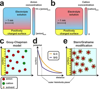
1.4.1 Double Layer Theory: The presence of a charged interface under electrolyte
solution causes a perturbation of the solution composition near the charged
surface.149
For example, a surface that presents a positive charge in a given set of
conditions would induce a higher concentration of anions near the surface, and a
depletion of cations (Figure 1.8a,b). The region near the surface in which the
composition of the electrolyte is altered from bulk solution is termed the diffuse, or
electrical double layer (EDL). The composition and size of the EDL are highly
sensitive to the nature of the surface (e.g. conducting or insulating), the magnitude of
the charge on the surface, and the concentration of electrolyte in the bath solution.150
Much of the foundational work in the study of charged interfaces was motivated by
the relationship between applied potential and surface charge at electrode
surfaces.151–153
While the applications in this thesis typically consider the charge
presented at either insulators such as glass, or in more complex systems such as
living cells, the basic principles described herein are transferable between the
Figure 1.8. Structure of the electrical double layer (EDL). The general situation at
the interface of a charged surface and an electroneutral solution is the perturbation of
ionic concentrations from bulk concentration near the surface (a,b). For a
positively-charged surface, there is an increase in anion concentration (a) and a decrease in
cation concentration (b) adjacent to the surface. The Gouy-Chapman (GC) model of
the EDL (c) does not consider the finite size of ions and is thus unsuitable at high
electrolyte concentrations. Modifications of the GC model by Stern and Grahame
account for phenomena such as specifically-adsorbed ions and a solvent layer at the
surface (e). Plots of the electric potential that arise from the charge at the surface (d)
differ between models depending on the treatment of the ions closest to the interface.
The first person to realise that the introduction of a charged surface into an
electrolytic solution would cause a rearrangement of ions near that surface was
Helmholtz, and he demonstrated the first notion of the EDL as a nanoscale dielectric.
charge stored by the EDL was linearly dependent on the applied potential, a notion
disproved independently by Gouy and Chapman in the early 20th
Century. The
Gouy-Chapman (GC) model of the EDL introduced the idea of a diffuse layer of
ions close to the interface in order to balance out the charge on the surface (Figure
1.8c). This diffuse region of counterions is at its highest concentration directly
adjacent to the surface, while the concentration is lower at greater separation due to
the reduction in strength of electrostatic forces. This leads to an exponential drop in
the electric potential away from the surface (orange line, Figure 1.8d), the profile of
which is dependent on many factors including the magnitude of the surface potential
and the concentration of electrolyte species. For example, if the concentration of
electrolyte is very low, the characteristic length of the EDL will be relatively long as
the volume required to provide the counterions needed to balance a charge at the
surface is larger than in a high concentration solution. In the GC model, the
relationship between the surface charge density (!!) and the surface potential (!!) is
given by the following:154
!! = (8!"#!!!×10!)! !sinh !!!"!!! (1.1)
where ! is the molar gas constant, ! the temperature, ! the dielectric constant of the
solvent (78.54 for water at 298 K), !! the permittivity of free space, ! the molar
concentration of electrolyte, ! the charge magnitude of the !:! electrolyte used, and
! the Faraday constant. This model of the EDL is best applied in systems with low
ionic strength and at low potentials.149
At low ionic strength, the use of the dielectric
constant of water is a reasonable approximation (for an aqueous solution), but this
becomes far less accurate as the concentration is increased. At low surface
potentials, the model predicts reasonable electrolyte concentrations near the
interface, but the omission of the finite size of the ions in solution means that it can
be unrealistic at high surface potentials, when the number of ions required to balance
the charge at the surface is large. Despite these limitations, the GC model can be used to extract the Debye parameter (!), the inverse of which is described as the
!= !!!"#!!×!"! !
!
!
!
(1.2)
where ! is the ionic strength of the electrolyte solution. As described above, ! is
proportional to the square root of the ionic strength, and thus the thickness of the
EDL will decrease as the ionic strength increases. Table 1 shows some values of
double layer thickness, !!!, for several different 1:1 electrolyte concentrations at
[image:37.595.233.406.296.429.2]298 K.
Table 1.1. Relationship between electrolyte concentration and double layer thickness
for a 1:1 electrolyte at 298 K.150
! (mM) !!! (nm)
0.1 30.4
1 9.62
10 3.04
100 0.96
1000 0.3
To accommodate for the breakdown of the GC model at high electrolyte
concentrations and surface charges, Stern proposed a modification that incorporated
many of the ideas of Helmholtz. He realised that ions have a finite size, that an ion
could not approach closer than an ionic radius, and that they could thus not be
treated as point charges. He proposed a compact layer directly adjacent to the
electrode, now known as the Stern layer, comprised of solvated ions at the point of
closest approach (Figure 1.8e). The plane passing through the middle of those
solvated ions is termed the outer Helmholtz plane (OHP). As the thickness of the
Stern layer is pre-determined by the electrolyte and solvent used, the exponential
decay in electric potential seen in the GC model does not occur, and the drop in
potential from the surface to the OHP is instead linear (blue line, Figure 1.8d). The
diffuse portion of the EDL outside of the Stern layer is still treated with the GC
model, and the electric potential at the OHP is significantly lower than at the surface.
Grahame suggested the inclusion of a second plane (now known as the inner


![Figure 2.4. SICM-SECM topographical and [Ru(NH3)6]3+ uptake mapping of a Zea](https://thumb-us.123doks.com/thumbv2/123dok_us/9459864.452754/70.595.151.495.73.466/figure-sicm-secm-topographical-ru-uptake-mapping-zea.webp)