Implementation of CMOS Low-power Integer-N
Frequency Synthesizer for SOC Design
Debashis Mandal and T. K. Bhattacharyya
Email: [email protected], [email protected]
Abstract— The paper reports the implementation of a fre-quency synthesizer for system-on-chip (SOC) design. The epi-digital CMOS process is used to provide SOC solution. This work focuses on low-power consumption to achieve longer life-time of batteries. A 2.4GHz frequency synthesizer has been fabricated in0.18µmepi-digital CMOS technology for ZigBee applications, which consumed 7.95mW from 1.8V supply. The synthesizer has achieved phase-noise of −81.55dBc/Hzand−108.55dBc/Hzat 100kHz and 1MHz offset, respectively. The settling time measured is less than
25µs for an output frequency change of 75MHz from 2.4GHz. The chip core area is0.75×0.65mm2.
Index Terms— Frequency synthesizers, phase locked loops (PLLs), oscillators, integer-N topology, ZigBee standards, system-on-chip solution, low-power design.
I. INTRODUCTION
The wireless communication market has been growing very fast due to ever emerging new applications which demand small-size, low-cost, long-battery-life solution. To provide small-size, low-cost solution, many efforts have been made to integrate the whole system in a low-cost technology. The improvement of technology and design is also driving down the cost. The application area of wireless communication includes wireless local area network (WLAN), global positioning system (GPS), cord-less phones, mobile phones, remote control toys, home automation, etc. There exists different communication standards, for example: Bluetooth, ZigBee, GSM, CDMA, Wi-Fi, WiMAX, HomeRF and so on, which are optimized for different implementations.
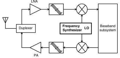
The local oscillator (LO) is an important part of any wireless communication system as shown in figure 1. It is used to up or down convert the transmitted or received sig-nals. For example, in a conventional heterodyne receiver a tunable local oscillator at radio frequency (RF) is mixed with received RF signal, shifting the RF signal to a fixed intermediate frequency (IF) signal. To achieve this, the LO should be tunable and very stable. The popular PLL-based frequency synthesizer is generally used as the local oscillator.
This paper is based on “7.95mW 2.4GHz Fully-Integrated CMOS In-teger N Frequency Synthesizer,” by D. Mandal and T. K. Bhattacharyya, which appeared in the Proceedings of the 20th International Conference on VLSI Design (VLSID) held jointly with 6th International Conference on Embedded Systems, Bangalore, INDIA, January 2007. c 2007 IEEE.
D. Mandal and T. K. Bhattacharyya are with the Department of Electronics and Electrical Communication Engineering, Indian Institute of Technology Kharagpur, Kharagpur-721302, INDIA
Frequency Synthesizer LO
Baseband subsystem Duplexer
LNA
PA
Figure 1. Frequency synthesizer as LO in wireless transceiver system
This paper presents the implementation of CMOS low-power integer-N frequency synthesizer for SOC design complying 2.4GHz ZigBee standard. ZigBee is an indus-try standard for short range, low bit rate, cost, low-power wireless applications. 2.4GHz ZigBee specifies 16 channels with spacing of 5MHz in the frequency range of 2.4GHz to 2.4835GHz. The power consumption of the most power consuming blocks, like VCO and frequency divider, in frequency synthesizer has been reduced by improvising the design approach while keeping other performances (noise, spur, settling time) within acceptable limit.
The motivation behind this work is given in section II. Section III includes the publications relevant to this work. Section IV discusses the architecture chosen for the frequency synthesizer realization. Building blocks of frequency synthesizer are explored in section V. In section VI experimental results are given. Finally, it is concluded in section VII followed by acknowledgment.
II. MOTIVATION
The board level integration of several high quality dis-crete components does not provide the low-cost solution because high component count and multiple chips in various technologies increase the cost. Thus, the ultimate goal is a single-chip-realization with minimum number of off-chip components. However, many difficulties remain in the process of integration due to the lack of high quality on-chip components.
a system-on-chip (SOC) design. This implies a high re-liability of frequency synthesizers implemented in digital CMOS process.
The phase-noise is a measure of spreading of spectrum around the desired frequency and an important param-eter of oscillator’s performance measurement. The RF frequency synthesizer utilizes a low-phase-noise [9] LC voltage controlled oscillator (LC-VCO) which contributes the frequency synthesizer’s out-of-band (frequencies more than synthesizer’s loop bandwidth) phase-noise. The ref-erence signal source, used as refref-erence frequency for syn-thesizer and frequency comparison process, contributes the in-band phase-noise. Thus, for frequency synthesizer’s low bandwidth, VCO phase-noise is critical. To keep the phase-noise of VCO low, the LC-tank quality factor, which is mainly dominated by quality factor of inductor, should be kept high. But the quality factor of inductor, realized on digital process, is very low. Low quality factor degrades the phase-noise performance and also increases the power consumption. More power consumption de-creases the life-time of battery used in portable devices in wireless communication systems.
To handle the issues of life of batteries and problems related to heat generation in continuously shrinking ICs, the power consumption has become a major concern to address in today’s low-cost wireless systems. Specially for the low data rate short distance wireless communication standards, systems with moderate performance but very low power consumption are demanded. ZigBee is an example of such standards.
The frequency synthesizer is one of the most critical building blocks for any integrated wireless system and its design challenges are increasing day by day with the increasing demand for high frequency, power constrained and cost effective solution for wireless systems. The aim of this work is to design a very low-power ZigBee compliant frequency synthesizer for SOC design.
III. BACKGROUND ANDRELATEDWORKS
Significant work has been carried out over the last few years in the field of frequency synthesizers for differ-ent applications. The performances of 2.4GHz integer-N frequency synthesizers reported in [1], [2], [3], [4], [5], [6], [7], [8] are summarized in table I. From the table, it is observed that for the frequency synthesizer in [8], the settling time has been reduced to less than 10µs (simulated) for 80MHz frequency jump from 2.4GHz by using two-point channel control namely divider control and direct VCO control. Also the power consumption of this design is quite low (simulated value is 3.48mW from 1V). But the frequency synthesizer has been realized using RF-CMOS process which is not favoured in digital circuit realization for SOC design. Frequency synthesizers reported in [1], [3], [4], [5] and [6] have been realized in standard CMOS process. The power consumption of the synthesizer in [6] is 8mW but the off-chip loop filter has been used due to its large capacitance requirement. Also for the designs in [1] and [2], off-chip loop filter has been used. The phase-noise is small for the design [7] but realized in RF process. The phase noise performances of all other designs reported in the table are moderate. The off-chip VCO and programmable divider have been used in the synthesizer in [4].
The conventional MOS varactor has been used in the frequency synthesizers in [1], [2], [3], [5], [6] and [7]. The frequency of the LC-VCO with conventional MOS varactor varies linearly over a small tuning voltage range. This requires large VCO gain (KV CO) to cover the
required output frequency range. A largeKV COincreases the noise contribution of phase frequency detector, charge pump, divider and input reference frequency source at synthesizer output. Therefore, lowKV COis desirable. In addition, largeKV COvariation over the tuning range can introduce problem in loop stability and settling time. The
TABLE I.
PERFORMANCE SUMMARY OF DIFFERENT REPORTED WORKS
Process Type, Frequency Loop- Phase noise Reference Settling time Power Applications
Ch. spacing range filter spurs consumption
Ref. [1] [2001] 0.35µm Integer-N, 2.4-2.5GHz off-chip -116dBc/Hz −53dBc ≈140µs – at 2.7-3.3V Bluetooth
(Measured CMOS 1MHz at 2MHz offset
results)
Ref. [2] [2003] 0.2µm Integer-N, 2.4GHz off-chip -104dBc/Hz – <600µs(for 17mW at 1V Bluetooth
(Measured CMOS/SOI 1MHz Bluetooth at 1MHz offset 100MHz jump)
results)
Ref. [3] [2003] 0.25µm Integer-N, 2.4-2.527GHz on-chip -112dBc/Hz −58.7dBc ≈60µs(for 20mW at 2.5V Bluetooth
(Measured Digital 1MHz at 1MHz offset 64MHz jump)
results) CMOS
Ref. [4] [2003] 0.25µm Integer-N, 2.4GHz on-chip -105dBc/Hz −62dBc ≈30µs(for –, VCO at 5V, Bluetooth
(Measured CMOS 1MHz Bluetooth at 0.55MHz offset 100MHz jump) Test-chip
results) at 3V
Ref. [5] [2004] 0.25µm Integer-N, 2.4-2.48GHz – -115.9dBc/Hz – <100µs(for 14mW at 1V Bluetooth
(Simulation CMOS 1MHz at 1MHz offset 80MHz jump)
results)
Ref. [6] [2005] 0.18µm Integer-N, 2.1-2.4GHz off-chip -98.7dBc/Hz – ≈50µs(for 8mW at 1.8V Wireless
(Measured Standard – at 0.5MHz offset 100MHz jump) sensor
results) CMOS
Ref. [7] [2005] 0.35µm Integer-N, 2.28-2.75GHz – -117dBc/Hz – <100µs 66mW at 3.3V –
(Simulation RF process – at 0.6MHz offset
results)
Ref. [8] [2005] 0.18µm Integer-N, 2.4-2.48GHz – -112dBc/Hz – <10µs(for 3.48mW at 1V ZigBee
(Simulation RF-CMOS 5MHz at 1MHz offset 80MHz jump)
distributed MOS varactor biasing scheme [10] has been used in [8] to reduceKV CO and its variation.
In the presented work the power consumption of LC-VCO has been reduced by implementing high value inductance in the LC-tank. While divider power consump-tion has been improved by designing it as a combinaconsump-tion of both power consuming analog cells and power efficient static logic. AlsoKV COhas been reduced by using a new linearization circuit in VCO tuning voltage path.
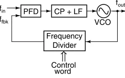
IV. ARCHITECTURE
PLL-based architecture has become very popular for modern frequency synthesizer implementation. The basic block diagram is shown in figure 2. It consists of a phase frequency detector (PFD), a charge pump (CP), a loop filter (LF) and a voltage controlled oscillator (VCO) in the feed-forward path and a programmable frequency divider in the feed-back path. The phase frequency detector acts as an error detector to sense the phase error between the input reference signal and the VCO output signal after being divided by the programmable divider. The tuning voltage of the VCO will be dynamically adjusted by the charge pump and loop filter until the synthesizer is locked. Under the phase-locked condition, synthesizer’s output frequency fout is N times the input reference frequency fin, where N is the division ratio. Therefore, the frequency synthesizer generates multiple frequencies (N fin) from the input reference frequency by varying division ratio.
PFD CP + LF VCO
Frequency Divider fin
fout
ffbk
Controlword
Figure 2. Block diagram of frequency synthesizer
In integer-N type architecture the programmable divider changes division ratio only in integer steps. Hence, it is necessary that the input reference frequency must be equal to the desired frequency step. For narrow-band systems, the input reference frequency should be limited to the channel spacing requirement, while the division ratio should be large enough for the VCO to be locked with respect to input reference frequency. Such a large division ratio results in larger power consumption for the divider and larger phase-noise at the synthesizer output. Moreover, integer-N architecture is known to have frequency resolution versus settling time trade-off. This is because to ensure the stability of the system, the loop bandwidth is typically limited to less than one-tenth of the input reference frequency. As the settling time is inversely related to the loop bandwidth, the settling time is limited by the loop bandwidth.
As per ZigBee standard the channel spacing is 5MHz, which is relatively wider. And the required settling time
is less than 192µs (12 symbol periods), which is also relaxed. Further, ZigBee is a low-cost and low-power application standard. Hence, relatively simple integer-N architecture is adopted for the design to reduce both the power consumption and the silicon area.
V. BUILDINGBLOCKS
A. Voltage Controlled Oscillator (VCO)
Voltage controlled oscillator (VCO) is one of the most critical building blocks in the design of frequency syn-thesizer. LC tuned VCO is used to achieve the oscillation at high frequency with lesser phase-noise compared to the ring oscillator. On the other hand, on-chip inductor on epi-digital CMOS process has very low quality (Q) factor that increases the power consumption. Low Q-factor also degrades phase-noise performance. On-chip inductor takes large silicon area and LC-VCO provides narrower frequency tuning range over the ring oscillator. The phase-noise of the VCO is dominant in the whole system at frequency offsets beyond the synthesizer’s loop bandwidth.
SCA
Mn1 Mn2
Mp1 Mp2
Mp3 Mp4
L0 SCA
Vctrl
Vout
+
-Vdd
ibias
[from reference generator]
Mn4 Mn3
R0
Mn0
Figure 3. Voltage controlled oscillator
cross-coupled transistors, should be tuned such that at resonance frequency, ω0, the real part of the equivalent admittance (Y(jω0)) across the LC-tank must be less than zero. This gives the condition of gm ≥ R1
p, where Rp
is the equivalent parallel resistance of the LC-tank. In the circuit the constant tail current source, realized by transistorMn3, reduces VCO signal swing variation over the process variation.
PMOS transistors pairMp3-Mp4acts as MOS varactor in the circuit. MOS varactor gives capacitance variation over a narrow voltage range. This tuning voltage (Vctrl) range has been extended by connectingVctrl to the MOS varactor through a voltage amplifier whose voltage gain is kept less than unity. Here it has been realized by a common source amplifier with resistive load (Mn0,
R0 in figure 3). This amplifier has been designed such that it maps the desired loop filter output voltage (Vctrl) range to MOS varactor input voltage range, over which VCO frequency varies linearly. Thus, the MOS varactor combined with the common source amplifier (called as linearization circuit) extends the linear range of VCO tun-ing voltage in the VCO frequency versus tuntun-ing voltage characteristic. Therefore, it reduces VCO gain (KV CO). The smallKV CO reduces the contribution of noise from loop filter, charge pump, PFD, divider and input reference frequency source at the output of synthesizer. Hence, more noise from the loop filter may be allowed because any change in the tuning voltage has little effect on the capacitance of the varactor and the frequency of the VCO due to lowKV CO. As a result, much smaller on-chip loop filter capacitors have been used to filter out the noise, reducing silicon area requirement. But the implemented linearization circuit suffers from the following drawbacks: i) circuit is sensitive to process variation and ii) power consumption varies withVctrl voltage level.
To get the variation of 75MHz frequency band (as per ZigBee specification) at synthesizer output with low KV CO, switched-capacitor array (SCA) [11] has been used in the design of the VCO (figure 3). Switches in SCA are controlled digitally by the control word which changes division ratio of the programmable divider. The 75MHz frequency band has been divided into eight subbands and the SCA tunes the VCO operating frequency in the subbands depending on the digital control bits of the division control word. In addition, the SCA also helps to get a faster switching time.
VCO voltage gain (Av) can be expressed as Av = gmRp, where equivalent parallel resistanceRpof the LC-tank is typically dominated by the loss of the inductor in advanced sub-micron CMOS technology. Because the quality factor of the capacitor is usually high (more than 30), so the loss of the capacitor can be ignored. Therefore, Rp can be expressed as Rp ≈ RsQ2L, where inductor quality factor QL is ω0L/Rs and L is the inductance. With the increment of L value, inductor series resistance Rs also increases. It is assumed that the inductor quality factor is constant at operating frequencyω0. This gives a constant RLs ratio, which is represented by K. Then, the
VCO voltage gain is written asAv=gmω02KL. Thus, for a fixed VCO frequency the voltage gain is proportional to the inductance i.e. Av ∝ L. Hence, for same power consumption the higher inductance increases the VCO voltage gain and hence the voltage swing. In other way, the higher inductance reduces the power consumption for the same voltage swing.
In the above design 4.5nH symmetrical, differential, spiral, square shape on-chip inductor has been used. In-ductor has been realized with metal 5 and simulated with Asitic and IE3D softwares. Simulation through Asitic and IE3D, shows Q value of 4.9 and 4.3 respectively. KV CO has been kept around 60MHz/V in the design. To take care the VCO frequency shift due to the variation of inductance and process, externally controlled SCA has also been used. The designed VCO typically consumes around 2.6mA current from 1.8V supply with Vctrl = 1.2V in simulation. Source follower buffers have been added to the VCO outputs to test the VCO output signals.
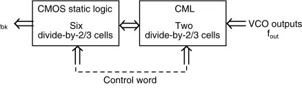
B. Programmable Frequency Divider
It is important to include the divider that can operate at high frequency signal of the VCO to track the VCO output signal and to lock the synthesizer. The high frequency divider consumes more power than the low frequency divider. On the other hand, after first few high frequency dividers, signal frequency becomes low enough that low frequency dividers can be used. The Programmable fre-quency divider block as shown in figure 4, has been implemented with a combination of power consuming current mode logic (CML) for high frequency division and power efficient CMOS static logic for low frequency division.
Six
CML
Two
divide-by-2/3 cells
divide-by-2/3 cells
ffbk
Control word
fout
VCO outputs CMOS static logic
Figure 4. Divider block diagram
Divide-by-2/3 cell based topology [12] has been chosen for realization because this architecture is modular and regular in nature and hence convenient for designing. For such a divider, which consists of n number of divide-by-2/3 cells, the output signal time period (Tdiv−out) is expressed as a function of the input signal time period (Tdiv−in) by
Tdiv−out = (2n+ 2n−1pn+ 2n−2pn−1+....
....+ 21p2+p1)Tdiv−in
where pr is the division control signal of therth divide-by-2/3 cell. The control bit pr can be either ‘1’ (high) or ‘0’ (low). When pr = 1 the rth divide-by-2/3 cell
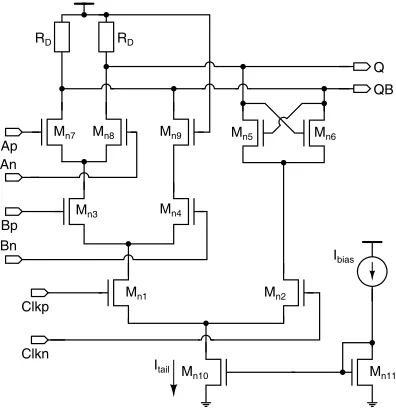
first two divide-by-2/3 cells near to VCO, which work at high frequency signal of the VCO, have been realized based on CML. For the remaining six divide-by-2/3 cells, which work in low frequencies, CMOS static logic has been used. The CML is a non-saturation constant-current reduced-swing logic that makes it enable to operate at high frequency than a CMOS static divider but it con-sumes more power [13]. On the other hand, static logic needs rail-to-rail input signal swing for faithful operation. Therefore a comparator with low power consumption has been implemented as interface circuit between CML and CMOS static logic. To further reduce the power consumption, the AND operation is combined with CML latch [12]. A circuit diagram of such CML latch with AND/NAND gate is shown in figure 5. Transistor Mn10 provides the tail current for the CML latch.
Mn1 Mn2
Mn3 Mn4
Mn5 Mn6
Clkn
Q
RD RD
Clkp Mn8
Mn7
An Ap
Mn9
Bp Bn
Mn10
QB
Mn11
Ibias
Itail
Figure 5. AND/NAND gate combined with CML latch
The tail current for the fastest CML latch circuits has been kept around 190µA and the value of load resistance is 4kΩ. To keep the same output swing, the tail current and the load resistance of CML latches in the consecutive stage have been halved and doubled, respectively. Simulated typical power consumption of the full divider block is around 1.5mA from 1.8V supply. The programmable divider’s output which goes to the phase frequency detector has been taken out through a buffer for the test purpose.
C. Phase Frequency Detector (PFD)
The conventional sequential three-state D-flip-flop based PFD [11], [14], shown in figure 6(a), has been implemented. It provides large linear detection range and also indicates sign and magnitude of the frequency error. The output signals drive the switches of charge pump. Therefore, the narrow up or down pulse at PFD outputs, which corresponds to very small phase error, may not find enough time to reach a logical high level due to the capacitance seen at its outputs (‘up’ and ‘dn’). This
DFF D rst Q fin
ffbk
‘1’
delay
up
dn
in inv out
transmission gate DFF
D rst Q ‘1’
out
(a) (b)
Figure 6. (a) Phase frequency detector, (b) buffer
phenomenon is called as ‘dead zone’ problem [11], [14]. This problem is eliminated by allowing significant amount of equal pulse width at up and down signals on phase-locked state such that the switches of charge pump can turn on properly for small phase error. This is usually achieved by adding additional delay after AND gate (figure 6(a)).
To drive the switches of charge pump in figure 7, the complementary signals with equal propagation delay are required. The buffer shown in figure 6(b), has been used at the outputs ‘up’ and ‘dn’ to generate the complementary signals with equal propagation delay.
D. Charge Pump (CP)
The charge pump circuit of figure 7 has been realized. It sinks and sources current into the loop filter based on the outputs of the PFD. In the circuit transistorsMU P and MDN provide up and down currents those are combined to generate the required net current. Transistors MS1, MS2,MS3 and MS4 act as switch and steers the charge pump up and down currents into the loop filter. The unity-gain amplifier U1 with switches MS3, MS4 reduces the charge sharing problem [14] which results in the reduction of spurs at the synthesizer output. Also the mismatch between up and down currents should be minimized to reduce reference spurs [15] at frequency synthesizer out-put. TransistorsMS3andMS4have the same dimensions of MS1 and MS2, respectively. Transistors Mdm1 and
ICP-out
MUP
MDN MS3
MS4
MS1
MS2
n1
n2
n3 ibias
UP
UPB
DN DNB
UP
DNB ICP
ICP
Mn1
Mp1 Mp2
Mp3 Mp4
U1
+ -Mdm3
Mdm4
Mdm1
Mdm2 out
Mdm2are connected to node ‘out’ to suppress the charge injection at this node. When MS1 (MS2) turns off it injects charge to node ‘out’ and that charge is taken out by Mdm1 (Mdm2) by turning it on, and vice versa. The
size ofMdm1 (Mdm2) should be kept at half of the size
of MS1 (MS2). Transistors Mdm1 and Mdm2 also help
to reduce the clock feed-through problem. In the similar way, to reduce the charge injection and clock feed-through problems at node n1, transistors Mdm3 and Mdm4 are added to this node. The size of Mdm3 and Mdm4 is tuned at half of the size of MS3 and MS4, respectively. In the design the charge pump current (ICP) has been kept around24µA.
E. Loop Filter (LF)
Loop filter is usually used in frequency synthesizers not only to convert charge pump output current to VCO tuning voltage, but also to filter out the noise from the VCO tuning voltage. Higher order loop filter further suppresses the ripples at its output. But from the system stability point of view, lower order loop filter is preferred. Thus, the choice of loop filter for synthesizers is critical. The third order passive loop filter, shown in figure 8, has been implemented and the total synthesizer has become a fourth order type II system.
C1
C2
R2
R3
C3
ICP-out Vctrl
Figure 8. Third order passive loop filter
The values of the loop filter components have been derived from the frequency synthesizer loop stability analysis. To reduce the complexity of the analysis, first the second order loop filter has been considered. Second order loop filter consists of onlyR2,C1and C2.
Transfer function of the second order loop filter is
Z(s) = 1 C1+C2
(1 +sR2C2) s
1 +sR2C1C2
C1+C2
where time constants for zero and pole are
Tz=R2C2 and Tp= R2C1C2
C1+C2, respectively.
Replacing s=jω the complete open-loop transfer func-tion of the synthesizer is expressed as
G(jω) = ICP 2π
KV CO jω
1 (C1+C2)
(1 +jωTz) jω(1 +jωTp)
1 N
The phase ofG(jω)is represented by
G(jω) =tan−1(ωTz)−tan−1(ωTp)−180◦
Hence, obtained phase margin is
φ(ω) =tan−1(ωTz)−tan−1(ωTp)
⇒ dφdω = Tz
1 + (ωTz)2 − Tp 1 + (ωTp)2
Now, dωdφ = 0 gives a maxima in the phase margin at ωm= √1
TzTp frequency. To obtain the maximum phase
margin (φ0), the phase margin maxima should occur at the synthesizer open-loop unity-gain cross over frequency (ωc)i.e.ωc=ωmand atωcfrequency open-loop transfer function becomes
(C1+C2) = ICPKV CO 2πN ωc2
1 + (ωcTz)2 1 + (ωcTp)2 The time constants (Tp,Tz) can be written as a function
of phase margin (φ0) and open-loop unity-gain frequency (ωc)as
Tp= secφ0−tanφ0
ωc and Tz =
1 ωc2Tp
From the above equations, for a target bandwidth of ωc and phase margin ofφ0 the values ofR2,C1 andC2are obtained as
C1= Tp
Tz(C1+C2) ; C2 =
Tz Tp −1
C1; R2 = Tz C2
These relations give the starting values of R2, C1 and C2 for a third order loop filter. Then, the values of R3 and C3 have been chosen such that the pole contributed by these is placed equal or more than ten times of open-loop unity-gain frequency. From the stability analysis with MATLAB simulator, the values of R2,C1, C2, R3 and C3have been tuned for the targeted open-loop unity-gain bandwidth (UGB) and phase margin. The design has been optimized with MATLAB simulator for a phase margin of 50◦ and bandwidth of 100kHz. Values of the components used here areC1= 1pF,C2= 21pF,C3= 1pF,R2= 235kΩandR3= 50kΩ.
VI. EXPERIMENTAL RESULTS
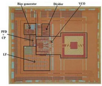
Chip has been fabricated on National Semiconductor 0.18µm five-metal epi-digital CMOS process. Figure 9 shows the die-photo of the chip. The chip core area is 0.75×0.65mm2and power consumption is 7.95mW from 1.8V supply.
The measured VCO frequency is found to be lower than the simulated value by about 180MHz due to the underestimation of parasitic capacitance in simulation and the variation of inductance. This frequency variation has been adjusted to the desired value with the help of external controlled SCA. For all close-loop measurements the input reference signal was set at 5MHz from signal generator. To verify the functionality of the frequency synthesizer, the division ratio was kept at 489 and the measured output frequency was 2.445GHz. Then the division ratio was changed from 480 to 496 with step of unity and the corresponding measured output frequency varied from 2.4GHz to 2.48GHz with resolution of 5MHz. The measured phase-noise performance of the syn-thesizer is shown in figure 10. Measured out-of-band phase-noise is−81.55dBc/Hz and −108.55dBc/Hz at 100kHz and 1MHz offset, respectively. The out-of-band phase-noise is mainly contributed by the phase-noise of VCO. The in-band phase-noise is around−70.30dBc/Hz at 1kHz offset. The possible main reason of such high in-band phase-noise is the phase-noise of the signal gen-erator. With a better input reference signal, either from a crystal or from a signal generator followed by a frequency divider, the in-band phase-noise could be significantly improved.
Figure 10. Measured phase-noise of the synthesizer
From the output spectrum shown in figure 11, the observed reference spur is −40.84dBc at 10MHz (2nd harmonic of the reference) offset from the carrier. This spur can not be predicted. The possible reasons of the spur are i) the charge pump up and down current mismatch, which results in the modulation of dc voltage driving the VCO by a signal of 5MHz and its harmonics; ii) the use of same supply voltage for the VCO and the digital blocks (PFD, digital parts of divider) those run
Figure 11. Measured output spectrum of the synthesizer
at 5MHz or multiple of 5MHz signals, which gives VCO frequency variation for its supply sensitivity and iii)the coupling due to short separation in dense layout between the circuits that are clocked by the reference frequency and the VCO.
Loop bandwidth estimated from the phase-noise plot (figure 10) is around 30kHz, which is less than the design value of 100kHz. The possible reasons of this bandwidth variation are i) the model used for simulation does not include the voltage dependency of the accumulation ca-pacitors, those are used for loop filter implementation for their lower area, which results the variation of loop filter capacitances and ii) the loop filter resistances variation. Measured settling time is less than 25µs for an output frequency change of 75MHz from 2.4GHz. All measured silicon results are summarized in table II.
TABLE II.
MEASURED PERFORMANCE SUMMARY
Supply 1.8V
Process 0.18µmepi-digital CMOS
Architecture Integer-N
Power consumption 7.95mW
Frequency range 2.4 - 2.48GHz
Reference frequency 5MHz
Channel spacing 5MHz
Phase-noise −−81108.55dBc/Hzat 100kHz; .55dBc/Hzat 1MHz Reference spur −40.84dBc
Settling time <25µs
Size 0.4875mm2
Division ratio 480 - 496
On-chip loop filter Yes
VII. CONCLUSION
has also been discussed. This helps to reduce KV CO. The design has been carried out with lowKV CO, which reduces the contribution of noise from phase frequency detector, charge pump, loop filter and input reference frequency source at frequency synthesizer output. In spite of using epi-digital CMOS process, the power consump-tion of frequency synthesizer has been significantly im-proved with acceptable phase noise and reference spur performances. Low silicon area reduces the cost of im-plementation. Also the settling time is quite low, which improves the synchronization time in transceivers. This design is favourable in low-power, low-cost transceiver design. Power consumption can be further reduced by decreasing supply voltage and using high Q inductor which would also reduce phase-noise.
ACKNOWLEDGMENT
Authors are thankful to National Semiconductor for offering its fabrication facilities; Electronics Research Laboratory, Delft University of Technology for using its test equipments and Advanced VLSI Design Laboratory, IIT Kharagpur for its facilities. Also thanks to Ashudeb Dutta and Prabir Saha for their help.
REFERENCES
[1] A. Ajjikuttira, C. Leung, E.-S. Khoo, M. Choke, R. Singh, T.-H. Teo, B.-C. Cheong, J.-H. See, H.-S. Yap, P.-B. Leong, C.-T. Law, M. Itoh, A. Yoshida, Y. Yoshida, A. Tamura and H. Nakamura, “A Fully-Integrated CMOS RFIC for Bluetooth Applications,” inSolid-State Circuits Conference, 2001. Digest of Technical Papers. ISSCC. 2001 IEEE International, 2001, pp. 198–199.
[2] A. Yamagishi, M. Ugajin and T. Tsukahara, “A 1-V 2.4-GHz PLL Synthesizer with a Fully Differential Prescaler and a Low-Off-Leakage Charge Pump,” in Microwave Symposium Digest, 2003 IEEE MTT-S International, June 2003, pp. 733–736.
[3] T.-C. Lee and B. Razavi, “A Stabilization Technique for Phase-Locked Frequency Synthesizers,” Solid-State Cir-cuits, IEEE Journal of, vol. 38, pp. 888–894, June 2003. [4] B. Zhang, P. E. Allen and J. M. Huard, “A Fast Switching
PLL Frequency Synthesizer With an On-Chip Passive Discrete-Time Loop Filter in0.25−µmCMOS,” Solid-State Circuits, IEEE Journal of, vol. 38, pp. 855–865, June 2003.
[5] C.-Y. Wu, C.-Y. Hsieh and W.-M. Chen, “A 1-V 2.4-GHz CMOS FREQUENCY SYNTHESlZER WITH CURRENT-MATCH CHARGE PUMP,” inThe 2004 IEEE Asia-Pacific Conference on Circuits and Systems, Dec. 2004, pp. 433–436.
[6] Y. D. Lei, “A low power CMOS 2.4GHz monolithic integer-N synthesizer for wireless sensor,” inIEEE Inter-national Workshop on Radio-Frequency Integration Tech-nology, Nov. 2005, pp. 219–222.
[7] F. Wang, J. Zhang, X. Wang, J. Lai and C. Sun, “Design of a 2.4-GHz integrated frequency synthesizer,” inDesign Automation Conference, 2005. Proceedings of the ASP-DAC 2005. Asia and South Pacific, vol. 2, Jan. 2005, pp. D/21–D/22.
[8] S. Shin, K. Lee and S.-M. Kang, “3.48mW 2.4GHz range Frequency Synthesizer Architecture with Two-Point Channel Control for Fast Settling Performance,” in SOC Conference, 2005. Proceedings. IEEE International, Sept. 2005.
[9] A. Hajimiri and T. H. Lee, “A general theory of phase noise in electrical oscillators,” Solid-State Circuits, IEEE Journal of, vol. 33, pp. 179–194, Feb. 1998.
[10] J. Mira, T. Divel, S. Ramet, J.-B. Begueret and Y. Deval, “Distributed MOS varactor biasing for VCO gain equaliza-tion in 0.13µm CMOS technology,” inProc. 2004 IEEE Radio Frequency Integrated Circuits (RFIC) Symp., June 2004, pp. 131–134.
[11] H. C. Luong and G. C. T. Leung, Low-Voltage CMOS RF Frequency Synthesizers. Cambridge University Press, 2004.
[12] C. S. Vaucher, I. Ferencic, M. Locher, S. Voegeli, U. Sed-vallson and Z. Wang, “A family of low-power truly mod-ular programmable dividers in standard 0.35-µm CMOS technology,”Solid-State Circuits, IEEE Journal of, vol. 35, pp. 1039–1045, July 2000.
[13] A. Shinmyo, M. Hashimoto and H. Onodera, “Design and measurement of 6.4 Gbps 8:1 multiplexer in 0.18µm CMOS process,” in ASP-DAC ’05: Proceedings of the 2005 conference on Asia South Pacific design automation, vol. 36, 2005, pp. 9–10.
[14] B. Razabi, Design of Analog CMOS Integrated Circuits. Tata McGraw-Hill, 2002.
[15] G. Banchi, Phase-Locked Loop Synthesizer Simulation. McGraw-Hill, 2005.
Debashis Mandalis currently pursuing PhD in the department of Electronics and Electrical Communication Engineering, In-dian Institute of Technology Kharagpur, INDIA. He has com-pleted his MS from same institute. He received his Bachelor of Engineering (BE) degree in Electronics and Telecommunication Engineering from the Bengal Engineering College, Shibpur, INDIA in 2002.
He was with Alliance Semiconductor from 2002 to 2004 as a Circuit Design Engineer. His main research interests are in high-speed mixed-signal and analog circuit design, PLL systems, RF circuits and biomedical applications.