Design of High Speed 32 Bit Multiplier Using
Multiplexer Based Full Adder
C.Dhivya1, M.Thiruppathi2, M.Nargeesh Banu3, D.Maheswari4
PG Student [VLSI], Dept. of ECE, Vivekanandha College of Engineering for Women, Tiruchengode, Tamilnadu,
India1
Assistant Professor, Dept. of ECE, Vivekanandha College of Engineering for Women, Tiruchengode, Tamilnadu,
India2
PG Student [VLSI], Dept. of ECE, Vivekanandha College of Engineering for Women, Tiruchengode, Tamilnadu,
India3
PG Student [VLSI], Dept. of ECE, Vivekanandha College of Engineering for Women, Tiruchengode, Tamilnadu,
India4
ABSTRACT Multiplier is an important element in many signal processing systems. It is an area consuming and slowest element, its performance will determines the performance of a system itself. So that it is necessary to design an efficient multiplier in terms of satisfying the important parameters of power, area and speed. There are many researchers have been worked on the design of increasingly more efficient multipliers. They aim at achieving high speed and lower power consumption even while occupying reduced silicon area. This paper presents a new multiplier architecture that will increase the speed performance of the multiplier and also with reduced area. Simulation of 32 bit multiplier is carried out using modelsim SE PLUS 6.5b and synthesis is done using Xilinx tool.
KEY WORDS : MUX, Wallace Multiplier, Full Adder, Half Adder.
I. INTRODUCTION
Nowadays designing a multiplier with satisfying all the parameters of area, power and speed is a challenging one. Many researches has been made to obtain an efficient multiplier, but still there is a draw backs. Multiplier will plays a major role in Digital signal processing, VLSI signal processing etc[1]. Many of the DSP applications such as mobile phones, MP3 player, digital video recorder, and so on is mainly intensive and it test the limits of their battery life. In many of the signal processing applications, rounded product is needed, because the word size will increase. To avoid this problem a multiplier is to be designed with less area. Nowadays peoples are not interested in slow process products because it is not effective and also not comfortable to use. If the latency will reduced i.e., the amount of delay will be reduced then automatically the speed will gets increased. The designer wants to design a multiplier with rectifying all these problems. This paper will give a better trade off between these parameters.
The Wallace multiplier is basically performed under three stages. They are partial product generation, partial product reduction and partial product addition. In the new multiplier architecture the carry select adder (CSA) is used for the final addition stage, the 4:1 multiplexer is replaced with 8:1 multiplexer to improve the speed performance of the multiplier. The proposed architecture will give better performance than the previous method.
II. RELATED WORK
decrease in delay than the conventional CMOS architecture, along with 11.6% of reduced power consumption realization at 50MHz. The simulations have been carried out using the Xilinx ISE tool. In [2] authors used a new method for parallel multiplication which computes the products of two n-bit numbers by summing only the most significant columns with a variable correction method. It also presents a comparative study of Field Programmable Gate Array (FPGA) implementation of 8X8 standard and truncated multipliers using Very High Speed Integrated Circuit Hardware Description Language (VHDL). Truncated multipliers can be used in finite impulse response (FIR) and discrete cosine transforms (DCT). The truncated multiplier shows much more reduction in device utilization as compared to standard multiplier. Significant reduction in FPGA resources, delay, and power can be achieved using truncated multipliers instead of standard parallel multipliers when the full precision of the standard multiplier is not required. In [3] author presents a comparative study of Field Programmable Gate Array (FPGA) implementation of standard and truncated multipliers using Very High Speed Integrated Circuit Hardware Description Language (VHDL). Truncated multiplier is a good candidate for digital signal processing (DSP) applications such as finite impulse response (FIR) and discrete cosine transform (DCT) etc. Significant reduction in FPGA resources, delay, and power can be achieved using truncated multipliers instead of standard parallel multipliers when the full precision of the standard multiplier is not required. In [5] author produces the comparison of 32x32-bit variants indicate that the Wallace scheme is well suited for high-speed applications, independent of area constraints, while the Dadda and Reduced Area designs deliver best speed when synthesized to minimize area or logic usage.
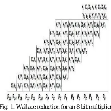
III. WALLACE TREE MULTIPLIER
A Wallace tree is an efficient hardware implementation of a digital circuit that multiplies two integers, devised by Australian Computer Scientist Chris Wallace in 1964.
The Wallace tree has three steps:
Multiply (that is - AND) each bit of one of the arguments, by each bit of the other, yielding results. Depending on position of the multiplied bits, the wires carry different weights.
Reduce the number of partial products to two by layers of full and half adders.
Group the wires in two numbers, and add them with a conventional adder.
Fig. 1. Wallace reduction for an 8 bit multiplier.
The second phase works as follows. As long as there are three or more wires with the same weight add a following layer:
Take any three wires with the same weights and input them into a full adder. The result will be an output wire of the same weight and an output wire with a higher weight for each three input wires.
Fig 1 shows the Wallace tree reduction for an 8 bit multiplier. The benefit of Wallace tree is that there are only
reduction layers shown in Fig 1. Each layer has propagation delay. As making the partial products
is and the final addition is , the multiplication is only , not much slower than addition
(however, much more expensive in the gate count). Naively adding partial products with regular adders would require
time. These computations only consider gate delays and don't deal with wire delays, which can also be very substantial.
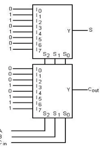
IV. IMPLEMENTATION OF FULL ADDER USING 8:1 MUX
Thefull adder used in the carry select adder is replaced with 8:1 MUX based full adder in order to get the high speed performance when comparing with the existing method. The logic diagram of the full adder using 8:1 MUX is shown in fig 2.
Fig. 2. Logic diagram of full adder using 8:1 MUX
In 8:1 multiplexer there are 8 input ports and one output port. There are also 3 digital inputs that select one of the 8 input port signals to be sent to the output, the particular one selected depending on the binary code at the 3 select inputs. reproduce the inputs as new binary output signals) and analog forms (that are made of analog switches that simply connect one of the inputs to the output). In the Wallace architecture this MUX concept is implemented, the multiplier will becomes modified MUX based multiplier, this will increase the speed performance of the multiplier.
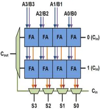
V. CARRY SELECT ADDER
The carry-select adder generally consists of two ripple carry adders and a multiplexer. Adding two n-bit numbers with a carry-select adder is done with two adders (therefore two ripple carry adders) in order to perform the calculation twice, one time with the assumption of the carry being zero and the other assuming one[8]. After the two results are calculated, the correct sum, as well as the correct carry, is then selected with the multiplexer once the correct carry is known.
Fig. 3. Basic building blocks of carry select adder
Fig 3 is the basic building block of a carry-select adder, where the block size is 4. Two 4-bit ripple carry adders are multiplexed together, where the resulting carry and sum bits are selected by the carry-in. Since one ripple carry adder assumes a carry-in of 0, and the other assumes a carry-in of 1, selecting which adder had the correct assumption via the actual carry-in yields the desired result. The number of full adders used in the carry select adder(CSA) is replaced by using 5:2 compressor.
VI. SIMULATION RESULT
Fig. 4. Simulation result of the 32 bit multiplier
VII. RESULT ANALYSIS
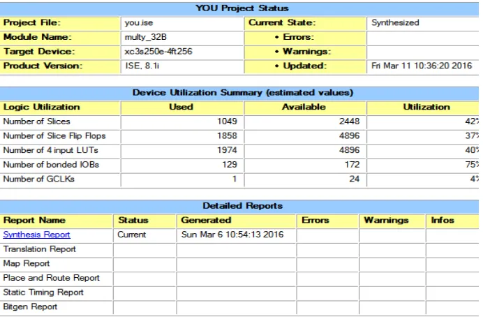
The following table shows the result analysis of the above simulation result. In this the important parameters has been analyzed. The total number of slices used will be 1049, the number of flip flops used will be 1858, the look up tables used will be 1974 and the number of bonded IOBs will be 129.The number of GCLKs will be 1 out of 24. The total utilization will be 47%.
VIII. CONCLUSION AND FUTURE WORK
The simulation and synthesis of multiplier is done in Modelsim SE PLUS 6.5b and functionally tested with different test cases. The combinational path delay is 14.263 ns and Total memory usage is 228900 kilobytes. The results prove that the new architecture is more efficient than the existing one in terms of delay. This approach may be well suited for multiplication of numbers with more than 32 bit size for high speed applications. The power of the proposed multiplier can be explored to implement high performance multiplier in VLSI applications. Wallace tree multiplier using booth algorithm is very good technique for high speed applications. The result shows that the proposed multiplier architecture gives better performance in terms of speed. Further it can be extended up to 64 bit.
REFERENCES
1. Dakupati. Ravi Shankar and Shaik Ashraf Ali, “Design of Wallace Tree Multiplier by Sklansky Adder. International Journal of
EngineeringResearch and Applications (IJERA) ISSN: 2248- 9622 www.ijera.com .Vol. 3, Issue 1, pp.1036-1040, 2013.
2. Suresh R.Rijal, Ms.Sharda and G. Mungale, “Design and Implementation of 8X8 Truncated Multiplier on FPGA”. International Journal of
Scientific and Research Publications, Volume 3, Issue 3, ISSN 2250-3153, 2013.
3. Rais, M.H., “ FPGA design and implementation of fixed width standard and truncated 6×6-bitmultipliers” : Proceedings of the 4th IEEE
International Design and Test Workshop, Nov. 15-17, IEEE Xplore Press, Riyadh, Saudi Arabia, and pp: 1- 4.DOI:10.1109/IDT.2009.5404081, 2009.
4. S.Rajaram, Mrs.K.Vanithamani,“Improvement of Wallace multipliers using Parallel prefix adders” Proceedings of 2011 International
Conference on Signal Processing, Communication, Computing and Networking Technologies (ICSCCN 2011).
5. Chris Y.H. Lee, Lo Hai Hiung, Sean W.F. Lee, nor Hisham Hamid, “A Performance Comparison Study on Multiplier Designs”, Department of
Electrical and Electronic Engineering Universiti Teknologi PETRONAS, Bandar Seri Iskandar.
6. Tronoh, Perak Darul Ridzuan, MalaysiaB.Ramkumar, Harish M Kittur, P.Mahesh Kannan, “ASIC Implementation of Modified Faster Carry
Save Adder”, European Journal of Scientific Research, ISSN 1450-216X Vol.42 No.1, pp.53-58, 2010.
7. Ron S. Waters and Earl E. Swartzlander, “A Reduced Complexity Wallace Multiplier Reduction. IEEE Transactions On Computers, Vo59, No.
8, Published by the IEEE Computer Society, 2010.
8. W.J. Townsend, E.E. Swartzlander Jr., and J.A. Abraham, “A Comparison of Dadda and Wallace Multiplier Delays,” Proc. SPIE, Advanced