A Topology for Equal Power Sharing In a Multiple Input DC-DC Converter for Hybrid Energy System
Full text
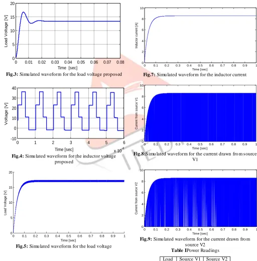
Figure
Related documents
They concluded that supplier selection criteria would continue to change based on an expanded definition of excellence to include traditional aspects of performance (quality,
(2019) Modeling the impacts of urbanization and open water surface on heavy convective rainfall: a case study over the emerging Xiong'an city, China.. Journal
This article summarizes the long-term investigations of Zaporizhzhya, Khmelnitska, and Kalinin NPPs that are located in different geological environments. The
[email protected] &Tech.Nagpur, [email protected].. This increases the Q-factor, allowing greater power to be mediated. In other words, the coil Q
Overall, these results proved that novel MSCs aptamer HM69 is a useful tool for MSCs recognition, capture and enrichment, and HM69-based nanoparticle NAB is a novel potential
The poor treatment efficacy and lack of tailored treatments in depression (part I) underlines the urgent need for an evidence- based approach to select the best
The aim of this study was to assess the accuracy of first trimester fms-like tyro- sine kinase-1 (sFlt-1) and placental growth factor (PlGF), both alone and in combination, in
These platforms work well on cluster systems to meet the requirements of big data applications for smart sustainable cities; entail scalable, evolvable, optimizable, and
