Optimization of electrode geometry and piezoelectric layer thickness of a
de-formable mirror
Alexey V. Kruchenko1,2, Kateˇrina Nováková1,2, and Pavel Mokrý1,2a
1Research Centre for Special Optics and Optoelectronic Systems (TOPTEC), Institute of Plasma Physics, Academy of Sciences
of the Czech Republic, Sobotecká 1660, Turnov, CZ-51101, Czech Republic
2Institute of Mechatronics and Technical Engineering, Technical University of Liberec, Studentská 2, Liberec, CZ-46117, Czech
Republic
Abstract. Deformable mirrors are the most commonly used wavefront correctors in adaptive optics systems. Nowadays, many applications of adaptive optics to astronomical telescopes, high power laser systems, and similar fast response optical devices require large diameter deformable mirrors with a fast response time and high actuator stroke. In order to satisfy such requirements, deformable mirrors based on piezoelectric layer composite structures have become a subject of intense scientific research during last two decades. In this paper, we present an optimization of several geometric parameters of a deformable mirror that consists of a nickel reflective layer deposited on top of a thin lead zirconate titanate (PZT) piezoelectric disk. Honeycomb structure of gold electrodes is deposited on the bottom of the PZT layer. The analysis of the optimal thickness ratio between the PZT and nickel layers is performed to get the maximum actuator stroke using the finite element
method. The effect of inter-electrode distance on the actuator stroke and influence function is investigated.
Applicability and manufacturing issues are discussed.
1 Introduction
In the middle of the last century, the resolution of terres-trial astronomical telescopes reached such limits that fur-ther improvement of their resolution required a develop-ment of methods for the correction of atmospheric distor-tions. The first concept of so called adaptive optics was envisioned by Babcock [1] in 1953, who proposed to use a deformable mirror to correct the atmospheric seeing. It took more than forty years to achieve a technological level that would allow the construction of adaptive optics.
During the last few decades, several concepts of de-formable mirrors were implemented [2]. Examples to be mentioned here are (i) segmented mirrors, (ii) continuous thin plate mirrors, (iii) monolithic mirrors, and (iv) mem-brane or pellicle mirrors. It is the continuous thin plate type of mirrors, which has become a very popular structure mainly due to their lower technological difficulty. While an array of discrete actuators can always be adjusted to produce zero mean figure error, there is a residual ripple which causes an rms surface error, the magnitude of which can be reduced by closer spacing of actuators. Unfortu-nately, requirement of dense spacing of the actuators can be satisfied in small and medium size mirrors with many difficulties.
With the onset of real-time wavefront corrections [3], a very convenient type of electromechanical transducers that is used as a actuator in deformable mirrors is the
piezo-ae-mail: [email protected]
electric actuator. The greatest advantage of piezoelectric actuators is their fast response and relatively simple con-struction. In order to increase the number of degrees of freedom, deformable mirrors based on piezoelectric uni-morphs or biuni-morphs have become a very popular and in-tensively studied concept [4–8].
Generally, this type of the deformable mirror consists of a layered sandwich composite structure, where the re-flective layer is bonded on a piezoelectric layer. The reflec-tive layer is usually made of a conducreflec-tive metallic material and forms an equipotential surface. On the opposite side of the piezoelectric layer a system of electrodes is deposited using conventional techniques such as lithographic sput-tering. By applying a voltage to a particular electrode, the piezoelectric layer is deformed due to the inverse piezo-electric effect in the in-plane directions. This produces bending moments in the reflective layer of the particular segment of a deformable mirror and yield its out-of-plane deformation (see Fig.1).
The necessity of large voltage-induced deformations is a reason for the use of piezoelectric ceramics as piezo-electric layers. These ceramics are based on a ferroelec-tric perovskite materials, such as lead zirconate titanate (PZT). Large piezoelectric response of PZT ceramics is achieved due to extrinsic contributions to piezoelectric co-efficients due to movements of domain walls in an applied electric field. Since the movements of domain walls are irreversible in high electric fields, the characteristic fea-ture of the actuation is a pronounced hysteresis [8]. This © Owned by the authors, published by EDP Sciences, 2013
wavefront
wavefront
deformable
mirror
reflective layer
active layer
Figure 1. Incoming wavefront, which is distorted by atmo-spheric turbulence, is reflected from a deformable mirror, which corrects the shape of the wavefront to be planar again. In this work the deformable mirror is designed as a composite structure, where the reflective layer is bonded on the active piezoelectric layer.
strongly hysteretic response represents a source of diffi -culties in the control of particular deformable mirror seg-ments position. It is clear that reduction or complete elim-ination of hysteresis would greatly ease the robustness of control algorithms.
There exist two possibilities to reduce hysteresis in the electromechanical response: (i) to use the non-hysteretic piezoelectric material such as electrostrictive or magne-tostrictive materials [9], (ii) to reduce the applied elec-tric field to the piezoelecelec-tric material while keeping the reasonable piezoelectric response of the whole composite structure.
Aforementioned issues have motivated the work pre-sented below, where we will address the problem of the optimization of the composite structure of the deformable mirror to achieve the maximum out-of-plane deflections at minimum applied voltages to the piezoelectric structure using finite element method (FEM) numerical simulations. In Sec.2, we will show the geometry of the deformable mirror. Further detail of the FEM model will be presented in Sec.3. In Sec.4, we will present the results of our nu-merical simulation and their discussion. Conclusions will be presented in Sec.5.
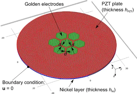
2 Geometry of the deformable mirror
Geometry of the deformable mirror is presented in Fig.2. The deformable mirror consists of a double-layer sand-wich composite structure. In our study, the reflective layer of thicknesshNi is made of nickel. The reflective nickel layer is bonded on a piezoelectric layer of thicknesshPZT made of a PZT-2. The reflective layer forms an equipoten-tial at the bottom surface of the piezoelectric layer.
On the top surface of the piezoelectric layer, a system of honeycomb golden electrodes is deposited using litho-graphic sputtering. The distance between the sputtered
Figure 2. Geometry of the finite element method (FEM) model of the deformable mirror. It consists of the nickel reflective layer
of the thicknesshNiand of the PZT layer of the thicknesshPZT.
Honeycomb structure of gold electrodes is deposited on the bot-tom of the PZT layer. Nickel layer itself can be considered as a grounding electrode. The mirror is fixed in its edges which indi-cates the boundary condition of zero displacement on this edge,
i.e.u=0.
electrodes is denoted by a symbold. It is considered that arbitrary external voltage can be applied at each particular electrode. It is considered that the deformable mirror is fixed in a rigid frame along its circumference.
3 FEM model of the deformable mirror
The basic equation which rules the analysis is the formula for mechanical stress distribution:
− ∇ ·T=0, (1)
whereTis mechanical stress tensor. Second, we consider the Maxwell equation for the zero flow of electric displace-ment inside the composite body,
∇ ·D=0, (2)
whereDis electric displacement vector. Electric fieldEis given by
E=−∇V, (3)
whereV is the electric potential. Third, for the isotropic non-piezoelectric material (i.e. nickel), there are given constitutive equations expressed by the Hooke’s law,
S= 1
YT−
ν
Y(T
TI−T), (4)
whereY andνare Young’s modulus and Poisson’s ratio of an isotropic material, respectively. The symbolIstands for the second-order identity matrix and S is the elastic strain tensor coupled with the displacement vector u by the formula:
S= 1 2[(∇u)
T+∇u]. (5)
In the non-piezoelectric material, the electric displace-ment is considered as a linear function of the electric field:
0.9 1.0 2.1 2.8 3.3 3.7 4.4 5.3 (10-2 µm) x
y
(a)
(b)
x y
z
(c)
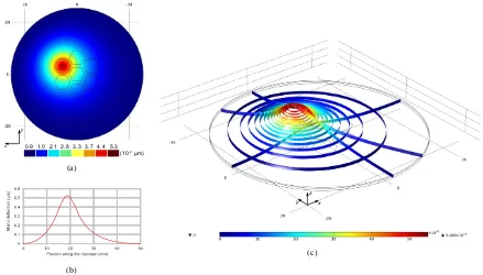
Figure 3. Graphical presentation of the deformable mirror displacement. One off-centered honeycomb electrode is connected to the electric potential of 200 V, the remaining electrodes are short circuited. The surface boundary between the PZT and nickel layer is taken
as a grounding electrode. (a) The 2D surface plot in the plane (xy) of the displacement of the mirror; (b) plot along the line which goes
along the diameter of the mirror through the all three honeycomb electrodes; (c) the 3D graphical interpretation of the displacement of the mirror, it is shown using the iso-surfaces and slices. In any case, the color legends mean the mechanical displacement value. The
given parameters ared=1 mm,R=3 mm,hPZT=0.5 mm, and the nickel layer thicknesshNi=0.18 mm.
whereris the relative permittivity of the material. Forth, for the piezoelectric material, the constitutive equations are given by the state equations for the piezoelectric mate-rial, written in a following form:
D=[T]E+[d]T
S=[d]E+[sE]T, (7)
where [sE] are elastic coefficients matrix for constant elec-tric field, [d] is piezoelectric coefficients matrix and [T] is dielectric permittivity matrix at constant mechanical stress.
The mechanical boundary condition, the displacement at the edges of the mirror, is considered as the fixed one, i.e.u=0.
4 Results and discussion
Figure3shows the example of the FEM numerical simula-tion of the deformable mirror. In the resented simulasimula-tion, the off-centered honeycomb electrode is connected to the electric potential of 200 V, the remaining electrodes are short circuited. The following material parameters were considered: d = 1 mm, R = 3 mm, hPZT = 0.5 mm, and the nickel layer thickness hNi = 0.18 mm. By ap-plying the FEM model presented in the previous Section, displacements of the deformable mirror were calculated and presented. Figure 3(a) presents the 2D surface plot in the plane (xy) of the displacement of the mirror. Fig-ure3(b) presents the plot along the line which goes along
the diameter of the mirror through the all three honeycomb electrodes. Figure3(c) shows the 3D graphical interpreta-tion of the displacement of the mirror, it is shown using the iso-surfaces and slices.
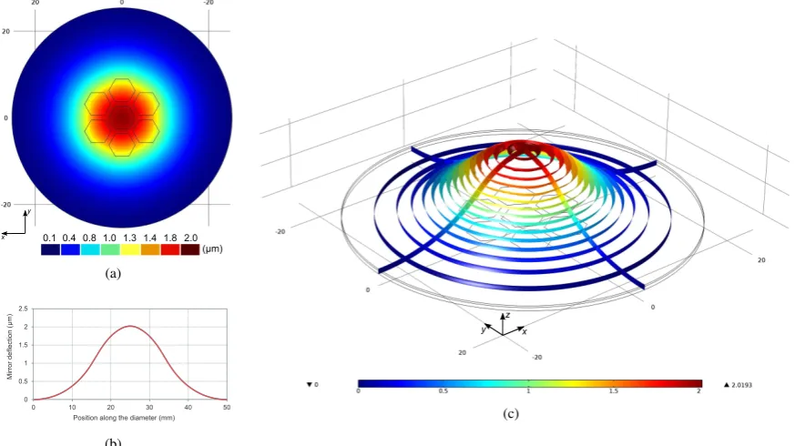
Figure4presents results of a similar FEM simulation, however with all honeycomb electrodes connected to the electric potential of 200 V. The remaining numerical pa-rameters are the same as those in Fig. 3. The maximal value of the mirror deflection which could be achieved is 2.02µm.
In order to find the optimal ratio of the thicknesses of the nickel and PZT layers, a series of numerical FEM ulations has been performed. At the first step of each sim-ulation, the geometry of the FEM model was modified and the thicknesses of the nickel and PZT layers were set to particular values. In the second step, the displacement of the deformable mirror was calculated. In the third step, the value of the maximum deflection above the activated electrode was determined.
0.1 0.4 0.8 1.0 1.3 1.4 1.8 2.0 (µm) x
y
(a)
(b)
x y
z
(c)
Figure 4. Graphical presentation of the deformable mirror displacement. All honeycomb electrodes are connected to the electric potential of 200 V. The surface boundary between the PZT and nickel layer is taken as a grounding electrode. (a) The 2D surface plot
in the plane (xy) of the displacement of the mirror; (b) plot along the line which goes along the diameter of the mirror through the all
three honeycomb electrodes; (c) the 3D graphical interpretation of the displacement of the mirror, it is shown using the iso-surfaces and
slices. The remaining numerical parameters are the same as those in Fig.3. The maximal value of the mirror deflection which could be
achieved is 2.02µm.
Figure 5. Dependences of the maximal values of the
mir-ror deflection as a function of the nickel layer thickness hNi
(0.02−0.6 mm). The parameter of each curve is the PZT layer
thicknesshPZT(0.2−0.8 mm). All the combinations of the
dif-ferent thicknesses of the PZT and nickel layer were used for the finite element method (FEM) model. It can be seen that the thiner layers of both nickel and PZT are the larger displacement of the mirror can be achieved.
Figure 6 presents thickness of the nickel, which re-sults in the maximum deflection of the deformable mirror, versus the thickness of the PZT layer. The dashed line presents the fit of the optimal nickel and PZT thicknesses to the linear dependence obtained by the method of least squares (i.e. the linear regression).
y = 0.375x - 0.002
0 0.05 0.1 0.15 0.2 0.25 0.3 0.35 0.4
0.15 0.25 0.35 0.45 0.55 0.65 0.75 0.85
Ni
c
k
e
l
la
y
e
r
th
ic
k
n
e
s
s
hN
i
(m
m
)
PZT layer thickness hPZT(mm) Linear regression
Figure 6. Linear regression of optimal values of the thicknesses of the nickel and PZT layers. The decisive values for the op-timization were the maximal values of the mirror displacement
which could be seen in Fig.5. It is shown that for the certain
value of the PZT layer thickness could be used certain range of the nickel layer thicknesses, particularly for thicker PZT layers
(from 0.65 mm).
Figure 7.Dependences of the maximal values of the mirror
de-flection on the honeycomb electrode distanced(0−3 mm). The
parameter of the curves is the lengthR(2.5−3 mm) of the edge
of the regular hexagon electrode. All the combinations of the
different electrode distances and edge lengths were used for the
finite element method (FEM) model. There is a visible maxi-mum in the range of values for the distance between electrodes,
(0.5−1 mm). Also, the almost linear dependence on the
param-eterRcould be seen, i.e. the bigger surface of each electrode the
bigger deflection of the mirror.
1.72 1.73 1.74 1.75 1.76 1.77 1.78 1.79 0 .4 0 .4 2 5 0 .4 5 0 .4 7 5 0 .5 0 .5 2 5 0 .5 5 0 .5 7 5 0 .6 0 .6 2 5 0 .6 5 0 .6 7 5 0 .7 0 .7 2 5 0 .7 5 0 .7 7 5 0 .8 0 .8 2 5 0 .8 5 0 .8 7 5 0 .9 0 .9 2 5 0 .9 5 0 .9 7 5 1 M ax im al m ir ro r de fl ec ti on (µ m )
Hexagonal electrodes distance d (mm)
R=2.5 mm
Figure 8.Detailed study of the dependence of the maximal val-ues of the mirror deflection on the honeycomb electrode distance
d. Very small step of 0.025 mm was taken into the simulations.
The analysis is performed just for the hexagonal electrode edge
R = 2.5 mm. The optimal distance between the electrodes is
betweend=0.675 mm andd=0.925 mm.
the bigger surface of each electrode the bigger deflection of the mirror.
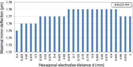
Detailed study of the dependence of the maximal val-ues of the mirror deflection on the honeycomb electrode distance d is presented in Fig. 8. Very small step of 0.025 mm was taken into the simulations. The analy-sis is performed just for the hexagonal electrode edge
R=2.5 mm. The optimal distance between the electrodes is betweend=0.675 mm andd=0.925 mm.
5 Conclusions
FEM model of a deformable mirror, which consists of a double-layer composite structure, was developed. The double-layer composite structure consists of a reflective nickel and a active PZT materials. A series of FEM simu-lations were performed, in order to find optimal thickness ratio of the reflective and active layers. The effect in inter-electrode distances on the maximum deflection of the de-formable mirror was analyzed.
The obtained results provide an efficient and simple tool for the design of deformable mirrors with piezoelec-tric materials. The optimal thickness ratio of the double-layer composite structure would result in a deformable mirror with minimal hysteresis in the electromechanical response. Such a system allows the use of effortless con-trol algorithms.
Aknowledgments
This work was supported by the European Regional De-velopment Fund and the Ministry of Education, Youth and Sports of the Czech Republic in the Project No. CZ.1.05/2.1.00/03.0079: Research Center for Special Op-tics and Optoelectronic Systems (TOPTEC), by the Stu-dent Grant SGS 2012/7821 Interactive Mechatronics Sys-tems Using the Cybernetics Principles, and by the Project TA01010878 of Technology Agency of the Czech Repub-lic.
References
[1] H.W. Babcock, Publ. Astron. Soc. Pac.65, 229 (1953) [2] J. Hardy, Proceedings of the IEEE66, 651 (1978) [3] F. Merkle, Real-time Wave-front Sensing And
Adap-tive Optics, inDiffraction-limited Imaging With Very
Large Telescopes, edited by Aalloin, Dm and Mariotti,
Jm (Nato, Div Sci Affairs; Minist Affaires Etrangeres France; Natl Sci Fdn; Cnrs; European Space Agcy, 1989), Vol. 274 ofNato Advanced Science Institutes
Series, Series C, Mathematical And Physical Sciences,
pp. 237–248, ISBN 0-7923-0192-7, Nato Advanced Study Inst On Diffraction-limited Imaging With Very Large Telescopes, Cargese, France, Sep 13-23, 1988 [4] H. Zhao, P. Fekete, J. OByrne,Prototype bimorph
mir-ror for the AAT adaptive optics system, inAdaptive
Optics And Applications, edited by Tyson, RK and
Fugate, RQ (Soc Photo Opt Instrumentat Engineers, 1997), Vol. 3126 of Proceedings Of The Society Of
Photo-optical Instrumentation Engineers (SPIE), pp.
384–390, ISBN 0-8194-2548-6, Conference on Adap-tive Optics and Applications, SAN DIEGO, CA, JUL 30-AUG 01, 1997
[5] M. Huonker, G. Waibel, A. Giesen, H. Hugel, Fast
and compact adaptive mirror, inLasers in material
processing, edited by Beckmann, LHJ (European Opt
Soc; Soc Photo Opt Instrumentat Engineers; Commiss European Communities, Directorate Gen Sci Res & Dev, 1997), Vol. 3097 ofProceedings of the society of
photo-optical instrumentation engineers (SPIE), pp.
310–319, ISBN 0-8194-2517-6, Conference on Lasers in Material Processing, MUNICH, GERMANY, JUN 16-20, 1997
[6] R. Signorato, O. Hignette, J. Goulon, Journal of Syn-chrotron Radiation5, 797 (1998)
[7] E. Yang, K. Shcheglov,A piezoelectric unimorph de-formable mirror concept by wafer transfer for ultra
large space telescopes, in Adaptive Optical System
ceedings Of The Society Of Photo-optical
Instrumen-tation Engineers (SPIE), pp. 703–710, ISBN
0-8194-4618-1, ISSN 0277-786X, Conference on Adaptive Optical System Technologies II, WAIKOLOA, HI, AUG 22-26, 2002
Topics in Quantum Electronics, IEEE Journal of 13, 155 (2007)