REDUCED ORDER LINEAR QUADRATIC REGULATOR
PLUS PROPORTIONAL DOUBLE INTEGRAL BASED
CONTROLLER FOR A POSITIVE OUTPUT ELEMENTARY
SUPER LIFT LUO-CONVERTER
1 N.ARUNKUMAR, 2 T.S. SIVAKUMARAN, 3 K.RAMASH KUMAR, 4 S.SARANYA
1
Department of Electrical and Electronic Engineering, TRP Engineering College (SRM group), Trichy, Tamilnadu, India.
2
Department of Electrical and Electronic Engineering, Arunai Engineering College, Thiruvanamalai, India.
3, 4
Department of Electrical and Electronic Engineering, Dr. S.J.S. Paul Memorial College of Engineering Technology, Puducherry, India,
E-mail:[email protected] , [email protected] , [email protected] ,
4
ABSTRACT
The design and analysis of reduced-order linear quadratic regulator (ROLQR) plus proportional double integral controller (PDIC) for enhancing the dynamic performance of the positive output elementary super lift Luo-converter (POESLLC) worked in continuous conduction mode (CCM) is carried out, The ultimate aim is designing the PDIC is to obtain the efficient output voltage regulation with zero steady state error. The ROLQR is mainly designed to regulate inductor current which in turn enhances the dynamic performance of the converter. The POESLLC is modeled using state space average technique. Extensive simulation is carried under both line and load variations and the controller platform are evaluated using well as in the experimental model (digital dsPIC30F4011controller). The simulation and experimental results are illustrated that the POESLLC with ROLQR plus PDIC tracks reference voltage, regulate the inductor current and robust in spite of line and load variation.
Keyword: DC-DC Power Conversion, Positive Output Elementary Super Lift Luo-Converter, Linear Quadratic Regulator, Proportional Double Integral Controller And State-Space Average
Model.
1. INTRODUCTION
Positive output elementary super lift Luo-Converter (POESLLC) is one of the recent development of dc-dc power converter which fines wider applications in the various medical equipment, LED TV, mobile phones, computer peripheral equipments, data transfer equipments in robot systems, renewable energy power systems, and industrial drives [1-2]. The POESLLC converts the positive dc input source voltage into positive dc load voltage. The POESLLC has several advantages such as increased voltage transfer gain, huge power density, and higher efficiency and suppressed output voltage and inductor current ripples [3-5]. In general, the POESLLC has intricate non-linear model with circuit parameters dissimilarity,
index This quality of LQR has initiated many
researchers to effectively utilize this method in the area of power electronics converters in [13, 14]. The performance indices were chosen by pole placement technique which mainly depends on the accurate placement closed loop poles. This method is disadvantages when compared with LQR which requires larger computations. The cost function is designed from an initial controller by frequency domain approach in method, [15]. The major constraints in the design of control based onfrequency domain is the presence of a zero in the right hand side of the plane in many of the averaged models increasing the value of the inductor current may change the location of the zero to the lower frequency region towards the right side of the plan. This in turn, creates a phase lag which restrains band width for constant operation of the converter Best possible solution can be provided by a LQR which control offers a systematic procedure for the computation of controller parameters leading to robust control. The design and implementation of reduced order SMC plus proportional double integral controller (PDIC) for negative output elementary super lift Luo-Converter has been addressed [16]. But, the output voltage shows overshoots and the settling time of the system is larger during dynamic operating conditions. The reduced order frequency SMC for dc-dc converter has been well presented in [17]. But huge initial start if overshoots and large peak overshoots are evident which is quite undesirable. The current and regulation for parallel dc-dc converter and load voltage control positive output elementary Luo-converter using SMC will full order has been analysis in [18],[19-22]. But the sensors required are of larger in number and at the same time this method involves more computations. And more over the output thus obtained witnesses overshoots during dynamic performs which has to be reduced. In [23]-[24], SMC with (constant switching frequency) PWM has been reported for higher order dc-dc converters. Yet, this control method has more calculations, complex implementation and needs of larger sensors for sensing the circuit feedback variables. These above maintained problems can easily overcome
by design of reduced order linear quadratic regulator (ROLQR) plus PDIC for the POESLL Converter. The ROLQR plus PDIC is designed for POESLL, the state space averaging technique is adapted to derives the reduced order model for POESLLC.Two loop control has been designed for the dc-dc converter in which the inner loop is designed using ROLQR which is mainly used to regulate the inductor current and the outer loop is designed using PDIC which is alternately used for the output voltage regulation.PDIC also reduces the steady state error under line and load variations. The controller coefficient of ROLQR is found with the help of reduced order state space average model of the POESLLC using capacitor charge balance rule method. The PDIC parameters are tuned with the help of Ziegler Nichol’s Tuning method. The major impacts of proposed controller ROLQR along with PDIC for the POESLLC are the realization with variable frequency (with in the boundary limit), arrangements, lesser computation and reduced number of sensing devics.The organization of this paper is as follows. Section 2 presents the circuit operation and state-space average reduced-order modeling of the POESLLC. The systematic step by step design procedure of ROLQR plus PDIC for the POESLLC is presented in section 3. The results of the POESLLC using ROLQR plus PDIC at the various operating regions are discussed in sections 4. The conclusions are listed in section 5.
2. DESIGN AND MODELING OF POESLLC
The POESLLC is depicting in Fig.1 (a) is a new series of dc-dc converter which successfully increases the voltage transfer gain in high rate. In the power circuit, Vin is a dc input supply voltage,
achievable. The working principle of
thisconverter can be explained in two modes viz, the switch ON-mode and OFF-mode. Fig.1 (b) and Fig.1(c) show the two operating interval of the POESLLC [1]. The reduced order state apace averaged model is derived for the converter, since it is an unique method for modeling switching mode converter in which the PWM type converters are switched in between two or more non linear circuits depending upon the duty cycle ratios. In addition to this technique also includes the duty cycle ratios along with independent voltage and currents.The working along with the modeling details can be explained as follows,
(a)
(b)
(c)
Figure.1 Power Circuit Of POESLLC, (A) Topology, (B) Equivalent Circuit During Mode 1 Operation, (C)
Equivalent Circuit During Mode 2 Operation.
During ON time, the switch Q is in ON state, the diode D1conducts. The capacitor C1 is charged to a constant value of a voltage up to a level of Vin in smaller interval of time. The current through the inductor iL1 dependent with Vin. The output capacitor, Co supplies the energy to the load. The equivalent circuit of POESLLC in stage 1 operation is shown in Fig. 1(b). The state space equation can be engraved as (1)
Mode 1: Switch is ON
1 1
di L
L V
in dt
dVo Vo
Co
dt R
=
= −
Switch ON (1)
During off time, the switch in off state the switch Q is in OFF state, diode D2conduct and for this reason, the inductor current decreases with voltage - (Vo - 2Vin) to provide energy to Co and load branch. The equivalent circuit of POESLLC in state 2 is shown in Fig.1(c). The state space equation can be inscribed as (2)
Mode 2: Switch is OFF
1 2
1
1
di L
L Vin Vo dt
dVo Vo
Co i
L
dt R
= −
= −
Switch OFF
(2)
Using the capacitor charge balance rule on C1 , the equation (3) for entire switching time period can be written. Where u is the status of the switch (d=1 when the switch is ON, and d=0 when the
(3)
As there are two capacitor in the POESLLC, which
are VC1 = Vin, Vo, it is only necessitate to chose as a state space variable except Vin. Collectively with inductor current iL1, all state space variables of the POESLLC are chosen for example the inductor current iL1, and voltage vo respectively x1, and x2. Utilizing (1), (2), and (3),
1
1
(1
)
10
C
L
dV
dt
the reduced-order state-space average modeling
of the POESLLC can be reached as expressed by equation (4).
. 1
0 2
1
1 1
. 1 1 1
0
1 [0 1]
d
d i
L L i
L L
V in
d V
o V
o
C RC
o o
i L Y
V o
− −
−
= + −
−
=
(4)
The design details of the converter are as follows: The inductor value must be chosen by assuming appropriate value of ripple current and the load current, ripple current of inductor is 10% to 20% of the average output current is assumed and the inductor value is determined by,
2
1
1
Vo
Vin
iL
L
−
∆
=
(5)
Where
∆
iL
1
is the peak to peak ripple current, L1is the inductor. The capacitor value is determined by assuming the output voltage ripple as 1% to 2% of output voltage. The capacitor value is determined by,
(6)
The following are the parameters designed for the converter Vo, f, L, C & R.
[image:4.595.77.513.65.767.2]The design details of the converter is given below
Table 1: The Designed Specification Of POESLLC CircuitComponents Are Listed Below.
Parameters name Symbol Value
Input Voltage Vin 12V
Output Voltage Vo 36V
Inductor L1 100µH
Capacitors C1, Co 30 µF
Nominal switching frequency
Fs 100kHz
Load resistance R 40Ω -70Ω
Output power Po 25.92W
Input power Pin 28.236W
Average input current Iin 2.353A
Duty cycle various different values according to voltage variation
D 0.3 to
0.7
Efficiency η 91.8%
Average output current Io 0.72 A
Peak to Peak Inductor Current Ripple
∆
iL125% of
Iin
Peak to Peak Capacitor
Ripple
∆
V
o0.12V
The determined values of the inductor and capacitor of POESLLC are
2
(1 ) 100 1
1 (1 )
30
VO Vin
L d T uH
iL V
d o
Co uF
f Vo R
−
= − =
∆
−
= =
∆
(7)
The design specifications are substituted in (7) and after using the phase-variable transformation, A, B, C, and D matrices become
[ ]
0 5000 0
, , [165000000 0], 0 11000 16666.67 1
A= − B= C= D=
−
(8)
3. DEVELOPMENT OF CLOSED LOOP CONTROL METHODS
Figure 2. Development Of POESLLC Using ROLQR Plus PDIC
(1
d Vo
)
Vo
fRC
−
The main motivation of this section is to deal
about the design of controller for POESLLC. The ROLQR plus PDIC scheme for a POESLLC converter is shown in Fig. 2. The controller is divided into two loops namely, an inner current loop which uses ROLQR for regulate the inductor current, and an outer voltage loop applying the PDIC to regulate the output voltage of POESLLC and reduced steady state error. The input to the PDIC is the output voltage error e1 and the output sets the average power loss. The input to the ROSMC is current error e2. The output of ROSMC u is the control signal, which in turn sets the new duty ratio of the switching pulse for driving the power MOSFET switch of the POESLLC.
3.1 Generation Of Reference Current
The reference inductor current of POESLLC is derived by using the equations (8) is
1
loss o L ref
in
P P
i
V
+
= (9)
Where,
P
o=
V I
o o
P
loss=
K e
p 1+
K
i∫∫
e dt
1
e
1=
V
o−
V
oref
In this study, the term Ploss indicates the converter switching and resistive losses. Owing to losses in POESLLC, the output capacitor voltage will fall. When the output capacitor voltage falls down the reference output voltage, the converter cannot be able to follow the reference inductor current closely. Therefore, an appropriate PDIC is applied which control the output capacitor voltage to the reference output voltage level, which is expressed as equation (8). The term Po represents the load power, which is the product load voltage and load current of the converter.
3.2 Design Of Rolqr
The theory of optimal control is troubled with working a dynamic system at minimum cost. The time in varying LQR is utilized as tracking current regulator. In this case, ROLQR controller gain matrix for NOESLLC is evaluated by suitable selection values of R and Q (weight
matrix). The values for Q and R matrices are determined based on system performance
[ ]
2.16
1
,
1
1
1000
Q
=
R
=
(10)Q matrix is preferred in such a way that most weight age is given to inductor current, in order that inductor current of POESLLC is regulated very effectively using ROLQR controller. Q and R could be non-negative semi-definite and positive definite, correspondingly, which are chosen such that the scalar quantity xTQx is all the time positive or zero at every time t for the entire functions x(t), and the scalar quantity uTRu is always positive at each time t for all values of u(t). In terms of eigen values, the eigen values of Q would be positive, whereas those of R could be positive. For a continuous time model the state-feedback control law u = −KF x minimizes the quadratic cost function;
(
(.), (.))
1 ( ) 2f
o t
T T
t
J x u =
∫
x Q x+u R u dt (11)Subject to the system dynamics
.
X
=
AX
+
BU
(12)For the designed model, the quadratic cost function is found after substituting the values of X, Q, R in Equation (11)
2 2 2
1 1 2 2
[(2.16 2 1000 ) ]
f
o
t
t
x + x x+ x +u dt
∫
(13)The control law is determined to be
1 T
F
u
R
−B Kx
u
K x
= −
=
= −
(14)Where, KF is the feedback gain matrix and K is the return function matrix. The unknown coefficients of the return function matrix are found by solving the Ricatti equation.
* * ( * )1 *
K Q A PA A PB R B PB −B PA
= + − + (15)
On solving Eq. (15), the return function matrix K is found to be
1 1 1 2
2 1 2 2
2 . 2 1 1 1 0 0 0
K K
K
K K
= =
On substituting the value of K matrix in the
equation, KF = −R-1BTK the feedback gain matrix KF is obtained. It is found to be
[1 1000]
Therefore, the control law becomes then we
assume u=d,
1 1 2
1( ref ) 1000( ref ref)
u= − x −x − x −x (17)
Once again the equation (16) becomes expressed as (17)
1 1 2 2
( )
u= −K e+K e
Where, K1= 1 and K2= 1000 (18)
3.3 DESIGN OF PDIC
A main role of PDIC is selected here for providing an well as to reduced steady state error and good output voltage regulation for POESLLC. The dc output voltage is sensed and compared with reference output voltage, which gives the error signal. This error signal is processed by the PDIC to maintain the output voltage constant and reduce the steady state error. Here, the PDIC output sets the average reference inductor current for inner current loop through the Ploss, Po and input voltage.The PDIC parameters, proportional gain (Kp) and double integral times
(Tis), are evaluated using Zeigler – Nichols tuning
method. The PDIC parameters, proportional gain (Kp) and double integral times (Tis), are obtained
by using Zeigler–Nichols tuning method [13]-[15]. The transfer function (T.F) model of equation (4) can be expressed as equation (19), with help of MATLAB program commends,
-13 8
2 7
2.274
s + 1.65e
T.F=
s + 666.7 s + 5.5e
(19)Design aspect, the term 2.274e-13s in the numerator of the T.F model is very small and hence it can be neglected. Therefore, the T.F becomes
8
2 7
1.65e
T.F=
s + 666.7 s + 5.5e
Kp
(20)
The characteristics equation with proportional control is expressed by
S2+ 666.7 s + (5.5e7+Kcr 1.65e8) = 0 (21) The routh array of equation (21) is
S2 : 1 (5.5e7+1.65e008 Kcr) S : 666.7 1.389e12 K cr s1 : (-8.333e7+2247116969 Kcr) s0 : 1.389e12 Kcr
From this routh array, the range of K for stability is (-8.333 e7+2247116969 Kcr) > 0, Kcr > 0.037, 0 < Kcr < 0.037. So, the ultimate critical gain Kcr = 0.037, and their corresponding
ω
n=210447 [image:6.595.334.513.399.520.2]rad/sec and Pcr=2*pi
ω
n=2.9856e-5. After the tuning the controller using this method, the POESLLC is providing a sustained oscillation with ultimate gain for stability can be found by Kcr=0.02 and their corresponding ultimate period Pcr=0.0012s. Using this method the values of Kp=Kcr/2=0.01 and integral times Tis=Pcr/.2=0.0011s and 0.000621s (this value is selected based on the system response, trial and error method) are determined.Table 2: performance of the POESLLC
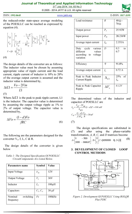
4. SIMULATION RESULTS
The design model and performance of POESLLC is consummate in continuous conduction mode and simulated using MATLAB/simulink.simulation has been carried out using values same as that of the experimental values. The ultimate aim is to achieve a robust two controllers for regulating the output voltage and inductor current in the converter in spite of uncertainty and load disturbances this is proved in the Table 2 the output voltage obtained using this controller settles down at 0.01s with a rise time 0.005s.The converter specifications under consideration are rise time, settling time, maximum peak overshoot, and steady state errors which are shown in the Table 2 No overshoot or undershoots are evident and the error in load variation are much lesser then 5%.The
Specifications ROLQR plus
PDIC controller
Settling time(s) 0.05
Peak overshoot (%) 0
Steady state error(v) 0
Rise Time(s) 0.0060
Output Ripple
0 0.01 0.02 0.03 0.04 0.05 0.06 0.07 0.08 0.09 0.1
0 5 10 15 20 25 30 35 40
Time (Sec )
O
u
tp
u
t
V
o
lt
a
g
e
(
V
)
Vin=15V Vin=12V
Vin=9V
0 0.01 0.02 0.03 0.04 0.05 0.06 0.07 0.08 0.09 0.1 0
5 10 15 20 25 30 35 40
Time (Sec)
O
u
tp
u
t V
o
lta
g
e
(
V
) 50 Ohm
30 Ohm 60 Ohm performance specifications for the POESLLC
with PDIC plus LQR better than the SMC controller in the [16], The results thus obtained with ROLQR plus PDIC are in concurrence with mathematical calculations. The simulation of the POESLLC with ROLQR plus PDIC is also carried out by varying the load not limiting to R load and is given in Table 3. It is shown in Table 3 that controller tracks the reference voltage in spite of load variations. When the load resistance is varied from 40Ω, 50Ω, 60Ω, and70Ω, the ROLQR plus PDIC is efficient enough to track the output voltage as 36.015V, 36.042V, 36.007Vand36V respectively for the reference voltage 36V.Agin when the inductance added to the load resistance of 40 Ω to 70 Ω, the output
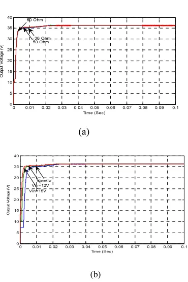
voltage thus obtained 36V constantly. The steady state error is 0.1% and 0.2% respectively. The simulation is also carried out using RLE load with resistance of 70 Ω, inductance of 100µH and an ideal dc voltage source 2V.The response of the converter is performed well all the aspects of load transient there by tracking the voltage as 36V. The simulation is also carried out by varying the input voltage and load resistance and the corresponding, input voltage, output voltage, inductor current, error and load current as shown in Fig respectively. The input voltage is initially set as 12V until 0.01s and then varied from 12V to 9V and again at 0.03s 9V is varied to 12V .From 12V to again change 15V at 0.04s and finally set at 0.05s.The corresponding output response of converter shows fixed output regulation.
Table 3: Output Response For Load Variations
R (Ω)
L (µH)
C
(µF) E (V)
Referen ce voltage
(V)
Output Voltag
e (V)
40 30 5 - 36 36.015
50 50 10 - 36 36.042
60 75 15 - 36 36.007
70 100 30 2 36 36.000
Table 4: Output Response With Variable Components
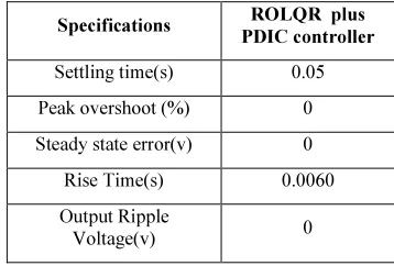
4.1 Start-Up Transient
(a)
[image:7.595.307.514.97.643.2](b)
Figure 3. Simulated Startup Response Of Output Voltage Of POESLLC Using ROLQR Plus PDIC, (A) For Various Input Voltage And (B) For Different Load
Resistance.
Fig.3 (a) shows the simulated output voltage responses of the POESLLC for the different input voltages (9V, 12V and 15V) using ROLQR plus PDIC in start-up region. It can be found that the output voltage of the POESLLC using ROSMC plus PDIC has a negligible start-up overshoot and quick settling time for different input voltages.
SL. NO
Induc tance (µH)
Capacit ance (µF)
Reference Voltage
(V)
Output Voltage (V)
1 100 30 36 36.015
2 200 50 36 36.011
3 300 70 36 35.986
4 400 90 36 35.991
[image:7.595.317.502.320.597.2]
0 0.01 0.02 0.03 0.04 0.05 0.06 0.07 0.08 0.09 0.1 0 5 10 15 20 25 30 35 40 Time (Sec) In p u t V o lta g e ( V ), O u tp u t V o lta g e ( V ) Vo Vin
0 0.01 0.02 0.03 0.04 0.05 0.06 0.07 0.08 0.09 0.1 0 5 10 15 20 25 30 35 40 time (s) In p u t a n d O u tp u t V o lt a g e ( V )
Vin changes 12V to 9V Vo
0 0.01 0.02 0.03 0.04 0.05 0.06 0.07 0.08 0.09 0.1 -5 0 5 10 15 20 25 30 35 40 time (s) O u tp u t V o lt a g e a n d O u tp u t C u rr e n t (A ) Vo Io
0 0.01 0.02 0.03 0.04 0.05 0.06 0.07 0.08 0.09 0.1 -5 0 5 10 15 20 25 30 35 40 time (s) O u tp u t V o lt a g e a n d O u tp u t C u rr e n t (A ) Vo Io
0 0.01 0.02 0.03 0.04 0.05 0.06 0.07 0.08 0.09 0.1 0 10 20 30 40 50 60 70 80 90 100 Time (Sec) % e ffic ie n c y ,I n p u t P o w e r ( W ), O u tp u t P o w e r (W )
% Efficiency =91.27
Output Power = 26.34W Input Power = 28.86W
Fig.3 (b) shows the simulated output voltage start-up for different load resistances (30Ω, 50Ω, 60Ω) using ROLQR plus PIC. It is indicated that output voltage of the POESLLC using this control scheme has a null overshoot and rapid settling time for all the load operating conditions.
4.2 Line Variation
(a) (b)
Figure 4(A) And 4(B) Simulation Responses Of Output
Voltage And Input Voltage Of POESLLC With R = 50Ω
Using ROLQR Plus PDIC, (A) For Input Step Change From 12V To 15V At Time Of 0.05s And (B) For Input
Step Change From 12V To 09V At Time Of 0.05s
4.3 Load Variation
(a)
(b)
Figure. 5. (A) And (B) Show The Simulation Responses Of Output Voltage Of The POESLLC Using Designed
Controller For Load Step Change 50Ω To 70Ω (+30%
Load Variations) And 50Ω To 40Ω (-20% Load
Variations) At Time = 0.05s. It Could Be Seen That The Simulation Results At Load Variation Using The
[image:8.595.97.514.72.776.2]ROLQR Plus PDIC.
Figure. 6. Simulated Graphical Form Of Results Of %Efficiency Of POESLLC Using A ROLQR Plus PDIC
At Rated Load Condition,From This Figure It Clearly Shows The Efficency Of The Converter Is Maintained
91.27%.
Figure.7 Shows The Simulation Instantaneous Output Voltage Of The POESLLC In The Steady State Region Using A ROLQR Plus PDIC. It Is Evident From The Figure That The Output Voltage Ripple Is Very Small
About 0.015V For The Average Switching Frequency
[image:8.595.96.266.236.488.2] [image:8.595.328.501.349.473.2]5. HARDWARE RESULTS
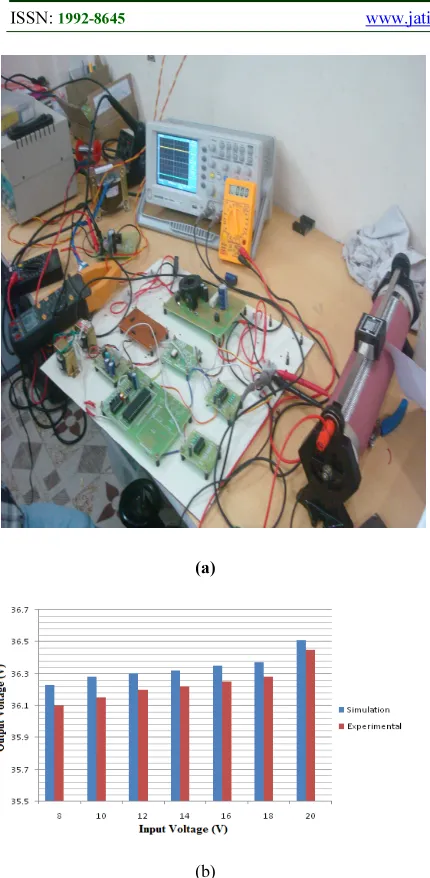
The main purpose of this section is to discuss about the experimental results of the POESLLC with designed ROLQR plus PDIC. The validation of the system performance is done for five different conditions through start-up transient, line variation, load variation, steady state region and also circuit components variations. The laboratory prototype and MATLAB/Simulink simulation models are performed on the POESLLC circuits with specifications listed in Table 1. The experimental block diagram model of the POESLLC with the implemented ROLQR plus PDIC is shown in Fig.3. The details of the power circuits are as follows:
Q IRFP 260 (MOSFET);
D1 - D2 FR306 (Diodes);
C1 – CO 30 µF/200V (Electrolytic and plain polyester type)
[image:9.595.298.504.289.567.2]L1 100µH/5A (Ferrite Core)
Figure 8. Experimental Block Diagram Model Of The POESLLC Using A ROLQR Plus PDIC In Digital
Platform.
The parameters of the controller are K1=1,
K2=0.09, Kp = 0.01, Ti s =0.0011s and 0.00621s
as calculated in the previous section. The controller parameter of ROLQR plus PDIC is implemented in digital dsPIC30F4011 controller platform (refer the Fig. 3). In closed loop operation, measured values of the input voltage, the inductor current and output voltage are scale down to smaller than ± 10V with help of signal conditioning circuit and isolation circuit. The ADC signals are processed by designed controller
algorithm to compute the new duty cycle of power switch Q. The PWM pulse is derived from dsPIC30F4011 and it is applied to trigger MOSFET of the POESLLC using opto-coupler and driver IR2110. The main aim of the opto-coupler 6N137 is used for isolation between the power circuit and control unit. The function of the driver circuit IR 2110 is utilized to magnify the pulses of the MOSFETs. The main features of the digital dsPIC30F4011 controller are listed in
Table.5 Main Features Of Digital Dspic30f4011 Controller
Features Details
Architecture instructions, 16-bit wide data path 84 base instructions, 24-bit wide
Operating frequency
0 to 40 MHz external clock input, 4 MHz-10 MHz oscillator input with
PLL active (4x, 8x, 16x) Power supply
voltage 2.5V to 5.5V Input/output 40 pins
Memory
Enhanced Flash program memory: 10,000 erase/write cycle (min.) for industrial temperature range, 100K (typical).Data EEPROM memory: 100,000 erase/write cycle (min.) for industrial temperature range, 1M
(typical).
A/D converter
10-bit Analog-to-Digital Converter (A/D) with 4 S/H Inputs: 500 Ksps conversion rate, - 9 input channels, conversion available during Sleep
and Idle
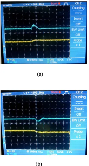
5.1 Line Variation
[image:9.595.97.275.387.561.2]
(b)
Figure 9. Experimental responses of output voltage
and input voltage of POESLLC with R = 50Ω using
ROLQR plus PDIC, (a) for input step change from 12V to 15V at time of 0.05s and
(b) For input step change from 12V to 09V at time of 0.05s [Ch1:10V/Div-input voltage and Ch2:10V/Div- output voltage].
5.2 Load Variation
(a)
(b)
Figure 10. Experimental response of output voltage of
POESLLC with Vin = 12 V using ROLQR plus PDIC,
(a) when load value takes a step changes from 50 Ω to
40Ω and (b) when load value takes a step changes
from 50Ω to 70Ω at time 0.05s [Ch1:10V/Div-input
voltage and Ch2:200 mA/Div- output current].
5.3 Circuit Components Variations
(a)
[image:10.595.87.500.90.631.2]
(b)
Figure 11. Experimental output voltage of POESLLC at circuit components variations using the designed controller, (a) when inductor variation from 100µH to 150µH, (b) when capcitor variation from 30µF to 100µF) [Ch1:10V/Div-output voltage].
[image:10.595.98.255.386.678.2]
(a)
[image:11.595.79.515.94.551.2]
(b)
Figure 12 . Photograph Model And Perofomance Of POESLLC Using Designed Controller Is Expressed
In Graphical Representation, (A)Laboratory Prototype Set Up Model,(B) Graphical Imulated
And Experimental Output Voltage Resultsat Diferent Input Voltage.
Fig. 12(a) indicates the photograph of laboratory prototype set-up model of POESLLC using ROLQR plus PDIC.Fig.12 (b) show the graphical results of experimental and simulated output voltage of POESLLC using the controller for varying input voltage range from 8V to 20V. From this figure, it is clearly showed that output voltage deviation is 0.18 V for complete input voltage changes. In addition, the same model can be work in large power rating with require of high level design. In summary, from the Figs. 5 to 9, it
is clearly indicated that the experimental results of the POESLLC using a designed ROLQR plus PDIC match the simulated results. Finally, a designed ROLQR plus PDIC performed
well in all the working conditions of the converter. The above figure shows signifies the graphical form of simulation and experimental results of % efficiency of the POESLLC using a ROLQR plus PDIC at rated load condition. From this figure, it is clearly found that the % efficiency of the POESLLC using a ROLQR plus PDIC has maintained 91.27%.
6. CONCLUSIONS
The design of ROLQR plus PDIC using sliding surface co-efficient for POESLLC operated in CCM has been successfully established in MATLAB/Simulink. The designed controller co-efficient have been implemented in digital platform (dsPIC30F4011 controller). The main merits of designed controller over a conventional controller are robust to huge disturbances on input supply voltage and load resistance, trouble-free implementation and circuit parameter deviations without changing the controller coefficients. The results are presented to demonstrate the success of the designed ROLQR plus PDIC for the POESLLC worked in CCM resulted in quick dynamic response, good regulated output voltage, and excellent output voltage in the circuit component variations, wonderful steady state and transient responses. It is, as a result, appropriate for any stable power supply real-world commercial applications, and it is essentially intended for power source in LED TV, mobile phones, and computer hardware.
REFERENCES
[1] Abutbuli, O., Gherlitz, A., Berkovich, Y., Ioinovici, and A.: Step-up switching-mode converter with high voltage gain using a switched-capacitor circuit. IEEE Transactions on Circuits Systems. I. 50, 1098−1102 (2003)
[2] Comines, P., Munro, N.: PID controllers: recent tuning methods and design to specification. IEEE Proc. Control Theory Application. 149, 46-53 (2002)
[image:11.595.83.298.106.545.2][4] F.H.F. Leung, P.K.S. Tam, C.K. Li: The
control of switching DC–DC converters – A general LQR problem. IEEE Transactions on Industrial Electronics. 38, 65–71(1991) [5] Jiao, Y., Luo, F.-L., Zhu, M.: Generalized
modeling and sliding mode control for n-cell cascade super-lift DC-DC converters. IET Power Electron. 4, 532-540 (2011)
[6] Katshika Ogata: Modern Control Engineering. Published by Prentice – Hall of India Private Limited. New Delhi, Third Edition (1997)
[7] K. Ramash Kumar, S. Jeevananthan: A Sliding Mode Control for Positive Output Elementary Luo Converter. Journal of Electrical Engineering, 10, 115-127 (2010) [8] K. Ramash Kumar, S. Jeevananthan: Design
and implementation of reduced-order sliding mode controller plus proportional double integral controller for negative output elementary super-lift Luo-converter. IET Power Electron. 6, 974–989 (2013)
[9] Luo,F., Ye, H.: Positive output super lift converters. IEEE Transaction on Power Electronic. 18, 105-113 (2003)
[10]Luo, F.-L., Hong Ye: Advanced DC/DC Converters. CRC Press and Taylor &Francis Group. London. New York. (2006)
[11]Lu, D.D.C., Cheng, D.K.W., Lee, Y.S: A single-switch continuous conduction-mode boost converter with reduced reverse-recovery and switching losses. IEEE Trans. Ind. Electron. 50, 767–776 (2003)
[12]Mattavelli, P., Rossetto, L., Spiazzi. G.: Small signal analysis of DC-DC converter with sliding mode control. IEEE Transaction on Power Electronics. 12, 96-102 (1997) [13]Middlebrook, R., Cuk, S.: A General Unified
Approach to Modeling Switching-Converter Power Stages. International Journal of Electronics. 42, 521-550 (1977)
[14]Martinez-Salamero, L., Cid-Pastor, A., Giral, R., Calvente, J., Utkin. V: Why is Sliding Mode Control Methodology Needed for Power Converters?. Proceedings of 14th International Power Electronics and Motion Control Conference (short form of the conference). S9-25-31 (2010)
[15]Mahdavi, J., Emadi, A., Toliyat, H.-A.: Application of state space averaging method to sliding mode control for PWM DC/DC converters. IEEE Industry Application Society Annual Meeting, New Orieans, Louisianan, 820-827 (1997).
[16]Sira-Ramirez, H: On the generalized PI sliding mode control of DC-to-DC power converters: a tutorial. Int. J. Control. 76, 1010-1033 (2003)
[17]Sudip K. Mazumder, Muhammad Tahir, and Kaustuva Acharya: Master–Slave Current-Sharing Control of a Parallel DC–DC Converter System over an RF Communication Interface. IEEE Transaction on Industrial Electronics, 55, 59-66 (2008) [18]Tseng, C., Liang, T.J.: Novel high-efficiency
step-up converter. IEE Proc. Electr. Power Appl.151, 182−190 (2004)
[19]Tan, S.-C., Lai, Y.-M., Chi K Tse, Luis Martneiz Slamero, Chi-Kin Wu: A Fast response sliding mode controller for boost type converter with a wide range of operating condition. IEEE Transactions on Industrial Electronics, 54, 3276- 3286 (2007)
[20]Umamaheswari.M.G,Uma.G.Vijayalakshmi. K..M., Design and implementation of reduced-order sliding mode controller for higher-order power factor correction converters. IET Power Electron., 4, 984–992 (2011)
[21]Umamaheswari.M.G,Uma.G, Vijayalakshmi, K.M.: ‘Analysis and design of reduced-order linear quadratic regulator control for three phase power factor correction using Cuk converters. Electric Power System Research. 96, 1–8 (2013)
[22]Viera Biolkova, Zdenek Kolka, Dalibor Biolek: State-Space Averaging (SSA) Revisited: On the Accuracy of SSA-Based Line-To-Output Frequency Responses of Switched DC-DC Converters. WSEAS Transactions on Circuits and Systems. 9, 81- 90 (2010)
[23]Veerachary, M.: General rules for signal flow graph modeling and analysis of dc–dc converters. IEEE Trans. Aerosp. Electron. Syst. 40, 259–271(2004)
[24]Y. He, Y., Luo, F.-L.: Study of sliding mode control for dc–dc converters. International Conference on Power System Technology (POWERCON 200), Singapore, 1969-1974 (2004)