Available Online at www.ijpret.com 54
INTERNATIONAL JOURNAL OF PURE AND
APPLIED RESEARCH IN ENGINEERING AND
TECHNOLOGY
A PATH FOR HORIZING YOUR INNOVATIVE WORK
ANTENNA-ON-CHIP FOR WIRELESS APPLICATIONS: MODELLING AND
SIMULATION ANALYSIS
PATIL RR1, VANI RM2, HUNAGUND PV3 1. Research Scholar, Dept. of Applied Electronics, Gulbarga University-585106 2. Professor, University Science Instrumentation Centre, Gulbarga University-585106 3. Professor, Dept. of Applied Electronics, Gulbarga University-585106
Accepted Date: 24/10/2014; Published Date: 01/11/2014
\
Abstract: This paper presents modeling and simulation characterization of radiating copper nanofilm based microstrip patch antenna for on-chip wireless systems around 20 GHz (K-Band). The proposed antenna uses high resistivity silicon wafer as substrate on which, the copper nanofilm forms radiating element. The antenna structure uses a scheme known as coplanar waveguide fed proximity coupled patch in order to avoid soldering high resistivity nanofilm and very low resistivity bulk feed. The nanofilm antenna design is modeled and simulated in IE3D software shows excellent performance in terms of impedance bandwidth, 57.66% higher over bulk patch antenna. The nanofilm antenna can be fabricated along with IC technology fabrication on the same silicon wafer substrate.
Keywords: Nanofilm, coplanar proximity coupled patch antenna, antenna-on-chip, inter and intra-chip communication
Corresponding Author: MR. RAJENDRA R. PATIL
Access Online On:
www.ijpret.com
How to Cite This Article:
Available Online at www.ijpret.com 55 INTRODUCTION
On-chip antennas are tiny surface mount devices designed to provide inter and intra-chip wireless communication or for short range of air transmission. The typical on-chip antenna integrated with analog and digital circuitry on the same wafer finds applications in wireless LAN, GPS receiver, Bluetooth and cellular transceivers [1]. Earlier, antennas have to be interfaced with chip circuit using bond wires (off-chip). An on-chip antenna fabrication avoids the requirement of bond wires or off the chip components. Thus the on-chip antenna fabrication provides a robust solution in smaller form factors [2]. Furthermore monolithic fabrication of the antenna with RF electronics reduces power losses and parasitic effect compared to integration of discrete components. To achieve antenna integration within a single chip, different solutions have been suggested [3-4-5]. Silicon substrate allows the antenna coupling on a chip with RF electronics. Antenna integration with silicon has been demonstrated in [6-7]. However, most of them are either bulky or having narrow bandwidth. In this work copper nanofilm is modeled instead of bulk copper as antenna radiating element. There are two advantages by employing copper nanofilm, first, the density of antenna decreases, and second, improvement in impedance bandwidth due to high surface resistivity of nanofilm. The increase in high surface resistivity increases bandwidth. To our knowledge, for the first time we are modeling an on-chip nanofilm antenna using coplanar waveguide (CPW) proximity coupled antenna through simulation to decrease the density of antenna, enhancing the bandwidth and increasing return loss.
ON-CHIP ANTENNA DESIGN
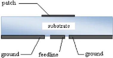
Available Online at www.ijpret.com 56 on both sides that is approximately 2 μm thick, instead of gold. Figure 2 illustrates side view of the CPW proximity coupled patch antenna. Third, for 30 nm thickness which is less than electron mean free path of copper, the surface resistivity is calculated using Fuchs-Sondheirmer equations [10]. The resonant frequency is controlled by varying the gap between feedline and ground, stub from centre of the substrate and patch dimensions.
Figure 1 Geometry of CPW proximity coupled patch antenna.
Figure 2 Geometry of CPW proximity coupled patch antenna: side view
RADIATING PATCH THICKNESS MODELING
Available Online at www.ijpret.com 57 (a) (b)
Figure 3 Radiating patch (a) finite thickness model (b) infinite thin strip model
ANTENNA MODELING
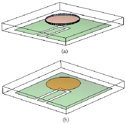
The complete CPW proximity coupled patch antenna is modeled for both bulk thickness patch and nanofilm thin thicknesses are illustrated in fig. 4. The simulation model of antenna has substrate and ground plane of 8 by 8 mm, and the high resistivity silicon wafer is 0.5 mm thick with a permittivity of 11.9, a material loss tangent of 0.015, and conductivity of 0.025 S/m. The metallic dimensions of antenna are: a 50Ω CPW feedline length and width of 4.65 by 1 mm, gap between coplanar ground and feedline is 0.38 mm, circular patch radius of 1.15 mm. The CPW proximity coupled antenna uses circular disk as radiating patch. The main advantage of circular patch over rectangular patch is that circular patch occupies less physical area. Thus in applications such as arrays, circular geometries are preferred.
Available Online at www.ijpret.com 58 The 2 μm bulk copper electrical specifications are: conductivity (σ) of 5.8*107 S/m, permeability (μr) of 1, permittivity (εr) of 1. If the metal film thickness is larger than electron mean-free-path p, the resistivity ρ is expected to be nearly the same as that of a bulk metal patch. When the metal film thickness is less than the order of the electron mean-freepath, then the role of electron scattering becomes significant. Very thin metallic films have a much higher resistivity than a bulk metal because of electron scattering from the metal film surface. For nanofilm of 30 nm, the conductivity f σ is computed using the following Eq. 1 [10],
f
3tσ p
σ = ln +0.4228 S/m
4p t
For t << p (1)
Where σ is bulk copper patch conductivity, t is patch thickness and p is electron path in meters. Equation 1 holds good only if film thickness t is less than electron mean-free-path p. The surface resistance Rs of nanofilm is independent of the dimensions of the square and equals, is given by:
s f
1
R = Ω/square
t.σ
(2)
According to the Fuch-Sondheimer theory, the surface resistance of a metallic film decreases as the thickness of the film increases. For our work we have selected thickness t of copper patch as 30 nm for antenna application which is less than electron mean-free-path p of copper (42 nm). The conductivity and surface resistivity of 30 nm copper patch is computed for thickness less than electron mean-free-path using Eq. 1 and 2. The computed values are listed as
Conductivity of nanofilm: σf= 2.43*107 S/m (3)
Surface Resistance: Rs = 1.371 Ω/sq (4)
From the computation, it is observed that at patch thickness less than electron mean free path, there is decrease in the conductivity and increase in the surface resistance when compared to bulk thickness patch. For nanofilm modeling, numerical values in Eq. 3 and 4 are used in IE3D simulation.
ANTENNA SIMULATION
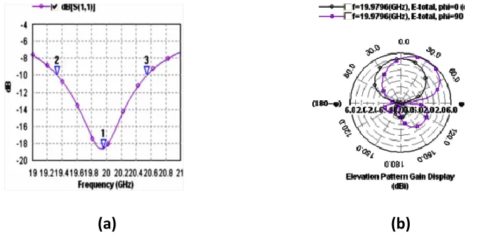
Available Online at www.ijpret.com 59 general 3D and planar structures like patch antennas. It solves Maxwell’s equation and its solutions include discontinuity effects, wave effects, coupling effects, and radiation effects. The modeled antennas are simulated with finite ground from 19 GHz to 21 GHz frequency ranges. The operating frequency (fr), return loss (RL), bandwidth (BW), and gain were obtained from
simulated reflection coefficient S11 graph and 2D radiation pattern as shown in fig. 5 and 6 respectively.
(a) (b)
Figure 5 Bulk Patch Antenna (a): Return loss vs. frequency, (b): 2D radiation pattern
(a) (b)
Figure 6 Nanofilm antenna (a): Return loss vs. frequency, (b): 2D radiation pattern
Available Online at www.ijpret.com 60 max min
r
f -f
BW (%) = 100 f
(5)
Where fmax and fmin are maximum and minimum frequency, at -10 dB points, and fr is resonant frequency.
TABLE 1 SIMULATED RESULT FOR BULK PATCH AND NANOFILM ANTENNA
Antenna
Type
Antenna parameters after Simulation
fr (GHz) RL (–dB) BW (GHz) Gain (dBi) BW (%)
Bulk patch 19.97 14.78 0.509 5.63 2.54
Nanofilm 19.93 18.62 1.210 1.42 6.00
RESULTS AND DISCUSSION
Available Online at www.ijpret.com 61 useful in applications where short range chip-to-chip, intra-chip communication with higher data rates is required.
CONCLUSION
This paper has presented the effect of nanofilm radiating patch on antenna performance for wireless Microsystems applications. Copper nanofilm of 30 nm thickness less than electron mean-free-path of 42 nm is modeled over 0.5 mm high resistivity silicon wafer substrate for CPW proximity fed microstrip patch antenna. The CPW proximity fed antenna provides contactless electromagnetic coupling between nano thickness patch and bulk feedline, without having to be reliable contact. The antenna is simulated using IE3D method of moments based full wave simulator for radiation characterization. The simulation shows encouraging results in terms of enhanced wide bandwidth and higher return loss around 20 GHz. The large bandwidth is highly suitable for compact, high data rate System-on-Chip (SoC) applications and in intra-chip communication such as wireless global clock distribution system. With recent developments in nonmaterial’s and nanotechnology systems/tools like PVD, CVD, sputtering etc, it is possible to fabricate nanofilm patch antenna on low loss high resistivity thin silicon wafer.
ACKNOWLEDGEMENTS
The authors acknowledge thanks to UGC, New Delhi for sanctioning the Mentor Graphics IE3D simulation software sanctioned to Gulbarga University under major research project which is most useful and reliable for designing microstrip patch antennas. Author R.R.P would like to convey sincere thanks to President Poojya Dr. Sharanabaswappa Appa, Principal Dr. V.D. Mytri, and Dean (Admin) Dr. Anilkumar G. Bidve of Appa Institute of Engineering and Technology, Gulbarga for constant support and encouragement to carry out the research work.
REFERENCES
1. A. A. Abidi, “RF CMOS comes of age," Solid-State Circuits, IEEE Journal of, vol. 39, pp. 549-561, 2004.
2. Gabriel M. Rebeiz, RF MEMS: Theory, design, and technology, John Wiley & Sons, New Jersey, 2003.
Available Online at www.ijpret.com 62 4. Zhang, Y.P., “Integration of Microstrip Patch Antenna on Ceramic Ball Grid Array Package”, Electron. Lett., Vol. 38 No 5, pp. 207-208, February 2002.
5. Garg, R., Bhartia, P., Bahl, I., Ittipiboon, A., Microstrip Antenna Design Handbook, Artech House, 2001.
6. H. R. Chuang, L.K. Yeh, P. C. Kuo, K. H. Tsai, H. L. Yue, “ A 60-GHz Millimeter-Wave CMOS Integrated On-Chip Antenna and Bandpass Filter”, IEEE Transactions on Electron Devices, Vol. 58, no. 7, pp. 1837-1845, 2011.
7. Y. P. Zhang, L. H. Guo, M. Sun, “High Transmission Gain Inverted-F Antenna on Low Resistivity Silicon for Wireless Interconnect”, IEEE Electron Device, vol. 27, no. 5, pp. 374-376, 2006.
8. R. N. Simons, R. Q. Lee, G. R. Lindamood, “Electromagnetic Coupling between Coplanar waveguide and Microstrip antennas”, Microwave and Optical Technology Letters, Vol. 5, issue 2, pp. 60-62, February 1992.
9. Theodore K. Anthony, “Wafer Level Antenna Design at 20 GHz”, U.S. Army Research Laboratory, Sensors and Electron Devices Directorate, ARL, pp. 1-20, April 2008.
10.Samuel Y. Liao, Microwave Devices and Circuits, Pearson Education, Inc. New Delhi, 2003.