Copyright © 2014 IJECCE, All right reserved
A Multi Band Low Noise Amplifier as a Front End for
Multi-standard Receiver Wireless Network
Shinde Jitendrakumar N.
Associate ProfessorISB&M SOT College of Engineering, Pune Email: [email protected]
Dr. S. K. Bodhe
Director BoSh Technology, Pune Email: [email protected]Abstract – The multi-band low noise amplifier can operates on different frequency band. In lower band will works on frequency band 700MHz to 1200 MHz and upper frequency band operates on 1700MHz to 2300MHz.In this external gate source capacitor is used for the input impedance matching. The noise figure is 4.05 and 3.59 for lower and upper band respectively.
Keywords – LNA, Cex1, GATE SOURCE CAPACITANCE, IDCS.
I. INTRODUCTION
With the progress of wireless communications requirements for transceivers that can support multi-bands and multi-standards. The key bottleneck for multiple-standard communications is the implementation of the low- noise amplifier. This can operate at different frequency bands, which plays an important role in the noise performance or sensitivity of the band, multi-standard receiver. The challenges include an input matching, frequency response of power gain, noise figure, and good linearity within the desired bands. A basic approach implements multiple separated narrowband amplifiers, each designed for a different frequency band. Apparently this method undergoes from high power dissipation, a large chip area.
There are three ways of implementing a multi-band LNA. The first way is to use a separate LNA for each standard, resulting in larger die area, higher cost and power. The second way is to use a wideband LNA. It offers the smaller area and power, the sensitivity suffers with large out-of-band unwanted blocker due to the non-linearity of the transistor. The third method is use the concurrent dual-band LNA that offers better trade-off between area, power and sensitivity.
The design of multi-band design of these wide band low noise amplifiers implemented for lower and upper bands. The lower frequency band is from 700MHz to 1200MHz and upper frequency band from 1700MHz to 2300MHz respectively. The main goal of this investigation is to design and implementation of a single reconfigurable multi-band multi-standard low noise amplifier. This low noise amplifier will be designed in such a way that the reconfigurability is achieved by changing of hardware configuration to support these frequency bands. This low noise amplifier is use for the multi-band multi-standard mobile receiver. The multi-band low noise receiver is used an inductively degenerated common source topology. The IDCS topology is cover lower band as well as upper band frequencies. This multi-band low noise amplifier is use the
external gate source capacitor. This capacitor is used for the input impedance matching.[1]
The paper is organized as follows: Section I gives introduction information of multi-band low noise amplifier. In the section II we present the design of multi-band low noise amplifier, mathematical calculations and circuit diagram. In section III circuit diagram and simulated results such as scattering parameters, linearity and noise figure calculation are presented. For the purpose of design and implementation we use Agilent’s ADS simulator. In Section IV we present the Layout implementation, Simulation and measurement results. In section V we present conclusion and future scope.
II. PROCEDURE
A.
Design of multi-band LNA
Fig.1 indicates the schematic circuit diagram of multi-band widemulti-band inductively degenerated common source LNA targeted to cover the carrier frequency range from 700 MHz to 1200 MHz for lower band and 1700 MHz a to 2300 MHz for upper band. Multi-band low noise amplifier is used lower values of inductor because it will operate in lower as well as upper band. The external gate source capacitance Cex1 and Cex2 are the external capacitor
required for both the band modes respectively. The external capacitor is used for the input impedance matching. CD1and CCD2 are used as load capacitance for
lower and upper band respectively. LG,LS, LD, Ll and Rl is
the input load inductor and load resistor. [2] [5]
Fig.1. A Schematic Circuit Diagram of Multi-Band Low Noise Amplifier
B.
Design parameter
Copyright © 2014 IJECCE, All right reserved transistor electronic switch SW0 whether it is in ON of
OFF mode, the LNA will operate either at upper band frequency or lower band frequency. [3]
The following equations are derived for the impedance matching at the input of multi-band low noise amplifier.
i) For upper band mode:
The first transistor SW0 is off condition. Cex = Cex1=Cgs ex, upper band
𝑍𝑖𝑛 ,𝑢𝑝𝑝𝑒𝑟 ,𝑏𝑎𝑛𝑑 ≈ 𝑠 𝐿𝐺+ 𝐿𝑆 +
𝑔𝑚1𝐿𝑠
𝐶𝑔𝑔1+ 𝐶𝑔𝑠,𝑢𝑝𝑝𝑒𝑟 𝑏𝑎𝑛𝑑
+ 1
𝑠 𝐶𝑔𝑔1+ 𝐶𝑔𝑠,𝑢𝑝𝑝𝑒𝑟 𝑏𝑎𝑛𝑑
𝑅𝑠=
𝑔𝑚1𝐿𝑠
𝐶𝑔𝑔1+ 𝐶𝑔𝑠,𝑢𝑝𝑝𝑒𝑟 𝑏𝑎𝑛𝑑
= 50𝛺
ii) For lower band mode:
Cex = Cex1 + Cex2= Cgs ex, lower band
𝑍𝑖𝑛 ,𝑙𝑜𝑤𝑒𝑟 𝑏𝑎𝑛𝑑 ≈ 𝑠 𝐿𝐺+ 𝐿𝑆 +
𝑔𝑚1𝐿𝑠
𝐶𝑔𝑔1+ 𝐶𝑔𝑠,𝑙𝑜𝑤𝑒𝑟 𝑏𝑎𝑛𝑑
+ 1
𝑠(𝐶𝑔𝑔1+ 𝐶𝑔𝑠 ,𝑙𝑜𝑤𝑒𝑟 𝑏𝑎𝑛𝑑)
𝑅𝑠=
𝑔𝑚1𝐿𝑠
𝐶𝑔𝑔1+ 𝐶𝑔𝑠,𝑙𝑜𝑤𝑒𝑟 𝑏𝑎𝑛𝑑
= 50𝞨
For the output impedance matching, SW1 and SW2 participates important roles in to decide the load at the output. The on and off positions of these switches will set the output impedance matching of the LNA either to operate at upper band or lower band mode.
For the upper band mode SW1 has to be in ON condition and SW2 in off condition. In this situation R1 and L1 is in
series. So to calculate the output impedance matching of low noise amplifier following equations is revised. For upper band
𝑌𝐿 𝑢𝑝𝑝𝑒𝑟 𝑏𝑎𝑛𝑑 = 𝑠𝐶𝐷1+
1 𝑟 + 𝑠𝐿𝐷
+ 1
𝑅𝑠𝑤1𝑅1+ 𝑠𝐿1
𝑍𝐿 𝑢𝑝𝑝𝑒𝑟 𝑏𝑎𝑛𝑑 =
1 𝑌𝐿 𝑢𝑝𝑝𝑒𝑟 𝑏𝑎𝑛𝑑
= 1
𝑠𝐶𝐷1
𝑟 + 𝑠𝐿𝐷 𝑅𝑢𝑝𝑝𝑒𝑟 𝑏𝑎𝑛𝑑 + 𝑠𝐿1
=𝑅𝑢𝑝𝑝𝑒𝑟 𝑏𝑎𝑛𝑑𝑟 + 𝑠 𝑅𝑢𝑝𝑝𝑒𝑟 𝑏𝑎𝑛𝑑𝐿𝐷+ 𝑟𝐿1 + 𝐿1𝐿𝐷𝑠
2
1 + 𝑠𝐶𝐷1 𝑅𝑢𝑝𝑝𝑒𝑟 𝑏𝑎𝑛𝑑 + 𝑟 + 𝑠2𝐶𝐷1 𝐿1+ 𝐿𝐷
At lower band mode SW1 has to be in OFF condition and SW2 in ON condition. Only R1 and L1 are representing
the resistance. With the total capacitance (𝐶𝐷1+
𝐶𝐷2) 𝑎𝑛𝑑 𝐿𝐷 will set the output impedance matching for lower band mode.
So, for lower band
𝑌𝐿 𝑙𝑜𝑤𝑒𝑟 𝑏𝑎𝑛𝑑 = 𝑠(𝐶𝐷1+ 𝐶𝐷2) +
1 𝑟 + 𝑠𝐿𝐷
+ 1
𝑅1+ 𝑠𝐿1
∴ 𝑍𝐿 𝑙𝑜𝑤𝑒𝑟 𝑏𝑎𝑛𝑑 =
1
𝑌𝐿 𝑙𝑜𝑤𝑒𝑟 𝑏𝑎𝑛𝑑 = 1
𝑠𝐶𝐷 ,𝑙𝑜𝑤𝑒𝑟 𝑏𝑎𝑛𝑑
𝑟 + 𝑠𝐿𝐷 𝑅𝑙𝑜𝑤𝑒𝑟 𝑏𝑎𝑛𝑑 + 𝑠𝐿1
= 𝑅𝑙𝑜𝑤𝑒𝑟 𝑏𝑎𝑛𝑑𝑟 + 𝑠 𝑅𝑙𝑜𝑤𝑒𝑟 𝑏𝑎𝑛𝑑𝐿𝐷+ 𝑟𝐿1 + 𝐿1𝐿𝐷𝑠
2
1 + 𝑠𝐶𝐷 𝑅𝑙𝑜𝑤𝑒𝑟 𝑏𝑎𝑛𝑑 + 𝑟 + 𝑠2𝐶𝐷 𝑙𝑜𝑤𝑒𝑟 𝑏𝑎𝑛𝑑 𝐿1+ 𝐿𝐷
Where
R upper band =R sw1*R1 and R lower band =R1
CD, lower band=CD1+CD2
iii) Calculation of gain of the multi-band low noise
amplifier
Gain of upper band
𝑆21= 2 ×
𝑣𝑜𝑢𝑡
𝑣𝑖𝑛
𝑆21= 𝐺𝑀21(𝑠) × 𝑍𝐿 𝑢𝑝𝑝𝑒𝑟 𝑏𝑎𝑛𝑑(𝑠)
Gain of lower band
𝑆21= 2 ×
𝑣𝑜𝑢𝑡
𝑣𝑖𝑛
𝑆21= 𝐺𝑀21(𝑠) × 𝑍𝐿 𝑙𝑜𝑤𝑒𝑟 𝑏𝑎𝑛𝑑(𝑠)
III. CALCULATION
Now, find out the cutoff frequency
𝜔 = 2П𝑓 = 2П× 2𝐺𝐻𝑧
= 12.56 G rad/sec
The value of Ls is arbitrary value and it should be below
0.55 nH. Unnecessary source inductance can lead to LNA oscillations because of gain peaks at higher range frequencies. For this design we assumed the value of 0.55 nH.
So we assume Ls=0.55 nH.
𝜔𝑇 =
𝑔𝑚
(𝐶𝑔𝑠+ 𝐶𝑑)
=𝑅𝑠 𝐿𝑠
= 50
0.1𝑛𝐻= 500𝐺 𝑟𝑎𝑑/𝑠𝑒𝑐
The value of Q is given by
𝑄 = 1 +1𝑝 Where p = 𝛿𝛼 2
5𝛾
The parameters for p are dependent on the CMOS technology but typically α is assumed to be 0.8 -1.0 (normally 0.9) δ is set to 2 - 3 times the value of (take to be 4) γ is set between 2 - 3 (normally 2)
𝑄 = 1 +1
𝑝
= 2.67
Evaluation of LG
𝑄 =𝜔0(𝐿𝐺+ 𝐿𝑆) 2𝑅𝑠
𝐿𝐺=
2𝑄𝑅𝑠
𝜔0 -𝐿𝑠
The source degenerated inductance Ls can be calculated
by the following equation:
𝑅𝑠= 𝑔𝑚𝐿𝑠
Copyright © 2014 IJECCE, All right reserved Unnecessary source inductance can lead to LNA
oscillations because of gain peaks at higher range frequencies. For this design we assumed the values of 0.55 nH.
𝐿𝐺=
2 × 2.67 × 50
12.56 × 10⁹ − 0.55 × 10
−9
= 20.70 nH
Calculation of LD
𝐿𝐷 =
1 𝜔2𝐶
𝐿
Assume 𝐶𝐿=100fF
𝐿𝐷 =15.60 nH
To find gate source capacitance Cgs
𝐶𝑔𝑠 𝑢𝑝𝑝𝑒𝑟 =
1 𝜔02(𝐿
𝐺+ 𝐿𝑆)
𝐶𝑔𝑠 𝑢𝑝𝑝𝑒𝑟 =
1
12.56 × 10⁹ 2(21.15 𝑛𝐻 + 0.1𝑛𝐻)
𝐶𝑔𝑠 𝑢𝑝𝑝𝑒𝑟 = 0.298 × 10⁻¹²𝑓
𝐶𝑔𝑠 𝑙𝑜𝑤𝑒𝑟 =
1 𝜔02(𝐿𝐺+ 𝐿𝑆)
𝐶𝑔𝑠 𝑙𝑜𝑤𝑒𝑟 =
1
5.93 × 10⁹ 2(43𝑛𝐻 + 0.1𝑛𝐻)
𝐶𝑔𝑠 𝑙𝑜𝑤𝑒𝑟 = 0.6666 × 10⁻¹⁵𝑓
Calculation of Cd
𝑅𝑠= 𝑔𝑚𝐿𝑠
(𝐶𝑔𝑠+𝐶𝑑) = 50 𝛺
But the transcondutance
𝑔𝑚 𝑢𝑝𝑝𝑒𝑟 = 𝜔𝑇∙ 𝐶𝑔𝑠
𝑔𝑚= 500 × 109× 0.298 × 10−12
= 0.149 𝑚𝐴/𝑉
𝑔𝑚 𝑙𝑜𝑤𝑒𝑟 = 𝜔𝑇∙ 𝐶𝑔𝑠
𝑔𝑚 𝑙𝑜𝑤𝑒𝑟 = 500 × 109× 0.666 × 10−15
= 333.333 𝑚𝐴/𝑉
The above equations show that 𝐶𝑔𝑠 of lower band is higher than 𝐶𝑔𝑠 of upper band. Therefore the ending current of low noise amplifier operating at lower band frequency has to be higher than the ending current of the low noise amplifier operating at upper band.
Re-arranging the equation
𝐶𝑔𝑠+ 𝐶𝑑 = 𝑔𝑚𝐿𝑠
𝑅𝑠 = 50 𝛺
0.298 × 10⁻¹²+ 𝐶
𝑑 =
0.00149 × 0.1 𝑛𝐻 50 ∴ 𝐶𝑑= 295.58 × 10⁻¹⁵𝑓
Calculation of dimension of M1
𝑊 =3
2 𝐶𝑔𝑠
𝐶𝑜𝑥𝐿𝑚𝑖𝑛
𝐿𝑚𝑖𝑛 = 0.6 × 10⁻⁶ 𝑎𝑛𝑑 𝑇𝑜𝑥 = 1.01 × 10⁻⁸
𝜀𝑜𝑥 = 𝜀𝑠𝜀0
εs= a dielectric constant for silicon material =3.9
ε0=a dielectric constant for the free space =8.85*10-12
So the calculated value of εox=3.9*8.85*10-12
𝐶𝑜𝑥 =
∈0𝑥
𝑇𝑜𝑥
= 3.14 × 10⁻³𝑝𝐹
So
𝐶𝑜𝑥 = 3.14 × 10⁻³𝑝𝑓
W = 237μm. Calculation of Qin
𝑄𝑖𝑛 =
1 2𝜔𝑜𝑅𝑠𝐶𝑔𝑠+ 𝐶𝑑
𝑄
𝑖𝑛 = 1
2×12.56×109×50×(0.298×10−12+295×10−15)
𝑄𝑖𝑛 = 2.45
Calculation of Gain:
The gain will be calculated by the following equation.
𝐺𝑚 = 𝑄𝑖𝑛𝑔𝑚 𝑢𝑝𝑝𝑒𝑟
= 3.65 × 10⁻³
Calculation of Veffecive
𝑉𝑒𝑓𝑓𝑒𝑐𝑡𝑖𝑣𝑒𝑣 =
𝑔𝑚𝐿𝑚𝑖𝑛
𝜇𝑛𝐶𝑜𝑥𝑊
n
is the device mobility=433cm/VVeffecive=0.717V
But Vt =0.67
So we need to apply total voltage
V=0.717+0.67=1.38V
Noise Figure
𝐹𝑢𝑝𝑝𝑒𝑟 = 1 +
𝛾 𝑔𝑚𝑅𝑠𝑄𝑖𝑛2
𝐹𝑢𝑝𝑝𝑒𝑟 = 1 +
2
0.00149 × 50 × (2.45)2
=5.47
𝐹𝑙𝑜𝑤𝑒𝑟 = 1 +
𝛾 𝑔𝑚𝑅𝑠𝑄𝑖𝑛2
𝐹𝑙𝑜𝑤𝑒𝑟 = 1 +
2
0.333 × 50 × (0.845)2
=1.17
IV. RESULTS
Copyright © 2014 IJECCE, All right reserved Fig.2. Simulated S11 versus frequency
Fig.3. Simulated S22 Versus Frequency
Fig.4. Simulated S12 Versus Frequency
Fig.5. Simulated S21 Versus Frequency
Fig.6. Simulated Noise Figure Versus Frequency
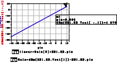
Fig.7. The IIP3 of Low Noise Amplifier
The figure for the above simulation results is shown in page no.8 the scattering parameter input reflection coefficient S11 measures the input return loss. The input
reflection coefficient of this low noise amplifier achieved is -32.361 dB. The scattering parameter output reflection coefficient S22 measures the output return loss. The output
reflection coefficient of this low noise amplifier achieved is -9.592 dB. The value of about -44.840 at peak frequency and it is a good reverse isolation. S21 forward /power gain
of low noise amplifier achieved 5.363 dB in the simulation. The simulated noise figure of low noise amplifier is 4.181 dBm. The simulated value of IIP3 is
4.279 dBm and it shown in simulated figure. The circuit has been achieved the best value of IIP3 with minimum
current consumption.[4]
II) Simulation Results for Upper Band
Fig.8. Simulated S11 Versus Frequency
Figure 9: Simulated S22 Versus Frequency
Copyright © 2014 IJECCE, All right reserved Fig.11. Simulated S21 Versus Frequency
Fig.12. Simulated Noise Figure Versus Frequency
Fig.13. The IIP3 of Low Noise Amplifier
The figure for the above simulation results is shown in page no.8. The input reflection coefficient of this low noise amplifier achieved is -11.929 dB. The input reflection coefficient should be below -10dB. The output reflection coefficient of this low noise amplifier achieved is -9.689 dB. Scattering parameters S12 i.e. reverse
isolation achieved in the simulation. The value of reverse isolation is about -34.696 dB at peak frequency. S21
forward /power gain of low noise amplifier achieved in the simulation. The simulation shows that the value of about 8.137 dB. The measured noise figure of low noise amplifier is 3.585 dB. This is between the optimum ranges of low noise amplifier. The simulated value of IIP3 is
11.384 dBm and it shown in simulated figure.
III) Comparison Chart of Upper and Lower Band
Fig.14. Comparison of S11 Versus Frequency For Lower
And Upper Band
Fig.15. Comparison of S22 Versus Frequency For Lower
And Upper Band
Fig.16. Comparison of S21 Versus Frequency For Lower
And Upper Band 700 750 800 850 900 950 1000 1050 1100 1150 1200
-35 -30 -25 -20 -15 -10 -5
FREQUENCY
S
1
1
(
d
B
)
S- Parameter (S11)
Simulated S11 Measured S11
1700 1800 1900 2000 2100 2200 2300 -13
-12 -11 -10 -9 -8 -7 -6 -5
FREQUENCY (MHz)
S
1
1
(
d
B
)
S- Parameter (S11)
Simulated S11 Measured S11
700 750 800 850 900 950 1000 1050 1100 1150 1200 -9.8
-9.6 -9.4 -9.2 -9 -8.8 -8.6
FREQUENCY
S
2
2
(
d
B
)
S- Parameter (S22)
Simulated S22 Measured S22
1700 1800 1900 2000 2100 2200 2300 -10.15
-10.1 -10.05 -10 -9.95 -9.9 -9.85 -9.8
FREQUENCY (MHz)
S
2
2
(
d
B
)
S- Parameter (S22)
Simulated S22 Measured S22
700 750 800 850 900 950 1000 1050 1100 1150 1200 1
2 3 4 5 6 7
FREQUENCY
S
2
1
(
d
B
)
S- Parameter (S21)
Simulated S21 Measured S21
1700 1800 1900 2000 2100 2200 2300 -36
-35.8 -35.6 -35.4 -35.2 -35 -34.8 -34.6
FREQUENCY (MHz)
S
1
2
(
d
B
)
S- Parameter (S12)
Copyright © 2014 IJECCE, All right reserved Fig.17. Comparison of S12 Versus Frequency For Lower
And Upper Band
Fig.18. Comparison of Noise Figure Versus Frequency For Lower And Upper Band
The results are divided into two types, simulated and measured as shown figures. The power gain S21 for the
simulated is about 6.5 dB at the center frequency while for measured gain is about 6.5 dB. The difference between these results is because of the parasitic values of the component. The input return loss for simulation is -32.361 dB and measured input return loss is -11 dB. The difference of simulated and measured is -34.30 dB.
For S22 the simulated resulted produced -9.5 dB at the
center frequency while without matching network the measured value is -9.7 dB obtained. The reverse isolation S12 obtained for simulated value is -45 dB and measured
values is -44.7 dB. The noise figure of the schematic circuit is around 4.05 dB at center frequency and measured value is 4.18 dB.
The power gain S21 for the simulated is about 8.00dB at
the center frequency while for measured gain is about 7.5 dB. The input return loss for simulation is -11.75 dB and measured input return loss is -12.00 dB. The difference of simulated and measured is -0.250 dB.
For S22 the simulated resulted produced -10.01 dB at the
center frequency while measured value is -10.15 dB obtained. The reverse isolation S12 obtained for simulated
value is -34.65 dB and measured values is -34.90 dB. The noise figure of the schematic circuit is around 3.59 dB at center frequency and measured value is 3.62 dB.
V. CONCLUSION
The multi-band low noise amplifier can operate at different frequency bands, which plays an important role in the noise performance or sensitivity of the multi-band, multi-standard receiver. The values of capacitors Cex1 and Cex2 have to be determined the matching conditions for upper band and lower band. For the output impedance matching, SW1 and SW2 decide the load at the output. The on and off positions of these switches will set the output impedance matching of the LNA either to operate at upper band or lower band mode.
REFERENCES
[1] Adiseno, Håkan Magnusson and Håkan Olsson “ A 1.8-V Wide-Band CMOS LNA for Multiband Multistandard Front-End Receiver”
[2] Mohd Tafir Mustaffa, Aladin Zayegh, Ronny, Tun Zainal Azni Zulkifli, “0.18 µm Fully Integrated 900 MHz CMOS LNA with Input and Output On-chip matching for Multi-standard Mobile Receiver”,2008 International conference on Microelectronics.
[3] Aly Ismail and Asad A. Abidi, “A 3–10-GHz Low-Noise Amplifier With Wideband LC-Ladder Matching Network”. IEEE
Journal Of Solid-State Circuits, Vol. 39, No. 12, December 2004.
[4] Pietro Andreani, Henrik Sjöland, “Noise Optimization of an Inductively Degenerated CMOS Low Noise Amplifier”. IEEE
Transactions On Circuits And Systems—Ii: Analog And Digital Signal Processing, Vol. 48, No. 9, September 2001.
[5] Adiseno, Håkan Magnusson and Håkan Olsson “ A 1.8-V Wide-Band CMOS LNA for Multiband Multistandard Front-End Receiver”
[6] Shinde Jitendrakumar Namdeo and Dr S. K. Bodhe “A 1GHz to 3GHz Design of Low Noise Amplifier for Multi-Standard Receiver” IJEST Vol.5, No.4 April 2013, Pp 665-676.
700 750 800 850 900 950 1000 1050 1100 1150 1200 -47
-46.5 -46 -45.5 -45 -44.5
FREQUENCY
S
1
2
(
d
B
)
S- Parameter (S12)
Simulated S12 Measured S12
1700 1800 1900 2000 2100 2200 2300 5.5
6 6.5 7 7.5 8 8.5 9
FREQUENCY (MHz)
S
2
1
(
d
B
)
S- Parameter (S21)
Simulated S21 Measured S21
700 750 800 850 900 950 1000 1050 1100 1150 1200 3.8
4 4.2 4.4 4.6 4.8 5
FREQUENCY
n
f
(2
)
Measured and simulated Noise Figure
Simulated NF Measured NF
1700 1800 1900 2000 2100 2200 2300 3.5
3.55 3.6 3.65 3.7 3.75 3.8 3.85 3.9
FREQUENCY (MHz)
n
f
(2
)
Copyright © 2014 IJECCE, All right reserved
AUTHOR’S PROFILE
Shinde Jitendrakumar N.
was born on June 25th 1975.He received his BE degree in the field of Electronics and Telecommunications Engineering in 1997 from Shivaji University, Kolhapur. He has completed ME in Electronics Engineering at GCOEP, affiliated to University of Pune in 2009. His research interests are in Wireless Communication He has 16 yrs of teaching experience. He has published Six Paper in International Journal and three papers in International and National Conferences.
Dr. S. K. Bodhe
born in Pune, India on Sept. 16th 1959. He received bachelor‟s degree in E & TC in 1983, M.E. in 1987 and Ph. D. in 1997 from Shivaji University, Kolhapur. He started his career as a R&D engineer turned teacher after 3 years. He became Assistant Professor in 1990 in Walchand College of Engineering in Sangli and Professor in 1999 in Pune Institute of Computer Technology. Currently he is working as a Principal, College of Engineering, Pandharpur, India. His area of interest is wireless networks.
Fig.19. Low Noise Amplifier For Lower Band