Abstract— As technology scaling has led to the integration of a large number of transistors into a chip, a large dedicated on-chip read-only memory (ROM) has not been a popular choice for designers. This is due to the fact that dedicated ROM designs require a sizeable amount of area. Large dedicated ROMs would not only increase chip cost/area but would also impair chip floorplan and result in interconnect delay. In this project we show that standard 6T and 8T static random access memory (SRAM) bit cells can embed ROM data without area overhead or performance degradation on the bit cells. Just by adding an extra wordline (WL) and connecting the WL to selected access transistor of the bit cell the bit cell can work both in the SRAM mode and in the ROM mode. In the ROM-embedded SRAM, during SRAM operations, ROM data is not available. During ROM mode operation SRAM data temporarily stored in buffer. With the ever-increasing complexity of present VLSI circuits, their testing is becoming more and more important. In this proposed project we will design a BIST circuit and we embedding R-SRAM circuit in BIST to test the circuit by using the test pattern generators which are produced by BIST.
Index Terms—Random access memory (RAM), read-only memory (ROM), ROM-embedded static RAM(SRAM), SRAM design, BIST.
I. INTRODUCTION
CMOS devices have been scaled down for about 40 years to achieve better performance, higher speed and low power consumption[1]. Due to their high speed and low power SRAM based memories are commonly used rather than DRAM. Although technology scaling has led to integration of large number of transistors,a large on-chip read only memory (ROM) has not been a wide choice for designers due to their consumption of large amount of area. Large on-chip ROMs also impairs chip floorplan resulting in interconnect delay.
Few examples of applications where “on-chip tables”
stored as read only memories can be effectively used are DSP, math
Manuscript received Nov, 2O15.
Kalakoti Krishna kumari,she is persuing MTECH of VLSI Department, JNTU university, sridevi women engineering College hyderabad, india .
Kalli siva nagi reddy, he is working as associate professer in ECE department.JNTU University/sridevi women college,hyderabad,india, function uses math function libraries stored in external nonvolatile memories. For such applications on chip ROM has significance as it improves performance. For evaluation
of math functions, math libraries are used. Such libraries are usually stored off-chip, leading to degradation in performance. Coefficients for fast Fourier transform library are stored in external nonvolatile memory[3] instead of on-chip ROMs. Coefficients for fast Fourier transform library are stored in external nonvolatile memory[3] instead of on-chip ROMs. Note that on-chip ROMs can significantly improve the performance of such applications. The interweaver for Turbo codes is designed by a dedicated logic to generate addresses on the fly, instead of dedicated on-chip ROMs[4] It should be noted that, even though nonvolatile data can be migrated into a faster external memory, such as dynamic random-access memory, the speed gap between a processor and an external memory grows with every technology generation, resulting in major road blocks to high-performance system design[5].
The most commonly used SRAM type is the 6T SRAM which is a standard in the industry because of its compact area, better tolerance to variability, and high performance[6]-[7] .The conventional 6T SRAM cell is made up of six MOSFET as shown in fig. 1, in which four transistors form the two cross coupled CMOS inverter (PL, PR, NL and NR). This is the place where a bit is stored either 1 or 0.The other two transistors (AXL, AXR) are called access transistor. It operates like pass transistors to control the access to SRAM cell by bit lines. The word line controls the functions of SRAM cell. If the WL is high the SRAM cell can be accessed. Otherwise SRAM cell is being isolated. In standby mode the word line WL is low, the access transistors will be off.
Fig.1: Conventional 6T SRAM design
The data stored in two crossed coupled inverter remain same.
There won’t be any change in its value as long as supply exits.
During write operation data is loaded to bit line first. Then
Test pattern generator through BIST for testing ROM-Embedded SRAM
k.krishna kumari, k.sivanagi reddy.
lines data will be stored in the two cross coupled CMOS inverter. In order to read, i.e. when data has been requested, the word line is being made high first. Before that bit lines should be precharged to VDD. As WL=1 the cell is being connected to bit lines. According to charge stored in two cross coupled inverters the bit lines will charge or discharge
This paper is organized as follows. SectionII, describes the proposed ROM Embedded SRAM cell operation of 6T R-SRAM cell, i.e SRAM mode operation and ROM mode operation based on word line connection. SectionIII, 8Transistor RSRAM cell design. In SectionIV, we test the R-SRAM circuit using BIST. Section V, describes the conclusion of the paper.
II. ROM Embedded 6T SRAM Cell
The proposed ROM Embedded SRAM (R-SRAM)[11]
design embeds ROM in SRAM. Storage cell acts as both SRAM and ROM hence no need to access external memory.
Fig.2: R-SRAM operation procedures in (a) normal SRAM mode and in (b) ROM mode.
The Existing 6T SRAM cell consumes more power and also volatile property i.e when the power is off total data will be erase. These disadvantages overcome by the proposed ROM Embedded SRAM cell
Storage cell works in two modes: SRAM and ROM
1. SRAM mode: Normal SRAM read write operation will be carried out and ROM data will not be available
2. ROM mode: When ROM data retrieval request is given SRAM data will be temporarily stored in buffer ,a two special write steps associated with connectivity of wordlines and access transistors is retrieves ROM data. After ROM data access SRAM data is transferred back to location.
The 6T ROM embedded SRAM[11] cell is implement with four NMOS transistors and two PMOS transistors and two word lines and bit lines. The schematic and layout of 6T R-SRAM bit cells storing “1001” (in ROM) are shown in Fig.
3. Unlike conventional 6T SRAMs, 6T R-SRAM bit cells have an extra WL. Depending on the ROM data to be embedded into the R-SRAM, the gate of an access transistor is connected to WL1 or WL2.The two neighbouring access transistors should be connected to the same WL, as shown in Fig. 3. If an R-SRAM bit cell stores “0”(“1”), the left access transistor (AXL) is connected to WL2(WL1). The right access transistor (AXR) of an R-SRAM[11] bit cell follows the connectivity of the AXL of the right-side neighbouring bit cell. Connectivity of the AXR of the end cell, which resides at the end of a row, is determined by the connectivity of the AXL of the end cell. During the normal SRAM mode, two WLs are always turned on and off at the same time so as to operate conventional 6T SRAM functions. In the ROM mode, to retrieve ROM data from R-SRAM, we perform the following two steps.
Step 1) Write “1”s to all the bit cells with WL1 and WL2 turned on (BL = 1, BLB = 0, WL1 = WL2 = 1).
Step 2) Write “0”s to all the bit cells with WL1 turned off and WL2 turned on (BL = 0, BLB = 1, WL1 =0, WL2=1).
Fig.3: Schematic of 6T R-SRAM bit-cells storing “1001.”
Fig.4: Layout of 6T R-SRAM bit-cells storing “1001.”
After step 1, the row stores “1111.” Following step 2,the row of Fig.3 stores “1001” since only AXLs of cell 1 and 2 are turned on. After the above two steps, we can read retrieved ROM data from R-SRAM[11] bit cells using the conventional SRAM read operation (WL1 and WL2 are turned on).
The proposed ROM embedded SRAM cell increase the Speed and Performance without Area penalty. Note that two write steps of ROM data retrieval destroy the corresponding SRAM content[7]-[8]. Hence, before ROM data retrieval, SRAM data of the corresponding block is written into a buffer (that takes an area of a block ). The proposed 6 Transistor SRAM cell have two write operations in ROM mode
Fig.5: waveforms of 6T R-SRAM storing “1001”
operation, for this two steps write stability problem occur[19].
In step2 of ROM mode write stability problem occur, because two neighboring cells storing different data. i.e it acts like a five transistor SRAM
III. 8T RSRAM Cell Design
The proposed SRAM cell implement with six NMOS transistors and two PMOS transistor. 6 Transistor ROM embedded SRAM cell having the write stability problem, this disadvantage overcome by the 8 Transistor RSRAM cell. The 8T RSRAM[11] cells isolate read and write operations using two additional transistors. The read and the write operations can be separately optimized for improved read and write stabilities, and the 8T RSRAM is suitable for process variation tolerance and low-voltage operation in scaled technologies[6].
The schematic and layout of our 8T R-SRAM is shown in Fig.6. As can be observed, 8T SRAM has two separate WLs for read and write. Since the 8T SRAM has the same height as the 6T SRAM (both bit cells are two-poly-pitch-based), there is no space to introduce an additional WL to the 8T SRAM for embedding ROM features[21].Instead,the transistor RD of the 8T R-SRAM can be connected to either ground or to the signal ROM-control signal (RCON). In standard 8T SRAM mode operation Transistor RD is always connected to ground, during normal SRAM operation of 8T RSRAM ROM control
Fig.6: Schematic of 8T R-SRAM storing ‘0’
signal(RCON) is connected to ground. To perform ROM data retrieval from the 8T R-SRAM, we write “0”s to all bit cells, similar to the 6T R-SRAM. Then, all RD transistors of the 8T R-SRAM are turned on. When we read ROM data after write
“0”s, RCON is driven by the supply voltage. If RD is connected to the ground, we can read “0” through read bit line (RBL) [Fig. 5].
Fig.7: waveforms of 8T R-SRAM storing ‘0’
Fig.8: layout of 8T R-SRAM stroing ‘0’
Fig.9: schematic of 8T R-SRAM stroing ‘1’
Fig.10: layout of 8T R-SRAM storing ‘1’
On the other hand, if RD is connected to RCON (supply voltage), the RBL maintains the precharged voltage level, and we can read “1” [Fig.9)]. Compared to the two write steps of the 6T R-SRAM (during the ROM data retrieval), the 8T RSRAM requires only one write step.
Fig.11: waveforms of 8T R-SRAM storing ‘1’
IV. TESTING OF RSRAM CIRCUIT USING BIST With the ever-increasing complexity of present VLSI circuits, their testing[10] is becoming more and more important. Built-in self-test (BIST)[13] is considered the best solution for testing embedded memories[18]. It offers a simple and low-cost means without significantly impacting performance. There are two basic testing strategies:
functional testing and structural testing[15]. The functional testing checks the circuit’s response to the input patterns to test the functionality of the circuit[16].
Test patterns are sequentially applied to the inputs of a logic circuit and the response at the primary outputs is checked during the test. If the response is different from the expected value, a fault is detected.
The architecture proposes an RSRAM BIST with a status register to monitor the correctness of every received data byte and enhance the testability of circuit by the introduction of BIST module.
In the first step a test pattern is applied to the circuit to bring it to a defined initial state or exercise some functionality[17]. In the second step the test pattern is processed by the circuit, and in the third step the circuit’s response is checked. This test procedure is repeated for different test patterns by a test controller. It controls the test execution; it manages the TPG[10], TRA and reconfigures the RSRAM . It is activated by the Normal/Test signal and generates a Go/No-Go. During BIST mode[14], it selects input from the pattern generator to RSRAM while during functional mode, selects primary inputs.
For the BIST, the test pattern is generated by LFSR and the pattern is loaded to the RSRAM. Each test byte is then padded with start, parity and stop bits and sent from RSRAM.
The RSRAM will extract the data from frames received.
Fig.12: RSRAM BIST Architecture
During this the status flag will be set according to the error check. Then the input of RSRAM is compared with test patterns to verify the input and test patterns are same. If they are same then BIST pass and Bit-0 of BIST control register is set to ‘1’, else ‘0’. 8-bit BIST control register is defined as table 2.1 below. The register helps in identifying the operation in which BIST failure occurred.
Fig.13: Simulated output of RSRAM BIST
The RSRAM output is compared with the rxdata after the reception of each word. In this simulation, the first byte sent is “00000100” which are same in both RSRAM and rxdata;
hence the test status bit is set ‘1’.
TAB.1: Power comparision
1-bit 6T SRAM(mW)
4-bit 6T RSRAM(mW)
1-bit 8T RSRAM(mW)
40.4 151.24 38.47
Above table shows the power comparisons of 6T SRAM cell, 6T RSRAM cell and 8T RSRAM cell.
Fig.15:The above graph represents the power comparision of 6T SRAM, 6T RSRAM and 8T RSRAM
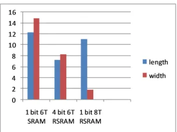
TAB.2: Area comparision 1-bit 6T
SRAM
4-bit 6T RSRAM
1-bit 8T RSRAM
Length (µm)
12.24 28.765 11.06
Width (µm)
14.85 23.845 14.25
Above table shows the area comparisons of 6T SRAM cell, 6T RSRAM cell and 8T RSRAM cell.
Fig. 16:The above graph represents the area comparision of 6T SRAM, 6T RSRAM and 8T RSRAM
V. CONCLUSION
In this paper we proposed a RSRAM cell design without any Area or performance penalty on the SRAM cell.
Proposed RSRAM uses one extra word line and SRAM access transistors are connected to any one of the two word lines depending on the data to be stored in the ROM. Then we embedded this RSRAM circuit in BIST and we tested the RSRAM using test patterns which are produced from BIST circuit. Power of 6T SRAM and 6T R-SRAM are compared by using cadence virtuoso tool.
ACKNOWLEDGMENT
We indebted to our project guide Mr.K.SIVA NAGI REDDY M.E,(Ph.D), Associate Professor of Electronics &
Communication Engineering, Sridevi Women’s Engineering College V.N.Pally, Hyderabad for his excellent guidance, constant inspiration and encouragement in completion of this dissertation.We wish to express gratitude to the project coordinator Dr. B.K.MADHAVI, Professor of Electronics and Communications Engineering Sridevi Women’s Engineering College, V.N.Pally, Hyderabad for supporting us throughout the period of the project.
REFERENCES
[1] Infineon. (2007). 90 nm CMOS Platform Technology, Neubiberg,Ger-many[Online].
Available: http://www.infineo n.com.
[2] D. Lee, S. P. Park, A. Goel, and K. Roy, “Memory-based embedded digital ATE,” in Proc. VLSI Test Symp., May 2011, pp. 266–271.
[3] M. Frigg and S. G. Johnson, “The design and implementation of FFTW3,” Proc. IEEE, vol. 93, no. 2, pp.
216–231, Feb. 2005.
[4] M. Shin and I. Park, “SIMD processor-based turbo decoder supporting multiple third-generation wireless standards,” IEEE Trans. Very Large Scale Integration. (VLSI) Syst., vol. 15, no. 7, pp. 801–810, Jul. 2007.
[5] J. Hennesy and D. Patterson, Computer Architecture: A Quantitative Approach. San Mateo, CA: Morgan Kaufman, 2007.
[6] L. Chang, R. K. Montoye, Y. Nakamura, K. A. Batson, R.
J. Eickemeyer, R.H. Dennard, W. Haensch, and D. James,
“An 8T-SRAM for variability tolerance and low-voltage operation in high-performance caches,” IEEE J. Solid-State Circuits, vol. 43, no. 4, pp. 956–963, Apr. 2008.
[7] S. Nalem and B. H. Calhoun, “Asymmetric sizing in a 45nm 5T SRAM to improve read stability over 6T,” in Proc.Custom.
[8] O.Wood, C.Koay, K Petrillo, H.Mizuno, S.Raghunathan, J.Arnold, D.Horak, M.Burkhardt, G.McIntyre, Y. Deng, B.
La Fontaine, U. Oko-roanyanwu, A. Tchikoulaeva, T.
Wallow, H.-C. James, M. Colburn, S. S. C. Fan, Bala S.
Haran, and Y. Yin, „„Integration of EUV lithography in the fabrication of 22-nm node devices,‟‟ Proc. SPIE vol. 7271, pp. 727104-1–727104-2, 2009
[9]Ashok K. Sharma, “Semiconductor Memories Technology, Testing & Reliability”, IEEE Press, 1997, (©
2005 IEEE, Reprinted with permission)
[10]A. J. van de Goor, “Testing Semiconductor Memories:
Theory and Practice”, John Wiley and Sons, U. S. A, 1995.
[11] S. M. Gold and M. Lamere, “Combining RAM and ROM into a single memory array,” U.S. Patent 6 438 024, Aug. 20, 2002.
[12][Al-Asaad 98]Al-Asaad, H., B.T. Murray, and J.P. Hayes,
“Online BIST for Embedded Systems,” IEEE Design & Test of Computers, pp.17-24, 1998
[13]. V D Agrawal, C R Kime and K K Saluja– “A Tutorial on Built-In Self-Test – Part 1: Principles”, IEEE Design &
Test Of Computers, Volume: 10 Issue: 1, March 1993 Page(s): 73 –82.
[14]. Charles E. Stroud, “A Designer’sGuide to Built-In Self-Test”, Kluwer Academic Publishers, Massachusetts, 2002.
[15]“Generic BIST Block Guide”, Freescale Semiconductor Ltd., Revision 4.5, Dec2003
[16]. Abramovici, Miron – “Digital systems testing and testable design”,Piscataway, NJ: IEEE Press, c1990.
[17]. Bushnell, Michael L – “Essentials of electronic testing for digital, memory, and mixed-signal VLSI circuits”,Boston : Kluwer Academic, c2000.
[18]. Janusz Rajski, Jerzy Tyszer - “Built-In Self-Test for Embedded Systems”, Prentice-Hall,
[19].Ajay Gadhe, Ujwal ShirodeVol. 3, Issue 1, January -February 2013, pp.1073-1078 “Read stability and Write ability analysis of different SRAM cell Structures.”
[20] Dongsoo Lee, Student Member, IEEE, and Kaushik Roy, Fellow, IEEE ”Area Efficient ROM embedded SRAM CACHE IEEE TRANSACTIONS ON VERY LARGE SCALE INTEGRATION (VLSI) SYSTEMS, VOL. 21, NO.
9, SEPTEMBER 2013.
Krishnakumari KALAKOTI was born in hyderabad, India. She pursuing her M.Tech. from Sridevi women’s engineering college during 2013- 2015.
Her research interests in VLSI
Siva nagireddy KALLI was born in Hyderabad, India. He completed his M.E and pursuing his Ph.D He is presently working as associate professor in Sridevi women’s engineering college. His research interests in VLSI and Image processing