ISSN(Online) : 2319-8753 ISSN (Print) : 2347-6710
International Journal of Innovative Research in Science,
Engineering and Technology
(An ISO 3297: 2007 Certified Organization)
Vol. 5, Issue 3, March 2016
An FPGA Implementation of Barrel Shifter
Using Reversible Logic Gates
Mariselvam M #1, Manikandan B#2
Assistant Professor, Department of Electronics and Communication Engineering, JNN Institute of Engineering,
Chennai, India
ABSTRACT: The conservative reversible gates are used to designed reversible sequential circuits. The sequential circuits are flip flops and latches. The conservative logic gates are Feynman, Toffoli, and Fredkin.the design of two vectorstestable sequential circuits based on conservative logic gates.All sequential circuit based onconservative logic gates can be tested for classical unidirectionalstuck-at faults using only two test vectors.The two test vectorsare all 1s, and all 0s. The designs of two vectors testable latches,master-slave flops and double edge triggered (DET) flip-flopsare presented.We also showedthe application of the proposed approach toward 100% faultcoverage for single missing/additional cell defect in the quantum-dot cellular automata (QCA) layout of the Fredkin gate. The conservative logic gates are in terms of complexity, speed and area.
I. INTRODUCTION
Conservative logic is called reversible conservativelogic when there is a one-to-one mapping between the inputsand the outputs vectors along with the property that there areequal number of 1s in the outputs as in the inputs. Conservativelogic circuits are not reversible, if one-to-one mappingbetween the inputs and the outputs vectors is not preserved.
Conservative logic canbe reversible in nature or may not be reversible in nature.Reversibility is the property of circuits in which there is oneto-one mapping between the inputs and the output vectors,that is for each input vector there is a unique output vector andvice-versa.
QCA is one of the emerging nanotechnologies inwhich it is possible to implement reversible logic gates.QCA makes it possible to achieve circuit densities and clockfrequencies beyond the limits of existing CMOS technology. In QCA, computing logic states of 1 and 0 arerepresented by the position of the electrons inside the QCA cell. Thus, when the bit is flippedfrom 1 to 0 there is no actual discharging of the capacitor as inconventional CMOS. Hence, QCA does not have to dissipateall its signal energy during transition. Further, propagationof the polarization from one cell to another is because ofinteraction of the electrons in adjacent QCA cells. As thereis no movement of electrons from one QCA cell to the other,there is no current flow.Therefore, QCA has significant advantagecompared to CMOS technology in terms of power dissipation.Due to high error rates in nano-scale manufacturing, QCA andother nanotechnologies target reducing device error rates.
This paper is organized as follows. Section II presentsthe conservative logic gates,Section III presents design of testablereversible latches, Section IV describes QCA, Section V presents design of testable reversible flip-flop, Section VI discusses theapplication of the proposed two vectors, all 0s and all 1s, Section VII provides somediscussions and conclusions.
II. CONSERVATIVE LOGIC GATES
ISSN(Online) : 2319-8753 ISSN (Print) : 2347-6710
International Journal of Innovative Research in Science,
Engineering and Technology
(An ISO 3297: 2007 Certified Organization)
Vol. 5, Issue 3, March 2016
avoid the fan outproblem in reversible logic. In the Feynman gate, there areexactly two outputs corresponding to the inputs and a ‘0’ inthe second input will copy the first input to both the outputsof that gate. Hence it can be concluded that Feynman gate isthe most suitable gate for single copy of bit since it does not produces any garbage output. The Feynman gate as copying output and NOT functionrespectively. May stuck at 0 or 1 leading to accessingwrong address, no address, or multiple addresses.
Fig.1 Fredkin Gate as AND Gate
Fig.2 New Gate As NAND Gate
Fig.3 New Gate As NOR Gate
Fig.4 Feynman Gate As Copying Output
ISSN(Online) : 2319-8753 ISSN (Print) : 2347-6710
International Journal of Innovative Research in Science,
Engineering and Technology
(An ISO 3297: 2007 Certified Organization)
Vol. 5, Issue 3, March 2016
Novel Reversible Flip Flops are designed using FeynmanGate, New gate and Fredkin Gate. The designed FFs arehighly optimized in terms of number of reversible gates andgarbage outputs.
Reversible logic elements, both with and without the property of conservatism, can be defined in many different logic systems. For the purposes of this paper, the class of reversible elements that can be modeled as binary-valued logic circuits will be called classical reversible logic elements. Much work has been done in defining and characterizing classical reversible logic and applying the concepts toward power conservation and specific technology implementations. This section will briefly define basic results in classical reversible logic.
Table.1 Gate functionality
III. QUANTUM-DOT CELLULAR AUTOMATA
Quantum-dot cellular automata (QCA) is a nanotechnology that has recently been recognized as one of the top six emerging technologies with potential applications in future computers. Several studies have reported that QCA can be used to design general-purpose computational and memory circuits. First proposed in 1993 by Lent et al., and experimentally verified in 1997, QCA is expected to achieve high device density, extremely low power consumption, and very high switching speed. The fundamental QCA logic primitives are the three-input majority gate, wire, and inverter. Each of these can be considered as a separate QCA locally interconnected structure, where QCA digital architectures are combinations of these cellular automata structures. Traditional logic reduction methods, such as Karnaugh maps (K-maps), always produce simplified expressions in the two standard forms: sum of products (SOP) or product of sums (POS). However, we will encounter difficulties in converting these two forms into majority expressions due to the complexity of multilevel majority gates. In CMOS/silicon design, the logic circuits are usually implemented using AND, OR gates based on SOP or POS formats. However, since QCA logic is based on a majority gate primitive, it is critical that an efficient technique be established for designing with this primitive. In this paper, we develop a Boolean algebra based on a geometrical interpretation of three-variable Boolean functions to facilitate the conversion of sum-of-products expressions into reduced majority logic. Thirteen standard functions are introduced, which represent all possible three-variable Boolean functions. For each of these standard functions, we present the reduced majority expression. As an example of this technique, we present a QCA adder design, and show that the proposed method is able to reduce the total hardware, as compared to previously published designs.
A. QCA LOGIC DEVICES
ISSN(Online) : 2319-8753 ISSN (Print) : 2347-6710
International Journal of Innovative Research in Science,
Engineering and Technology
(An ISO 3297: 2007 Certified Organization)
Vol. 5, Issue 3, March 2016
Fig.9 QCA Inverter
B. QCA Clock
A QCA clock consists of four phases which are called Switch, Hold, Release, and Relax as shown in Fig. During the Switch phase, the inter dot barriers are slowly raised and the QCA cells become polarized according to the state of their drivers (that is, their input cells). During the Hold phase, the interdot barriers are kept high and the QCA cells
Fig.10 Four phases of a QCA clock.
ISSN(Online) : 2319-8753 ISSN (Print) : 2347-6710
International Journal of Innovative Research in Science,
Engineering and Technology
(An ISO 3297: 2007 Certified Organization)
Vol. 5, Issue 3, March 2016
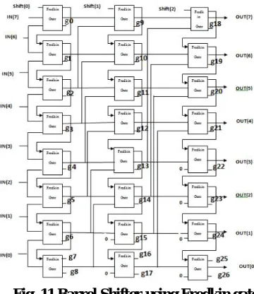
IV. BARREL SHIFTER
Fig. 11 Barrel Shifter using Fredkin gate
A barrel shifter is a combinational logic circuit with n data inputs, n data outputs, and a set of control inputs that specify how to shift the data between input and output. A barrel shifter that is part of a microprocessor CPU can typically specify the direction of shift (left or right), the type of shift (circular, arithmetic, or logical), and the amount of shift (typically 0 to n–1 bits, but sometimes 1 to n bits). In this subsection, well look at the design of a simple 16-bit barrel shifter that does left circular shifts only, using a 4-bit control input S[3:0] to specify the amount of shift. For example, if the input word is ABCDEFGHGIHKLMNOP (where each letter represents one bit), and the control input is 0101 (5), then the output word is FGHGIHKLMNOPABCDE.
The proposed 8-bit barrel shifter is designed using Fredkin gate and reduce the number of gates, low power consumption and quantum cost.
V. TESTING APPROACH TO QCA COMPUTING
QCA computing provides a promising technology to implementreversible logic gates. The QCA design of Fredkin gateusing the four-phase clocking scheme in which the clocking zone is shown by the number next toD (D0 means clock 0 zone, D1 means clock 1 zone, and soon). It can be seen that the Fredkin gate has two level MVimplementation, and it requires 6 MVs and four clocking zonesfor implementation. The number of clocking zones in a QCAcircuit represents the delay of the circuit (delay between theinputs and the outputs). Higher the number of clocking zones,lower the operating speed of the circuit.In QCA manufacturing, defects can occur during the synthesisand deposition phases, although defects are most likely totake place during the deposition phase. Researchers haveshown that QCA cells are more susceptible to missing and additional QCA cell defects. The additional cell defect isbecause of the deposition of an additional cell on the substrate.The missing cell defect is due to the missing of a particularcell. Researchers have been addressing the design and testof QCA circuits assuming the single missing/additional celldefect model.
VI. CONCLUSION
ISSN(Online) : 2319-8753 ISSN (Print) : 2347-6710
International Journal of Innovative Research in Science,
Engineering and Technology
(An ISO 3297: 2007 Certified Organization)
Vol. 5, Issue 3, March 2016
sequential circuitsimplemented using conventional classic gates do not provideinherited support for testability. Hence, a conventionalsequential circuit needs modification in the original circuitryto provide the testing capability. Also as the complexity of a sequential circuit increases the number of test vector requiredto test the sequential circuit also increases. For example, totest a complex sequential circuit thousand of test vectors arerequired to test all stuck-at-faults, while if the same sequentialcircuit is build using proposed reversible sequential buildingblocks it can be tested by only two test vectors, all 0s and all1s. Thus, the main advantage of the proposed conservativereversible sequential circuits compared to the conventionalsequential circuit is the need of only two test vectors to test anysequential circuit irrespective of its complexity. The reductionin number of test vectors minimizes the overhead of test timefor a reversible sequential circuit. The proposed work has thelimitation that it cannot detect multiple stuck-at-faults as wellas multiple missing/additional cell defects. In conclusion, thispaper advances the state-of-the-art by minimizing the numberof test vectors needed to detect stuck-at-faults as well as singlemissing/additional cell defects.
REFERENCES
[1] J. Ren and V. K. Semenov, “Progress with physically and logically reversible superconducting digital circuits,” IEEE Trans. Appl. Super- conduct., vol. 21, no. 3, pp. 780–786, Jun. 2011.
[2] S. F. Murphy, M. Ottavi, M. Frank, and E. DeBenedictis, “On thedesign of reversible QDCA systems,” Sandia National Laboratories,Albuquerque, NM, Tech. Rep. SAND2006-5990, 2006.
[3] H. Thapliyal and N. Ranganathan, “Reversible logic-based concurrentlytestable latches for molecular QCA,” IEEE Trans. Nanotechnol., vol. 9,no. 1, pp. 62–69, Jan. 2010.
[4] P. Tougaw and C. Lent, “Logical devices implemented using quantumcellular automata,” J. Appl. Phys., vol. 75, no. 3, pp. 1818–1825, Nov.1994. [5] P. Tougaw and C. Lent, “Dynamic behavior of quantum cellularautomata,” J. Appl. Phys., vol. 80, no. 8, pp. 4722–4736, Oct. 1996.[6] M. B. Tahoori, J. Huang, M. Momenzadeh, and F. Lombardi, “Testingof quantum cellular automata,” IEEE Trans. Nanotechnol., vol. 3, no. 4,pp. 432–442, Dec. 2004.
[7] G. Swaminathan, J. Aylor, and B. Johnson, “Concurrent testing of VLSIcircuits using conservative logic,” in Proc. Int. Conf. Comput. Design,Cambridge, MA, Sep. 1990, pp. 60–65.
[8] E. Fredkin and T. Toffoli, “Conservative logic,” Int. J. Theor. Phys.,vol. 21, nos. 3–4, pp. 219–253, 1982.
[9] P. Kartschoke, “Implementation issues in conservative logic networks,”M.S. thesis, Dept. Electr. Eng., Univ. Virginia, Charlottesville, 1992.[10] G. Swaminathan, “Concurrent error detection techniques using parity,”M.S. thesis, Dept. Electr. Eng., Univ. Virginia, Charlottesville, 1989. [11] H. Thapliyal, M. B. Srinivas, and M. Zwolinski, “A beginning in thereversible logic synthesis of sequential circuits,” in Proc. Int. Conf.Military Aerosp. Program. Logic Devices, Washington, DC, Sep. 2005,pp. 1–5.
[12] S. Mahammad and K. Veezhinathan, “Constructing online testablecircuits using reversible logic,” IEEE Trans. Instrum. Meas., vol. 59,no. 1, pp. 101–109, Jan. 2010.
[13] H. Thapliyal and N. Ranganathan, “Design of reversible sequentialcircuits optimizing quantum cost, delay and garbage outputs,” ACM J.Emerg. Technol. Comput. Syst., vol. 6, no. 4, pp. 14:1–14:35, Dec. 2010.
[14] M. Hasan, A. Islam, and A. Chowdhury, “Design and analysis of onlinetestability of reversible sequential circuits,” in Proc. Int. Conf. Comput.Inf. Technol., Dec. 2009, pp. 180–185.